EP0320876B1 - Système de traitement pour la collection d'information de fautes - Google Patents
Système de traitement pour la collection d'information de fautes Download PDFInfo
- Publication number
- EP0320876B1 EP0320876B1 EP88120804A EP88120804A EP0320876B1 EP 0320876 B1 EP0320876 B1 EP 0320876B1 EP 88120804 A EP88120804 A EP 88120804A EP 88120804 A EP88120804 A EP 88120804A EP 0320876 B1 EP0320876 B1 EP 0320876B1
- Authority
- EP
- European Patent Office
- Prior art keywords
- control unit
- data
- fault information
- communication
- control
- Prior art date
- Legal status (The legal status is an assumption and is not a legal conclusion. Google has not performed a legal analysis and makes no representation as to the accuracy of the status listed.)
- Expired - Lifetime
Links
Images



Classifications
-
- G—PHYSICS
- G06—COMPUTING OR CALCULATING; COUNTING
- G06F—ELECTRIC DIGITAL DATA PROCESSING
- G06F11/00—Error detection; Error correction; Monitoring
- G06F11/07—Responding to the occurrence of a fault, e.g. fault tolerance
- G06F11/0703—Error or fault processing not based on redundancy, i.e. by taking additional measures to deal with the error or fault not making use of redundancy in operation, in hardware, or in data representation
- G06F11/0766—Error or fault reporting or storing
- G06F11/0772—Means for error signaling, e.g. using interrupts, exception flags, dedicated error registers
-
- G—PHYSICS
- G06—COMPUTING OR CALCULATING; COUNTING
- G06F—ELECTRIC DIGITAL DATA PROCESSING
- G06F11/00—Error detection; Error correction; Monitoring
- G06F11/07—Responding to the occurrence of a fault, e.g. fault tolerance
- G06F11/0703—Error or fault processing not based on redundancy, i.e. by taking additional measures to deal with the error or fault not making use of redundancy in operation, in hardware, or in data representation
- G06F11/0706—Error or fault processing not based on redundancy, i.e. by taking additional measures to deal with the error or fault not making use of redundancy in operation, in hardware, or in data representation the processing taking place on a specific hardware platform or in a specific software environment
- G06F11/0745—Error or fault processing not based on redundancy, i.e. by taking additional measures to deal with the error or fault not making use of redundancy in operation, in hardware, or in data representation the processing taking place on a specific hardware platform or in a specific software environment in an input/output transactions management context
Definitions
- the present invention is directed to a fault information collection processing system in a program-stored communication control processing module for controlling data communication between a central processing unit and data communication lines on the basis of appropriate communication control programs.
- the program of the central processing unit 1 depicted in Fig. 2 involves the preparation of a piece of destination information for the communication as well as a communication statement, and the data are thereby transferred and received by way of input/output channel 3 between communication control processing module 2 and central processing unit 1.
- the particular processing associated with the subsequent data communication is executed on the basis of communication control program 9 in communication control processing module 2.
- Such processing is, as a matter of fact, executed by central control unit 10 which sequentially reads commands from communication control program 9 stored in storage unit 8.
- the prior art communication control processing module is, however, arranged such that the individual component devices are, as illustrated in Fig. 2, radially disposed about central control unit 10 on which the control functions of decrypting and executing communication control program 9 are concentrated.
- central control unit 10 itself has to control the collection of pieces of information on each fault that occurs. It is therefore difficult to collect detailed information.
- channel control unit 7 organizes the fault information gathered by central control unit 10 into information of several bytes.
- the document EP-0 102 434 discloses a processing system provided with a fault detection and fault information gathering arrangement in which a central processing unit is connected to a plurality of communication channels via the system I/O bus, where each communication line connects to the I/O bus through a separate communication channel adapter.
- Each adapter having a fault detection means and a register for storing fault information.
- Said fault information of the plurality of adapters are then transferred to a service unit via the central processing unit via system bus and a dedicated interface, which connects the service unit to the central processing unit.
- the service unit then performs an error analysis/ repair and reports the results thereof to the central processing unit.
- a fault information collection processing system characterized in that: a service control unit 32 for effecting control over the collection processing of fault information serves to gather pieces of fault information and identify the component devices in which faults have occurred in any component device of a communication control processing module 22; the fault information is loaded in a predetermined storage region (an expanded log-out region 43) of a storage unit 8; and thereafter the stored fault information is transferred via channel control unit 7 to a central processing unit 1, thus performing the collection-processing of the fault information.
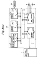
- FIG. 3(A) this is a block diagram of the constitution of a communication control processing module in which a fault information collection processing system representing one embodiment of the present invention is utilized. Components in Fig. 3(A) that correspond to those depicted in Fig. 1 are given the same symbols, and the related description is therefore omitted here.
- the numeral 32 designates a service control unit which is incorporated in a communication control processing module 22 and is adapted to effect control over collection-processing of fault information.
- An appropriate maintenance console generally indicated at 33 is connected to service control unit 32. Note that this console 33 is not necessarily connected to service control unit 32.
- the numeral 34 represents a common data bus through which a storage unit 8, a central control unit 10, a channel control unit 7, a line control unit 11 and service control unit 32 are connected.
- the numeral 35 denotes a signal line via which a group of operation control signals for controlling operational conditions are transmitted from service control unit 32 to storage unit 8, central control unit 10, channel control unit 7 and line control unit 11.
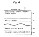
- Fig. 4 is a block diagram illustrating storage regions of storage unit 8 when detailed fault information in communication control processing module 22 is being transferred to central processing unit 1.
- the numeral 41 stands for a communication control program storage region; 42 a buffer region for data transferred and received between data communication lines 4 and 6; 43 an expanded log-out region for temporarily storing detailed fault information; and 44 a transfer program storage region for transferring the data stored in expanded log-out region 43 via channel control unit 7 as well as via input/output channel 3 to central processing unit 1.
- the component device in which the abnormality has been found out serves to inform service control unit 32 of the occurrence of an abnormal condition via signal line 35.
- Service control unit 32 informed of the abnormality in the component device of the communication control processing module through signal line 35, in turn performs control to temporarily freeze the operation of the component device of the communication control processing module through signal line 35, and then collects pieces of detailed fault information specifying the component devices experiencing the faults in question, classifying these faults and indicating their severity through common data bus 34.
- An internal storage region of service control unit 32 temporality stores the detailed fault information which will thereafter be loaded in expanded log-out region 43 of storage unit 8 via common data bus 34.
- the method of identifying the fault information involves the steps of disposing detectors D in predetermined positions of the respective component devices and detecting the fact that signals of given magnitude have been output from given detectors D on the side of service control unit 32.
- Detector D may probably include a temperature detector, voltage detector and current detector, or a program-runaway detector.
- reference to the fault information temporarily stored in service control unit 32 can be made by means of maintenance console 33 connected to service control unit 32.
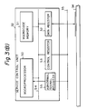
- Fig. 3(B) is a block diagram depicting the internal configuration of the service control unit 32 illustrated in Fig. 3(A).
- reference numeral 50 designates a microprocessor; 51 a microcode memory adapted to store a microcode for controlling microprocessor 50; 52 a data register used for transferring data between microprocessor 50 and common data bus 34; 53 a control register for transferring and receiving signals between signal line 35 and the control register itself in order to control the operation of the communication control processing module as a whole; and 54 a data bus for connecting microprocessor 50, microcode memory 51, data register 52 and control register 53.
- the numeral 55 represents an abnormal signal register for holding abnormal signals from the component devices of the communication control processing module. Abnormal signal register 55 imparts an interruption request to microprocesssor 50 if any abnormal condition occurs in the component device.
- Microprocessor 50 subsequently reads the content of microcode memory 51 and sets the initial data of the intra-device condition information in data register 52 through data bus 54.
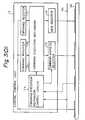
- the control signal transferred to and written into memory data resister 61 of storage unit 8 through common data bus 34 is set in control register 53 via data bus 54.
- Storage unit 8 takes the intra-device condition information present on common data bus 34 into memory data register 61 under control of write/read control circuit 63 upon transmitting the write signal of memory data register 61 via signal line 35.
- Microprocessor 50 further sets the write control signal of storage unit 8 in data register 52 by way of data bus 54, while storage unit 8 writes the content of memory data register 61 into the address specified by memory address register 62 immediately the memory write signal is transmitted via signal line 35.
- Microprocessor 50 advances by one step a value which is to be set in memory address register 62 and reads the next intra-device condition information from microcode memory 51. The operations discussed above are repeated till transfer of all the intra-device condition information has been completed. After transferring all the condition information which has been obtained from the respective component devices incorporated in communication control processing module 22 to expanded log-out region 43 of storage unit 8, microprocessor 50 transmits reset signals for initializing the above-mentioned component devices via data bus 54 to control register 53.
- Microprocessor 50 then sets an initiation address of transfer program storage region 44 of storage unit 8 in data register 52 by way of data bus 54.
- a control signal for transferring to and writing the initiation address into operand register 71 of central control unit 10 via common data bus 34 is set in control register 53 via data bus 54.
- Central control unit 10 operates to take the transfer program initiation address existing on common data bus 34 into operand register 71 under the control of command execution mechanism control circuit 75 upon transmitting the write signal of operand register 71 via signal line 35.
- Microprocessor 50 further sets a control signal for transferring the content of operand register 71 of central control unit 10 to command address register 73 in data register 52 via date bus 54.
- central control unit 10 Upon transmission of the control signal via signal line 35, central control unit 10 transfers the content of operand register 71 to command address register 73 under control of command execution mechanism control circuit 75. Thereafter, microprocessor 50 functions to set an operation resuming signal of central control unit 10 in control register 53 by way of data bus 54. Immediately after the operation resuming signal has been transmitted via signal line 35, central control unit 10 reads a transfer program command from storage unit 8 pursuant to the address assigned to command address register 73, and initiates the execution thereof.
- the description of the transfer program is associated with the commands of central control unit 10.
- Central control unit 10 sequentially reads the commands to command register 70 through common data bus 34 in conformity with the commands, thereby performing the command.
- the intra-device condition information stored in expanded log-out region 43 in accordance with the processing of the transfer program is read into operand register 71 via common data bus 34.
- the intra-device condition information is then set through command execution mechanism 72 in data register 74.
- the intra-device condition information of data register 74 is transferred via common data bus 34 to channel control unit 7, and is then, as in the case of the data transfer of communication control program 9, sent via input/output channel 23 to central processing unit 1.
- a branching command is executed pursuant to the transfer program whereby predetermined initiation address of communication control program storage region 41 is set in command address register 73, thereby reverting to the normal processing of the communication control program.
- the component devices of the communication control processing module include an appropriate service control unit similar to a service processing unit typically added to a sophisticated central processing unit. Whenever a fault occurs in a component device and it is thereby impossible to continue the processing of the communication control program, the service control unit collects pieces of fault information in place of the central control unit and transfers the detailed fault information to the central processing unit.
- This provides the following benefits. It is feasible to gather pieces of fault information pertaining to a plurality of communication control processing modules in the central processing unit. Even in a case where a fault is produced in just one of the plurality of communication control processing modules, the central processing unit is capable of identifying and fixing the faulty device without the burden of needing to gain access to the positions where the respective communication control processing modules are installed.
Landscapes
- Engineering & Computer Science (AREA)
- Theoretical Computer Science (AREA)
- Quality & Reliability (AREA)
- Physics & Mathematics (AREA)
- General Engineering & Computer Science (AREA)
- General Physics & Mathematics (AREA)
- Debugging And Monitoring (AREA)
- Alarm Systems (AREA)
- Maintenance And Management Of Digital Transmission (AREA)
Claims (3)
- Système de traitement pour la collecte d'informations de défauts dans un module (22) de traitement de commande de communication pour commander une communication de données entre un système central de traitement (1), qui exécute des opérations arithmétiques et de commande requises pour le traitement des données, et des lignes (4,6) de communication de données, comprenant :une unité (7) de commande de canaux pour commander des canaux d'entrée et de sortie (3) pour le transfert de données entre ledit système central de traitement (1) et lesdites lignes de communication de données (4,6);une unité de mémoire (8) pour mémoriser un programme de commande de communication et lesdites données devant être transférées;une unité (11) de commande de lignes pour commander le transfert de données en direction et en provenance desdites lignes (4,6) de communication de données; etune unité de commande centrale (10) pour commander les opérations de ladite unité (7) de commande de canaux, de ladite unité de mémoire (8) et de ladite unité (11) de commande de lignes en fonction dudit programme de commande de communication,caractérisé en ce que ladite unité (7) de commande de canaux, ladite unité de mémoire (8), ladite unité (11) de commande de lignes et ladite unité (10) de commande centrale sont connectées à un bus commun (34);ledit système de traitement de commande de communication (22) comprend en outre une unité de commande de service (32) connectée audit bus commun (34); etladite unité de commande de service (32) est adaptée pour contrôler ladite unité (7) de commande de canaux, ladite unité de mémoire (8), ladite unité (11) de commande de lignes et ladite unité de commande centrale (10), collecter une information de défauts provenant de ces unités, et mémoriser temporairement ladite information de défauts dans une région prédéterminée de ladite unité de mémoire (8), et transférer l'information de défauts mémorisés dans ledit système central de traitement (1), pour le traitement ultérieur au moyen de ladite unité (7) de commande de canaux.
- Système de traitement pour la collecte d'informations de défauts selon la revendication 1, dans lequel ladite unité de commande de service (32) comprend :un microprocesseur (50);une mémoire de microcodes (51) adaptée pour mémoriser des microcodes pour la commande dudit microprocesseur (50);un registre de données (52) utilisé pour transférer des données entre ledit microprocesseur (50) et un bus commun de transmission de données (34);un registre de commande (53) pour transférer et recevoir des signaux entre une ligne (35) de transmission de signaux et ledit registre de commande (53) lui-même de manière à commander le fonctionnement dudit module de traitement de commande de communication (22) dans son ensemble;un bus (54) de transmission de données pour connecter ledit microprocesseur (50), ladite mémoire de microcodes (51), ledit registre de données (52) et ledit registre de commande (53); etun registre de signaux anormaux (55) apte à conserver des signaux anormaux provenant de dispositifs formant composants dans ledit module de traitement de commande de communication (22) et créer un signal de demande d'interruption devant être envoyé audit microprocesseur (50) lorsque lesdits signaux anormaux sont reçus.
- Procédé de traitement pour la collecte d'informations de défauts dans un système de traitement de commande de communication à programme mémorisé (22) pour commander des informations de données entre un système central de traitement (1) et des lignes (4,6) de communication de données, ledit procédé étant caractérisé en ce que :(a) tout dispositif, qui est un composant, dans ledit système de traitement de commande de communication (22), dans lequel une anomalie a été trouvée, envoie un signal d'information de défaut à une unité de commande de service (32) située dans ledit système, en étant connecté directement aux dispositifs, qui sont des composants, à l'aide d'un bus commun (34);(b) ladite unité de commande de service (32) commande les opérations normales de tout dispositif, qui est un composant, qui doit être arrêté après la réception dudit signal d'information de défaut;(c) ladite unité de commande de service (32) collecte des signaux détaillés d'informations de défauts, puis transfère les signaux détaillés d'informations de défauts collectés pour le chargement dans une zone de mémoire prédéterminée d'une unité de mémoire (8) dans ledit système;(d) lesdits signaux d'informations de défauts mémorisés sont transmis audit système central de traitement (1) au moyen d'une unité (7) de commande de canaux dans ledit système; et en ce que(e) ledit système central de traitement (1) effectue les opérations de collecte et de traitement desdits signaux détaillés d'informations de défauts.
Applications Claiming Priority (3)
| Application Number | Priority Date | Filing Date | Title |
|---|---|---|---|
| JP31580487 | 1987-12-14 | ||
| JP62315804A JP2519276B2 (ja) | 1987-12-14 | 1987-12-14 | 障害情報収集処理方式 |
| JP315804/87 | 1987-12-14 |
Publications (3)
| Publication Number | Publication Date |
|---|---|
| EP0320876A2 EP0320876A2 (fr) | 1989-06-21 |
| EP0320876A3 EP0320876A3 (fr) | 1990-11-14 |
| EP0320876B1 true EP0320876B1 (fr) | 1999-09-29 |
Family
ID=18069753
Family Applications (1)
| Application Number | Title | Priority Date | Filing Date |
|---|---|---|---|
| EP88120804A Expired - Lifetime EP0320876B1 (fr) | 1987-12-14 | 1988-12-13 | Système de traitement pour la collection d'information de fautes |
Country Status (4)
| Country | Link |
|---|---|
| US (1) | US4985894A (fr) |
| EP (1) | EP0320876B1 (fr) |
| JP (1) | JP2519276B2 (fr) |
| DE (1) | DE3856364T2 (fr) |
Families Citing this family (9)
| Publication number | Priority date | Publication date | Assignee | Title |
|---|---|---|---|---|
| JPH02297228A (ja) * | 1989-05-11 | 1990-12-07 | Fujitsu Ltd | 障害情報格納方式 |
| US5440722A (en) * | 1991-07-22 | 1995-08-08 | Banyan Systems, Inc. | System bus monitor for compiling data regarding use of a system bus |
| JPH0815277B2 (ja) * | 1991-08-09 | 1996-02-14 | インターナショナル・ビジネス・マシーンズ・コーポレイション | パフォーマンス測定値を得るためのシステムおよび方法 |
| US5457781A (en) * | 1993-01-04 | 1995-10-10 | Amdahl Corporation | System having main unit for shutting off clocks to memory upon completion of writing data into memory and information supervising unit to read the data |
| US5642478A (en) * | 1994-12-29 | 1997-06-24 | International Business Machines Corporation | Distributed trace data acquisition system |
| US6470388B1 (en) | 1999-06-10 | 2002-10-22 | Cisco Technology, Inc. | Coordinated extendable system for logging information from distributed applications |
| US7200651B1 (en) | 1999-07-02 | 2007-04-03 | Cisco Technology, Inc. | Dynamic configuration and up-dating of integrated distributed applications |
| US20020104047A1 (en) * | 2001-01-31 | 2002-08-01 | Ncr Corporation | Financial document processing system and method of operating a financial document processing system |
| US20040136708A1 (en) * | 2003-01-15 | 2004-07-15 | Woolf Kevin Reid | Transceiver configured to store failure analysis information |
Family Cites Families (11)
| Publication number | Priority date | Publication date | Assignee | Title |
|---|---|---|---|---|
| US4031375A (en) * | 1973-08-29 | 1977-06-21 | Siemens Aktiengesellschaft | Arrangement for fault diagnosis in the communication controller of a program controlled data switching system |
| US3916178A (en) * | 1973-12-10 | 1975-10-28 | Honeywell Inf Systems | Apparatus and method for two controller diagnostic and verification procedures in a data processing unit |
| US3873819A (en) * | 1973-12-10 | 1975-03-25 | Honeywell Inf Systems | Apparatus and method for fault-condition signal processing |
| JPS5342530A (en) * | 1976-09-29 | 1978-04-18 | Nec Corp | Fault report system |
| US4381540A (en) * | 1978-10-23 | 1983-04-26 | International Business Machines Corporation | Asynchronous channel error mechanism |
| JPS5590160A (en) * | 1978-12-27 | 1980-07-08 | Nec Corp | Transfer system for maintenance information on subordinate controller |
| EP0102434B1 (fr) * | 1982-08-30 | 1986-07-30 | International Business Machines Corporation | Dispositif pour signaler à l'unité de commande centrale d'un équipement de traitement de données, les erreurs se produisant dans les adaptateurs |
| JPS6012849A (ja) * | 1983-07-04 | 1985-01-23 | Hitachi Ltd | 障害情報記録方式 |
| JPS60122407A (ja) * | 1983-12-06 | 1985-06-29 | Fanuc Ltd | プログラマブル・コントロ−ラ |
| JPS61251258A (ja) * | 1985-04-26 | 1986-11-08 | Nec Corp | 通信端末装置 |
| US4713810A (en) * | 1985-09-19 | 1987-12-15 | Gte Sprint Communications Corp. | Diagnostic technique for determining fault locations within a digital transmission system |
-
1987
- 1987-12-14 JP JP62315804A patent/JP2519276B2/ja not_active Expired - Lifetime
-
1988
- 1988-12-13 EP EP88120804A patent/EP0320876B1/fr not_active Expired - Lifetime
- 1988-12-13 DE DE3856364T patent/DE3856364T2/de not_active Expired - Fee Related
- 1988-12-14 US US07/284,078 patent/US4985894A/en not_active Expired - Fee Related
Also Published As
| Publication number | Publication date |
|---|---|
| JPH01156896A (ja) | 1989-06-20 |
| US4985894A (en) | 1991-01-15 |
| JP2519276B2 (ja) | 1996-07-31 |
| DE3856364D1 (de) | 1999-11-04 |
| EP0320876A3 (fr) | 1990-11-14 |
| DE3856364T2 (de) | 2000-05-11 |
| EP0320876A2 (fr) | 1989-06-21 |
Similar Documents
| Publication | Publication Date | Title |
|---|---|---|
| EP0179425B1 (fr) | Sous-système de maintenance pour réseau de calculateurs | |
| US5442777A (en) | Firmware trace data acquisition method | |
| US4985894A (en) | Fault information collection processing system | |
| JPH0465411B2 (fr) | ||
| US6345370B1 (en) | Method for debugging error in a computer system | |
| JP2776679B2 (ja) | 情報処理システム | |
| US6694395B1 (en) | Information processing unit with a plurality of input/output processors | |
| JP3068524B2 (ja) | リモートデバッグシステム | |
| JP3184099B2 (ja) | ライトキャッシュ装置およびライトキャッシュ回路 | |
| JPH0697990A (ja) | 通信ラインモニタ装置 | |
| JPH02146640A (ja) | システム構成監視方式 | |
| JPH08328607A (ja) | プロセスコンピュータの更新方法 | |
| JP2000357130A (ja) | 周辺制御処理装置、障害解析情報保持方式及び障害解析情報保持方法 | |
| JPS6259816B2 (fr) | ||
| JP2936170B2 (ja) | 障害処理方式 | |
| JP2778343B2 (ja) | 監視制御装置 | |
| JPH05233353A (ja) | 障害解析処理方式 | |
| JPH0198086A (ja) | 測定データ収集システムにおける障害対策方式 | |
| JPS61175835A (ja) | 情報処理システム | |
| JPS63276137A (ja) | 遠隔保守診断方式 | |
| JPH03156646A (ja) | 障害情報の出力方式 | |
| JPS6375854A (ja) | 情報処理システムの障害処理方式 | |
| JPS599924B2 (ja) | 入出力インタ−フエ−スの選択誤り検出方式 | |
| JPS59225420A (ja) | デ−タチヤネル装置の障害検出機構 | |
| JPH0426500B2 (fr) |
Legal Events
| Date | Code | Title | Description |
|---|---|---|---|
| PUAI | Public reference made under article 153(3) epc to a published international application that has entered the european phase |
Free format text: ORIGINAL CODE: 0009012 |
|
| AK | Designated contracting states |
Kind code of ref document: A2 Designated state(s): DE FR GB |
|
| PUAL | Search report despatched |
Free format text: ORIGINAL CODE: 0009013 |
|
| AK | Designated contracting states |
Kind code of ref document: A3 Designated state(s): DE FR GB |
|
| RHK1 | Main classification (correction) |
Ipc: G06F 11/34 |
|
| 17P | Request for examination filed |
Effective date: 19901231 |
|
| 17Q | First examination report despatched |
Effective date: 19940228 |
|
| GRAG | Despatch of communication of intention to grant |
Free format text: ORIGINAL CODE: EPIDOS AGRA |
|
| GRAG | Despatch of communication of intention to grant |
Free format text: ORIGINAL CODE: EPIDOS AGRA |
|
| GRAH | Despatch of communication of intention to grant a patent |
Free format text: ORIGINAL CODE: EPIDOS IGRA |
|
| GRAH | Despatch of communication of intention to grant a patent |
Free format text: ORIGINAL CODE: EPIDOS IGRA |
|
| GRAA | (expected) grant |
Free format text: ORIGINAL CODE: 0009210 |
|
| AK | Designated contracting states |
Kind code of ref document: B1 Designated state(s): DE FR GB |
|
| REF | Corresponds to: |
Ref document number: 3856364 Country of ref document: DE Date of ref document: 19991104 |
|
| ET | Fr: translation filed | ||
| PLBE | No opposition filed within time limit |
Free format text: ORIGINAL CODE: 0009261 |
|
| STAA | Information on the status of an ep patent application or granted ep patent |
Free format text: STATUS: NO OPPOSITION FILED WITHIN TIME LIMIT |
|
| 26N | No opposition filed | ||
| PGFP | Annual fee paid to national office [announced via postgrant information from national office to epo] |
Ref country code: DE Payment date: 20001204 Year of fee payment: 13 |
|
| PGFP | Annual fee paid to national office [announced via postgrant information from national office to epo] |
Ref country code: FR Payment date: 20001212 Year of fee payment: 13 |
|
| PGFP | Annual fee paid to national office [announced via postgrant information from national office to epo] |
Ref country code: GB Payment date: 20001213 Year of fee payment: 13 |
|
| PG25 | Lapsed in a contracting state [announced via postgrant information from national office to epo] |
Ref country code: GB Free format text: LAPSE BECAUSE OF NON-PAYMENT OF DUE FEES Effective date: 20011213 |
|
| REG | Reference to a national code |
Ref country code: GB Ref legal event code: IF02 |
|
| PG25 | Lapsed in a contracting state [announced via postgrant information from national office to epo] |
Ref country code: DE Free format text: LAPSE BECAUSE OF NON-PAYMENT OF DUE FEES Effective date: 20020702 |
|
| GBPC | Gb: european patent ceased through non-payment of renewal fee |
Effective date: 20011213 |
|
| PG25 | Lapsed in a contracting state [announced via postgrant information from national office to epo] |
Ref country code: FR Free format text: LAPSE BECAUSE OF NON-PAYMENT OF DUE FEES Effective date: 20020830 |
|
| REG | Reference to a national code |
Ref country code: FR Ref legal event code: ST |