EP0320916A2 - Mémoire morte électriquement effaçable et programmable utilisant des cellules à portes empilées - Google Patents
Mémoire morte électriquement effaçable et programmable utilisant des cellules à portes empilées Download PDFInfo
- Publication number
- EP0320916A2 EP0320916A2 EP88120919A EP88120919A EP0320916A2 EP 0320916 A2 EP0320916 A2 EP 0320916A2 EP 88120919 A EP88120919 A EP 88120919A EP 88120919 A EP88120919 A EP 88120919A EP 0320916 A2 EP0320916 A2 EP 0320916A2
- Authority
- EP
- European Patent Office
- Prior art keywords
- erasable programmable
- memory device
- erasure
- nonvolatile memory
- set forth
- Prior art date
- Legal status (The legal status is an assumption and is not a legal conclusion. Google has not performed a legal analysis and makes no representation as to the accuracy of the status listed.)
- Granted
Links
Images


Classifications
-
- G—PHYSICS
- G11—INFORMATION STORAGE
- G11C—STATIC STORES
- G11C16/00—Erasable programmable read-only memories
- G11C16/02—Erasable programmable read-only memories electrically programmable
- G11C16/04—Erasable programmable read-only memories electrically programmable using variable threshold transistors, e.g. FAMOS
- G11C16/0408—Erasable programmable read-only memories electrically programmable using variable threshold transistors, e.g. FAMOS comprising cells containing floating gate transistors
-
- G—PHYSICS
- G11—INFORMATION STORAGE
- G11C—STATIC STORES
- G11C16/00—Erasable programmable read-only memories
- G11C16/02—Erasable programmable read-only memories electrically programmable
- G11C16/04—Erasable programmable read-only memories electrically programmable using variable threshold transistors, e.g. FAMOS
- G11C16/0408—Erasable programmable read-only memories electrically programmable using variable threshold transistors, e.g. FAMOS comprising cells containing floating gate transistors
- G11C16/0416—Erasable programmable read-only memories electrically programmable using variable threshold transistors, e.g. FAMOS comprising cells containing floating gate transistors comprising cells containing a single floating gate transistor and no select transistor, e.g. UV EPROM
-
- G—PHYSICS
- G11—INFORMATION STORAGE
- G11C—STATIC STORES
- G11C16/00—Erasable programmable read-only memories
- G11C16/02—Erasable programmable read-only memories electrically programmable
- G11C16/06—Auxiliary circuits, e.g. for writing into memory
- G11C16/08—Address circuits; Decoders; Word-line control circuits
-
- G—PHYSICS
- G11—INFORMATION STORAGE
- G11C—STATIC STORES
- G11C16/00—Erasable programmable read-only memories
- G11C16/02—Erasable programmable read-only memories electrically programmable
- G11C16/06—Auxiliary circuits, e.g. for writing into memory
- G11C16/10—Programming or data input circuits
- G11C16/14—Circuits for erasing electrically, e.g. erase voltage switching circuits
-
- H—ELECTRICITY
- H10—SEMICONDUCTOR DEVICES; ELECTRIC SOLID-STATE DEVICES NOT OTHERWISE PROVIDED FOR
- H10D—INORGANIC ELECTRIC SEMICONDUCTOR DEVICES
- H10D30/00—Field-effect transistors [FET]
- H10D30/60—Insulated-gate field-effect transistors [IGFET]
- H10D30/68—Floating-gate IGFETs
Definitions
- the present invention relates generally to an electrically erasable nonvolatile memory, particularly an electrically erasable and programmable read-only-memory (EEPROM) or electrically alterable ROM (EAROM). More specifically, the invention relates to an EEPROM with a stacked-gate cell.
- EEPROM electrically erasable and programmable read-only-memory
- EAROM electrically alterable ROM
- UV-EPROM ultraviolent ray erasable and programmable ROM
- UV-EPROM For such UV-EPROM, needs for one time PROM (OTP) which is fabricated on a plastic package has been growing in view of practical use.
- OTP PROM
- the usual UV-EPROM which is fabricated on a ceramic serdip package with crystal window is expensive because of high cost for material of the package.
- EPROM is programmed only one time similarly to that of ordinary ROM.
- OTP permits only one time of writing and does not permit to erase data in the cells
- an inspection for writing data in each cell cannot be performed after fabricating the device. This encounters serious problem for maintaining satisfactory liability of the products. Namely, in case of ordinary fuse type or junction type PROM, since inspection can be performed by reading out stored data immediately after writing data, it is unnecessary to perform after assembling the package.
- EPROM charge in a floating gate is apt to leak when defective cell exists. This causes retention problem resulting in lose of written data. For this reason, for EPROM, it is essential to perform inspection for finding read/write error so as to remove the product on which the read/write error is found.
- OTP because it is not possible to perform inspection after assembling, removal of the defective is not possible.
- ISSCC Digest page 76 to page 77 proposes EEPROM which has an erase gate to which electron is injected from a floating gate for performing erasure.
- Such architecture requires the additional erase gate.
- technologies for fabricating the erase gate is applied to UV-EPROM which enables the cell size of UV-EPROM to be smaller than the present, EEPROM cannot be comparable in integration.
- a control gate is extended so as to place one end at an equal level to the floating gate in parallel to the floating gate above a channel. Such construction necessary increase bulk thereof so as not to allow desired integration.
- IEDM Digest page 616 to 617 proposes electrical erasure technologies for memory cell having the same structure as UV-EPROM.
- high potential is applied to source region to inject electron in the source region.
- integration becomes equal to UV-EPROM.
- Such technology is advantageous in view of integration but encounters difficult in assurance of erasure of data. Namely, the cells aligned on each word line have source regions connected to each other. Therefore, erasure of the cells on one word line is performed simultaneously by applying equal voltage, e.g. +1.5V, in theory.
- equal voltage e.g. +1.5V
- erasure may cause to set the threshold level at standard threshold level, e.g. +1.0V.
- over-erasure which may cause substantially low threshold level, e.g. -1.5V can occur.
- Such cells having negative threshold level may operates in depression mode. For this reason, practical implementation of this technology is hardly expected.
- IEEE electron Device Letter Vol. EDL-7, No, 8, 1986, page 465 to page 467 discloses erasure technology for memory cells, each having identical structure to UV-EPROM.
- an erasure pulse which varies level between OV to write level for writing data in the floating gate.
- This technology is established based on a discovery of the phenomena in that hall enters into floating gate in response to trailing edge of HIGH level pulse. This technology has poor reliability.
- a substantial level of drain current which is comparable with that required for writing, e.g. several mA for each bit, is required. Therefore, only one to several words can be erased simultaneously. Because of unacceptably low erasure efficiency, this proposal is not adapted for practical implementation.
- Another object of the invention is to provide EEPROM with stacked gate cells.
- EEPROM has architecture similar to or same as UV-EPROM. Erasure operating is performed by applying negative voltage to control gate so as to inject hall into the floating gate.
- an erasable programmable nonvolatile memory device comprises: a plurality of memory cells, each memory cell including: a semiconductor region; a source and drain regions formed in the semiconductor region; a channel region formed between the source and drain regions; a floating gate formed above the the channel region; a first insulating layer disposed between the channel region and the floating gate; a control gate formed above the floating gate; a second insulating layer disposed between the floating gate and the control gate; and means for applying a positive voltage to the control gate for injecting electron in the floating gate for writing and applying a negative voltage to the control gate for injecting hall in the floating gate for erasure.
- the means selective perform erasure operation for each memory cell.
- the means may simultaneously perform erasure operation for each memory cell block composed of a plurality of memory cells.
- the means may comprise a negative voltage source means fabricated in a common package to the memory cells. Also, the means may be connected to the control gate of memory cells via a word line which is connected to a word line decoder via a transferring MOS transistor, the MOS transistor being formed in a well region of the semiconductor region. In such case, the transferring MOS transistor is designed for operation in duplication mode.
- the means applies negative voltage for control gate of selected memory cell and positive voltage for control gate of memory cell which is not selected.
- the control gates of respective memory cells are connected to a word line decoder via a plurality of word lines, and the means sets level of the word lines selected for erasure at LOW level of the word lines which are not selected, at HIGH level, and subsequently applies the negative voltage for selected word lines.
- the control gates of respective memory cells are connected to a word line decoder via a plurality of word lines, and the means latches outputs of the word line decoder, sets levels of all of the word lines at LOW level, and subsequently applies the negative voltage for word lines selected for erasure.
- an erasable programmable nonvolatile memory device comprises: a plurality of memory cells, each including a semiconductor region defining therein a source region, a drain region and a channel region defined between the source and drain regions, a floating gate formed above the the channel region and insulated therefrom, and a control gate formed above the floating gate and insulated therefrom, the memory cell being designed for writing in a bit data by injecting electron in the floating gate; and means for applying a erasure voltage to the control gate for lowering gate junction breakdown voltage at a junction between the semiconductor region and the drain region, and applying a drain voltage for causing breakdown at the junction so as to inject hall in the floating gate for erasure.
- the means transfers the erasure voltage through the word line.
- the memory cells and the means are composed in a single package.
- Fig. 1 shows a cross section of a memory cell forming a part of the preferred embodiment of he erasable programmable nonvolatile memory device.
- the memory cell in the preferred embodiment of the erasable programmable nonvolatile memory device has stacked gate structure. Namely, as seen from Fig. 1, N type source region 2 and N type drain region 3 are formed on a P type semiconductor substrate 1.
- a floating gate 4 is formed above a channel between the source region 2 and the drain region 3 and opposes to the channel via a gate insulation layer 5.
- a control gate 6 is formed above the floating gate 4 in opposition to the latter via a gate insulation layer 7. To the control gate, a control gate voltage V cg is applied.
- a drain volgate V d is applied to the drain region 3.
- the shown structure of the memory cell employed in the preferred embodiment of the erasable programmable nonvolatile memory device according to the present invention is the same as that in UV-EPROM.
- a predetermined voltage e.g.+7 to +12V of drain voltage V d is applied to the drain region 3.
- a predetermined voltage, e.g. +12.5V, of the control gate voltage V cg is applied to the control gate 6.
- an avalanche current is created to flow between the drain region 3, the source region 2 and the semiconductor substrate 1.
- Avalanche current further generates substrate current in the semiconductor substrate 1.
- hot electron is injected into the floating gate 4 via a pinch off region formed in the vicinity of the drain region 3.
- the erasure in the shown embodiment of the erasable programmable nonvolatile memory device according to the present invention is performed by applying a predetermined negative voltage, e.g. -3 to -10V to the control gate 6. Simultaneously, a drain voltage V d equivalent to that applied in writing is applied to the drain region 3. This causes electrical erasure of the written data in the memory cell.
- a predetermined negative voltage e.g. -3 to -10V
- the gate insulating layer 5 formed by oxide layer has high energy barrier property so as not to allow injection of hall to the floating gate.
- the energy level of the hall generated by breakdown is sufficiently high to be injected over the energy barrier of the insulating layer 5.
- the amount of hall and electron in other words, number of carrier, generated upon breakdown at the PN junction, is relatively large. Therefore, erasure can be completed at relatively short period. Practically, the period required for erasure by applying the negative voltage as the control gate voltage V cg is equivalent to the writing in period.
- each memory cell can be selectively erased. This means that the shown embodiment of EEPROM allows to selectively erase each bit.
- the absolute value of the negative control gate voltage V cg required for forming electric field suitable for injecting hall into the floating gate 4 can be reduced in a magnitude of the negative charge in the floating gate.
- EEPROM erasable programmable nonvolatile memory device
- the control gate 6 performs erasure operation by applying the negative voltage for the control gate 6.
- connecting the control gate to the external negative voltage source requires additional terminal to increase number of pins for interfacing. Therefore, it is advantageous to form a negative voltage generator circuit in the memory device.
- the preferred construction of a negative voltage generator circuit employed in the shown embodiment of the EEPROM is shown in Figs. 2(A) and 2(B).
- the negative voltage generator circuit is formed on the semiconductor substrate 1.
- a N type semiconductor region 8 is formed on the P type semiconductor substrate.
- P channel MOS transistors Tr2 and Tr3 are formed. These MOS transistors TR2 and Tr3 are connected in series to each other. One end of the series circuit is connected to the ground. The other end of the series circuit is connected to a word line WL. As is well known, the word line WL is connected to control gates 6 of respective memory cell.
- the word line WL is connected to control gates 6 of respective memory cell.
- the transistors Tr2 and Tr3 and the capacitor C1 form a charge pump circuit for transferring negative voltage through the word line WL.
- the MOS transistor Tr3 is turned ON. By this, a level at the junction between the MOS transistors Tr3 and Tr2 becomes zero or approximately zero including a level shift for V th . Then, at the trailing edge of the HIGH level pulse varying from 5V to OV, the MOS transistor Tr3 is turned OFF and the MOS transistor Tr2 is turned ON. By this source level of the MOS transistor Tr2 is lowered according to lowering of the pulse level and becomes minus. Assuming the level shift V th of the MOS transistors Tr2 and Tr3 is lV, the negative voltage in a level of -3V to -5V can be generated. If greater negative voltage is required, a plurality of charge pump circuits may be formed and connected in series.
- Another N type semiconductor region 9 is formed on the P type semiconductor substrate 1.
- a transferring P channel MOS transistor Tr1 is formed in the N type semiconductor region 9.
- This transferring MOS transistor Tr1 is provided for avoiding direct connection between the word line WL and the semiconductor substrate 1. Namely, the charge level in the word line WL becomes negative in relation to the charge level of the semiconductor substrate 1.
- the negative voltage for erasure operation causes forward bias at the PN junction between the P type semiconductor substrate 1 and the N type semiconductor region 9 to establish direct connection.
- the MOS transistor Tr1 prevent the negative voltage in the word line WL from leaking to the P type semiconductor substrate.
- Fig. 3 In the practical application of the negative voltage generator circuit set forth above, is shown in Fig. 3. As seen from Fig. 3, the negative voltage generator circuit is coupled with a row decoder. The preferred circuit construction according to the present invention is compared with the row decoder circuit employed in the conventionally known UV-EPROM.
- the row decoder circuit includes N channel MOS transistors Tr4, Tr5, Tr6 and Tr7 which receive address signals from a pre-decoder (not shown).
- the row decoder also has a P channel MOS transistor Tr8 serving as a load for the N channel transistors Tr4, Tr5, Tr6 and Tr7.
- These MOS transistors Tr4, Tr5, Tr6, Tr7 and Tr8 form decoding section.
- the row decoder circuit further includes a CMOS inverter constituted by N channel MOS transistor Tr9 and P channel MOS transistors Tr10.
- the CMOS inverter inverts the output signal V N1 of the decoding section.
- the CMOS inverter is connected to the word line WL via a N channel MOS transistor Tr11 and the transferring P channel MOS transistor Tr1 for transferring the output of the CMOS inverter therethrough.
- the N channel MOS transistor Tr11 is designed to be driven by an erasure command Erase .
- the N channel MOS transistor Tr11 is normally maintained ON state and turned into OFF state in response to the erasure command Erase .
- the junction between the MOS transistors Tr11 and Tr1 is connected to the output of the decoding section constituted by the N channel MOS transistors Tr4, Tr5, Tr6 and Tr7 via N channel transistor Tr12.
- the N channel transistor Tr12 is designed to be controlled by the erasure command Erase to be turned ON by the erasure command for inverting the logic of the voltage V N2 .
- CMOS inverter for inverting voltage V WL on the word line WL is formed by P channel MOS transistor TR14 and N channel MOS transistor Tr15.
- the output of this CMOS inverter is applied applied to a gate of P channel MOS transistor Tr13 disposed between V PP /V CC terminal and the word line WL.
- the circuit constituted by the MOS transistors Tr13, Tr14 and Tr15 is designed for selectively applying V PP to the word line WL during programming and V CC during reading out.
- the charge pump circuit including the P channel MOS transistors Tr2 and Tr3 and the capacitor C1 is connected to the ground via a N channel MOS transistor Tr16.
- the N channel MOS transistor Tr16 is controlled by the erasure command Erase .
- the capacitor C1 is also connected to NOR gate NOR1 which receives erasure pulse at one input terminal and the word line voltage V WL of the word line WL.
- V PP /V CC represents V PP /V CC terminal in the row decoding system, for example V PP is +12.5V and V CC is 5V.
- Source is a source of cell array.
- V thp is a threshold voltage of the P channel MOS transistor Tr 1 , -represents a negative voltage, F1 is a floating gate. It should be noted, F1 can be replaced by 5V.
- the row decoder circuit operates as follows.
- the MOS transistor Tr11 is turned OFF and the MOS transistor Tr12 is turned ON, which states of the transistors is alternative to that in the normal state. Therefore, the logic is reversed. Therefore, the voltage V N2 becomes 0V when selected and +5V when not selected. This causes the word line voltage V WL on the word line WL negative.
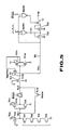
- Fig. 5 shows a modification of the row decoder circuit of Fig. 3, which is also applicable for the preferred embodiment of the erasable programmable nonvolatile memory device according to the invention.
- the shown modification improves the performance of the row decoder circuit of Fig. 3.
- the threshold voltage level V chp of the transferring MOS transistor Tr1 is set at approximately 0V (0 ⁇ 0.2V).
- the threshold voltage V chp of the transferring MOS transistor Tr1 close to 0V, the word line voltage V WL of the non-selected word line WL can be maintained approximately 0V during writing and reading operation. This successfully prevent the leak current from flowing through the blank memory cell.
- the output of the NOR gate NOR2 is applied to the MOS transistor Tr16.
- the NOR gate NOR2 receives the erasure command Erase at one input terminal and the word line voltage V WL at the other input terminal. With this circuit construction, NOR gate is turned OFF by the 5V of the non-selected word line WL. Therefore, the voltage in the charge pump circuit will never affect for the non-selected word line.
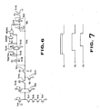
- Fig. 6 shows another modification of the row decoder circuit which also improves the defects in the embodiment of Fig. 3.
- the row decoder of Fig. 6 is designed to latch word lines by recognizing selected word line and non-selected word lines before performing erasure operation.
- the charge in respective word lines WL is initially discharged to set at 0V. Thereafter, the negative voltage for erasure is applied for the selected word lines WL.
- Fig. 7 shows wave form of control signals E1, E2 and E3 used in this modification. The signal levels of these control signals E1, E2 and E3 during writing and reading are maintained at 0V. In this modification, it is not required to reverse logic in the word lines WL between write-read mode operation and erasure mode operation.
- the MOS transistors Tr13, Tr14 and Tr15 basically operates to adjust the word line voltage V WL to V PP during programming operation and to V CC during reading operation.
- these MOS transistors TR13, Tr14 and Tr15 serve for latching signals on the word lines to store information of selected word lines and non-selected word lines. Namely, when the control signal E1 turns into HIGH level, the MOS transistor Tr18 is turned OFF. At this, the signals on respective word lines WL is latched by the MOS transistors Tr13, Tr14 and Tr15. With a certain delay of leading edge of the HIGH level control signal E1, the HIGH level control signal E2 rises. In response to rising of the HIGH level control signal E2, the MOS transistor Tr11 is turned OFF.
- the MOS transistor Tr17 is turned ON to allow the charge in respective word line WL to be discharged.
- the voltage level at respective word line WL is set at 0V.
- the HIGH level control signal E3 rises to turn the transferring MOS transistor, Tr1 OFF.
- the charge pump circuit is selectively operated according to the charge pulse ⁇ generated by the circuit of the MOS transistors Tr13, Tr14 and Tr15 to feed negative voltage for the selected word lines.
- the threshold voltage level V th of the transferring MOS transistor Tr1 is also set at 0 ⁇ 0.2V
- erasure operation is performed by adjusting V CC at approximately 4V for 10 to 100 microseconds. Subsequently blank check is performed. Erasure and blank check operations are repeated for several cycles. When sufficient blank condition cannot be obtained after given cycles of erasure and blank check operation, the V CC level is slightly risen.
- the negative voltage can be controlled by adjusting V CC . Such process is effective for avoiding creation of excessive hall.
- writing operation is performed by writing utilizing 0.1 to 1 miliseconds width write pulse and subsequently perform verification, and repeating writing and verifying for several cycles.
- the shown embodiment of the erasable programmable nonvolatile memory device according to the present invention is enabled to electrically erase the written data. Therefore, even when the EEPROM is fabricated on the plastic package, write test can be performed after assembling. This clearly improves liability of the products. Furthermore, since as illustrated hereabove, since the construction of each memory cell is identical to the UV-EPROM, high integration can be obtained for allowing the memory device to be compact comparable with the UV-EPROM.
Landscapes
- Engineering & Computer Science (AREA)
- Microelectronics & Electronic Packaging (AREA)
- Non-Volatile Memory (AREA)
- Read Only Memory (AREA)
- Semiconductor Memories (AREA)
- Semiconductor Integrated Circuits (AREA)
Applications Claiming Priority (2)
| Application Number | Priority Date | Filing Date | Title |
|---|---|---|---|
| JP62318172A JPH01158777A (ja) | 1987-12-15 | 1987-12-15 | フローティングゲート型不揮発性メモリ |
| JP318172/87 | 1987-12-15 |
Publications (3)
| Publication Number | Publication Date |
|---|---|
| EP0320916A2 true EP0320916A2 (fr) | 1989-06-21 |
| EP0320916A3 EP0320916A3 (fr) | 1991-03-27 |
| EP0320916B1 EP0320916B1 (fr) | 1994-06-29 |
Family
ID=18096272
Family Applications (1)
| Application Number | Title | Priority Date | Filing Date |
|---|---|---|---|
| EP88120919A Expired - Lifetime EP0320916B1 (fr) | 1987-12-15 | 1988-12-14 | Mémoire morte électriquement effaçable et programmable utilisant des cellules à portes empilées |
Country Status (5)
| Country | Link |
|---|---|
| US (1) | US5136541A (fr) |
| EP (1) | EP0320916B1 (fr) |
| JP (1) | JPH01158777A (fr) |
| KR (1) | KR890010918A (fr) |
| DE (1) | DE3850482T2 (fr) |
Cited By (5)
| Publication number | Priority date | Publication date | Assignee | Title |
|---|---|---|---|---|
| US5235544A (en) * | 1990-11-09 | 1993-08-10 | John Caywood | Flash EPROM cell and method for operating same |
| EP0570597A4 (en) * | 1991-12-09 | 1998-11-11 | Fujitsu Ltd | Flash memory improved in erasing characteristic, and circuit therefor |
| US6122199A (en) * | 1996-03-28 | 2000-09-19 | Siemens Aktiengesellschaft | Semiconductor storage device |
| EP0558404A3 (fr) * | 1992-02-24 | 2000-10-11 | Sony Corporation | Mémoire à transistor unique électriquement programmable du type flash |
| WO2002056316A1 (fr) * | 2001-01-12 | 2002-07-18 | Hitachi, Ltd. | Memoire remanente a semi-conducteur |
Families Citing this family (20)
| Publication number | Priority date | Publication date | Assignee | Title |
|---|---|---|---|---|
| DE69024086T2 (de) * | 1989-04-13 | 1996-06-20 | Sundisk Corp | EEprom-System mit Blocklöschung |
| US5265052A (en) * | 1989-07-20 | 1993-11-23 | Texas Instruments Incorporated | Wordline driver circuit for EEPROM memory cell |
| JP3099887B2 (ja) * | 1990-04-12 | 2000-10-16 | 株式会社東芝 | 不揮発性半導体記憶装置 |
| US6002536A (en) * | 1990-07-06 | 1999-12-14 | Hitachi Ltd. | Digital transmission signal processing system and recording/reproducing system |
| US5519654A (en) * | 1990-09-17 | 1996-05-21 | Kabushiki Kaisha Toshiba | Semiconductor memory device with external capacitor to charge pump in an EEPROM circuit |
| US5289423A (en) * | 1990-11-16 | 1994-02-22 | Sgs-Thomson Microelectronics S.R.L. | Bank erasable, flash-EPROM memory |
| JP3068291B2 (ja) * | 1990-12-12 | 2000-07-24 | 新日本製鐵株式会社 | 半導体記憶装置 |
| JP2794974B2 (ja) * | 1991-04-10 | 1998-09-10 | 日本電気株式会社 | 不揮発性半導体記憶装置の起動方法 |
| JP2835215B2 (ja) * | 1991-07-25 | 1998-12-14 | 株式会社東芝 | 不揮発性半導体記憶装置 |
| JPH05102438A (ja) * | 1991-10-04 | 1993-04-23 | Mitsubishi Electric Corp | 不揮発性半導体記憶装置 |
| WO1996008821A1 (fr) * | 1994-09-13 | 1996-03-21 | Macronix International Co., Ltd. | Architecture de circuit integre de memoire flash eprom |
| JP3267436B2 (ja) * | 1993-04-19 | 2002-03-18 | 三菱電機株式会社 | 半導体装置 |
| EP0806045B1 (fr) * | 1995-01-26 | 2001-11-28 | Macronix International Co., Ltd. | Circuit d'attaque en reponse a des adresses decodees de ligne de mots a modes de tensions positive et negative |
| US6021083A (en) * | 1997-12-05 | 2000-02-01 | Macronix International Co., Ltd. | Block decoded wordline driver with positive and negative voltage modes |
| WO1999030326A1 (fr) * | 1997-12-05 | 1999-06-17 | Macronix International Co., Ltd. | Circuit d'attaque de memoire a modes de tension variables |
| KR100418718B1 (ko) * | 2000-06-29 | 2004-02-14 | 주식회사 하이닉스반도체 | 플래쉬 메모리 셀의 소거 방법 |
| CN100334715C (zh) * | 2003-01-14 | 2007-08-29 | 力旺电子股份有限公司 | 非易失性存储元件 |
| JP2006086892A (ja) * | 2004-09-16 | 2006-03-30 | Seiko Instruments Inc | 半導体集積回路装置 |
| KR100843037B1 (ko) * | 2007-03-27 | 2008-07-01 | 주식회사 하이닉스반도체 | 플래시 메모리 장치 및 이의 소거 방법 |
| US8913436B2 (en) * | 2013-03-14 | 2014-12-16 | Freescale Semiconductor, Inc. | Non-volatile memory (NVM) with word line driver/decoder using a charge pump voltage |
Family Cites Families (12)
| Publication number | Priority date | Publication date | Assignee | Title |
|---|---|---|---|---|
| JPS6025837B2 (ja) * | 1978-09-14 | 1985-06-20 | 株式会社東芝 | 半導体記憶装置 |
| JPS5619676A (en) * | 1979-07-26 | 1981-02-24 | Fujitsu Ltd | Semiconductor device |
| US4377857A (en) * | 1980-11-18 | 1983-03-22 | Fairchild Camera & Instrument | Electrically erasable programmable read-only memory |
| GB2094086B (en) * | 1981-03-03 | 1985-08-14 | Tokyo Shibaura Electric Co | Non-volatile semiconductor memory system |
| JPS58182876A (ja) * | 1982-04-21 | 1983-10-25 | Oki Electric Ind Co Ltd | 半導体メモリ素子の製造方法 |
| EP0100772B1 (fr) * | 1982-08-06 | 1987-11-19 | Deutsche ITT Industries GmbH | Matrice de mémoire électrique programmable |
| EP0108681A3 (fr) * | 1982-11-04 | 1986-10-15 | FAIRCHILD CAMERA & INSTRUMENT CORPORATION | Mémoire programmable électriquement effaçable par bit |
| JPS59124095A (ja) * | 1982-12-29 | 1984-07-18 | Fujitsu Ltd | 半導体記憶装置 |
| JPH077599B2 (ja) * | 1984-05-25 | 1995-01-30 | 株式会社日立製作所 | 半導体集積回路装置 |
| JPH0697696B2 (ja) * | 1985-04-23 | 1994-11-30 | 株式会社東芝 | 不揮発性半導体メモリ素子 |
| US4769787A (en) * | 1985-07-26 | 1988-09-06 | Hitachi, Ltd. | Semiconductor memory device |
| JPS63249375A (ja) * | 1987-04-06 | 1988-10-17 | Oki Electric Ind Co Ltd | 半導体記憶装置のデ−タ消去方法 |
-
1987
- 1987-12-15 JP JP62318172A patent/JPH01158777A/ja active Pending
-
1988
- 1988-12-13 US US07/283,795 patent/US5136541A/en not_active Expired - Lifetime
- 1988-12-14 DE DE3850482T patent/DE3850482T2/de not_active Expired - Fee Related
- 1988-12-14 EP EP88120919A patent/EP0320916B1/fr not_active Expired - Lifetime
- 1988-12-15 KR KR1019880016685A patent/KR890010918A/ko not_active Ceased
Cited By (8)
| Publication number | Priority date | Publication date | Assignee | Title |
|---|---|---|---|---|
| US5235544A (en) * | 1990-11-09 | 1993-08-10 | John Caywood | Flash EPROM cell and method for operating same |
| EP0570597A4 (en) * | 1991-12-09 | 1998-11-11 | Fujitsu Ltd | Flash memory improved in erasing characteristic, and circuit therefor |
| EP0961289A3 (fr) * | 1991-12-09 | 2000-02-02 | Fujitsu Limited | Mémoire-Flash avec effacement amélioré et circuit associé |
| EP1168362A3 (fr) * | 1991-12-09 | 2004-09-29 | Fujitsu Limited | Mémoire Flash permettant un meilleur effacement |
| EP1168365A3 (fr) * | 1991-12-09 | 2004-09-29 | Fujitsu Limited | Circuit de génération de tension de polarisation négative |
| EP0558404A3 (fr) * | 1992-02-24 | 2000-10-11 | Sony Corporation | Mémoire à transistor unique électriquement programmable du type flash |
| US6122199A (en) * | 1996-03-28 | 2000-09-19 | Siemens Aktiengesellschaft | Semiconductor storage device |
| WO2002056316A1 (fr) * | 2001-01-12 | 2002-07-18 | Hitachi, Ltd. | Memoire remanente a semi-conducteur |
Also Published As
| Publication number | Publication date |
|---|---|
| US5136541A (en) | 1992-08-04 |
| KR890010918A (ko) | 1989-08-11 |
| EP0320916A3 (fr) | 1991-03-27 |
| JPH01158777A (ja) | 1989-06-21 |
| EP0320916B1 (fr) | 1994-06-29 |
| DE3850482T2 (de) | 1995-02-16 |
| DE3850482D1 (de) | 1994-08-04 |
Similar Documents
| Publication | Publication Date | Title |
|---|---|---|
| EP0320916A2 (fr) | Mémoire morte électriquement effaçable et programmable utilisant des cellules à portes empilées | |
| US5347490A (en) | Nonvolatile semiconductor memory device | |
| KR0172441B1 (ko) | 불휘발성 반도체 메모리의 프로그램 방법 | |
| US5841721A (en) | Multi-block erase and verification circuit in a nonvolatile semiconductor memory device and a method thereof | |
| EP0608075B1 (fr) | Mémoires non-volatiles à semi-conducteur | |
| US5299162A (en) | Nonvolatile semiconductor memory device and an optimizing programming method thereof | |
| US4858194A (en) | Nonvolatile semiconductor memory device using source of a single supply voltage | |
| US6288944B1 (en) | NAND type nonvolatile memory with improved erase-verify operations | |
| KR100366741B1 (ko) | 불휘발성 반도체 기억 장치 | |
| EP0558404A2 (fr) | Mémoire à transistor unique électriquement programmable du type flash | |
| US20010017789A1 (en) | Nonvolatile semiconductor memory device having a data reprogram mode | |
| US6466478B1 (en) | Non-volatile semiconductor memory device | |
| KR940006611B1 (ko) | 전기적으로 소거 및 프로그램이 가능한 반도체 메모리장치의 자동 소거 최적화회로 및 방법 | |
| CN1229809C (zh) | 具有读取模式用的字线驱动器的闪存装置及其操作方法 | |
| US20080106949A1 (en) | Array source line (avss) controlled high voltage regulation for programming flash or ee array | |
| US4630087A (en) | Nonvolatile semiconductor memory device | |
| US5481494A (en) | Method for tightening VT distribution of 5 volt-only flash EEPROMS | |
| JP3190031B2 (ja) | 不揮発性半導体記憶装置 | |
| US5684747A (en) | Method for erasing nonvolatile semiconductor memory device incorporating redundancy memory cells | |
| US5253200A (en) | Electrically erasable and programmable read only memory using stacked-gate cell | |
| US5903497A (en) | Integrated program verify page buffer | |
| US5943268A (en) | Non-volatile latch having PMOS floating gate memory cells | |
| JPH07120716B2 (ja) | 半導体記憶装置 | |
| EP0530376B1 (fr) | Memoire a semi-conducteur dotee d'une cellule de memoire remanente a semi-conducteur | |
| JP2732070B2 (ja) | 不揮発性半導体記憶装置の書込み方法 |
Legal Events
| Date | Code | Title | Description |
|---|---|---|---|
| PUAI | Public reference made under article 153(3) epc to a published international application that has entered the european phase |
Free format text: ORIGINAL CODE: 0009012 |
|
| 17P | Request for examination filed |
Effective date: 19890113 |
|
| AK | Designated contracting states |
Kind code of ref document: A2 Designated state(s): DE FR GB NL |
|
| PUAL | Search report despatched |
Free format text: ORIGINAL CODE: 0009013 |
|
| AK | Designated contracting states |
Kind code of ref document: A3 Designated state(s): DE FR GB NL |
|
| 17Q | First examination report despatched |
Effective date: 19930305 |
|
| GRAA | (expected) grant |
Free format text: ORIGINAL CODE: 0009210 |
|
| AK | Designated contracting states |
Kind code of ref document: B1 Designated state(s): DE FR GB NL |
|
| REF | Corresponds to: |
Ref document number: 3850482 Country of ref document: DE Date of ref document: 19940804 |
|
| ET | Fr: translation filed | ||
| PGFP | Annual fee paid to national office [announced via postgrant information from national office to epo] |
Ref country code: GB Payment date: 19941206 Year of fee payment: 7 |
|
| PGFP | Annual fee paid to national office [announced via postgrant information from national office to epo] |
Ref country code: DE Payment date: 19941208 Year of fee payment: 7 |
|
| PGFP | Annual fee paid to national office [announced via postgrant information from national office to epo] |
Ref country code: FR Payment date: 19941209 Year of fee payment: 7 |
|
| PGFP | Annual fee paid to national office [announced via postgrant information from national office to epo] |
Ref country code: NL Payment date: 19941231 Year of fee payment: 7 |
|
| PLBE | No opposition filed within time limit |
Free format text: ORIGINAL CODE: 0009261 |
|
| STAA | Information on the status of an ep patent application or granted ep patent |
Free format text: STATUS: NO OPPOSITION FILED WITHIN TIME LIMIT |
|
| 26N | No opposition filed | ||
| PG25 | Lapsed in a contracting state [announced via postgrant information from national office to epo] |
Ref country code: GB Effective date: 19951214 |
|
| PG25 | Lapsed in a contracting state [announced via postgrant information from national office to epo] |
Ref country code: NL Effective date: 19960701 |
|
| GBPC | Gb: european patent ceased through non-payment of renewal fee |
Effective date: 19951214 |
|
| PG25 | Lapsed in a contracting state [announced via postgrant information from national office to epo] |
Ref country code: FR Effective date: 19960830 |
|
| NLV4 | Nl: lapsed or anulled due to non-payment of the annual fee |
Effective date: 19960701 |
|
| PG25 | Lapsed in a contracting state [announced via postgrant information from national office to epo] |
Ref country code: DE Effective date: 19960903 |
|
| REG | Reference to a national code |
Ref country code: FR Ref legal event code: ST |