EP0323249A2 - Halbleiterkristallstruktur und deren Herstellungsverfahren - Google Patents
Halbleiterkristallstruktur und deren Herstellungsverfahren Download PDFInfo
- Publication number
- EP0323249A2 EP0323249A2 EP88312391A EP88312391A EP0323249A2 EP 0323249 A2 EP0323249 A2 EP 0323249A2 EP 88312391 A EP88312391 A EP 88312391A EP 88312391 A EP88312391 A EP 88312391A EP 0323249 A2 EP0323249 A2 EP 0323249A2
- Authority
- EP
- European Patent Office
- Prior art keywords
- layer
- semiconductor
- atom mono
- layers
- semiconductor layer
- Prior art date
- Legal status (The legal status is an assumption and is not a legal conclusion. Google has not performed a legal analysis and makes no representation as to the accuracy of the status listed.)
- Granted
Links
Images


Classifications
-
- H—ELECTRICITY
- H10—SEMICONDUCTOR DEVICES; ELECTRIC SOLID-STATE DEVICES NOT OTHERWISE PROVIDED FOR
- H10P—GENERIC PROCESSES OR APPARATUS FOR THE MANUFACTURE OR TREATMENT OF DEVICES COVERED BY CLASS H10
- H10P14/00—Formation of materials, e.g. in the shape of layers or pillars
- H10P14/20—Formation of materials, e.g. in the shape of layers or pillars of semiconductor materials
- H10P14/29—Formation of materials, e.g. in the shape of layers or pillars of semiconductor materials characterised by the substrates
- H10P14/2901—Materials
- H10P14/2902—Materials being Group IVA materials
- H10P14/2905—Silicon, silicon germanium or germanium
-
- H—ELECTRICITY
- H10—SEMICONDUCTOR DEVICES; ELECTRIC SOLID-STATE DEVICES NOT OTHERWISE PROVIDED FOR
- H10D—INORGANIC ELECTRIC SEMICONDUCTOR DEVICES
- H10D62/00—Semiconductor bodies, or regions thereof, of devices having potential barriers
- H10D62/40—Crystalline structures
- H10D62/405—Orientations of crystalline planes
-
- H—ELECTRICITY
- H10—SEMICONDUCTOR DEVICES; ELECTRIC SOLID-STATE DEVICES NOT OTHERWISE PROVIDED FOR
- H10P—GENERIC PROCESSES OR APPARATUS FOR THE MANUFACTURE OR TREATMENT OF DEVICES COVERED BY CLASS H10
- H10P14/00—Formation of materials, e.g. in the shape of layers or pillars
- H10P14/20—Formation of materials, e.g. in the shape of layers or pillars of semiconductor materials
- H10P14/29—Formation of materials, e.g. in the shape of layers or pillars of semiconductor materials characterised by the substrates
- H10P14/2901—Materials
- H10P14/2907—Materials being Group IIIA-VA materials
- H10P14/2911—Arsenides
-
- H—ELECTRICITY
- H10—SEMICONDUCTOR DEVICES; ELECTRIC SOLID-STATE DEVICES NOT OTHERWISE PROVIDED FOR
- H10P—GENERIC PROCESSES OR APPARATUS FOR THE MANUFACTURE OR TREATMENT OF DEVICES COVERED BY CLASS H10
- H10P14/00—Formation of materials, e.g. in the shape of layers or pillars
- H10P14/20—Formation of materials, e.g. in the shape of layers or pillars of semiconductor materials
- H10P14/29—Formation of materials, e.g. in the shape of layers or pillars of semiconductor materials characterised by the substrates
- H10P14/2926—Crystal orientations
-
- H—ELECTRICITY
- H10—SEMICONDUCTOR DEVICES; ELECTRIC SOLID-STATE DEVICES NOT OTHERWISE PROVIDED FOR
- H10P—GENERIC PROCESSES OR APPARATUS FOR THE MANUFACTURE OR TREATMENT OF DEVICES COVERED BY CLASS H10
- H10P14/00—Formation of materials, e.g. in the shape of layers or pillars
- H10P14/20—Formation of materials, e.g. in the shape of layers or pillars of semiconductor materials
- H10P14/32—Formation of materials, e.g. in the shape of layers or pillars of semiconductor materials characterised by intermediate layers between substrates and deposited layers
- H10P14/3202—Materials thereof
- H10P14/3214—Materials thereof being Group IIIA-VA semiconductors
- H10P14/3221—Arsenides
-
- H—ELECTRICITY
- H10—SEMICONDUCTOR DEVICES; ELECTRIC SOLID-STATE DEVICES NOT OTHERWISE PROVIDED FOR
- H10P—GENERIC PROCESSES OR APPARATUS FOR THE MANUFACTURE OR TREATMENT OF DEVICES COVERED BY CLASS H10
- H10P14/00—Formation of materials, e.g. in the shape of layers or pillars
- H10P14/20—Formation of materials, e.g. in the shape of layers or pillars of semiconductor materials
- H10P14/34—Deposited materials, e.g. layers
- H10P14/3402—Deposited materials, e.g. layers characterised by the chemical composition
- H10P14/3414—Deposited materials, e.g. layers characterised by the chemical composition being group IIIA-VIA materials
- H10P14/3421—Arsenides
Definitions
- the present invention relates to a novel structure of semiconductor crystals. More particularly, it relates to an improved structure of III-V compound semiconductors having controlled piezoelectric property.
- the semiconductor structure according to the present invention is useful for fabricating elements such as MESFET,HBT, laser diodes or the like.
- the present invention relates also to a process for producing such a novel structure of semiconductor crystals.
- III-V compound semiconductors having a zincblende type crystalline structure such as gallium arsenide (GaAs), indium phosphite (InP) or the like are used as a material for high-speed switching devices or high-frequency amplifying devices owing to their high electron mobility and as a material for light-emitting devices owing to their direct transition type band structure.
- GaAs gallium arsenide
- InP indium phosphite
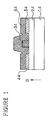
- Fig. 1 illustrates an example of a well-known Schottky barrier type field-effect transistor fabricated on a GaAs substrate.
- an active channel layer 24 is formed by ion implantation technique or the like on a semi-insulating GaAs (100) substrate 14 which is sliced out of an ingot which is prepared by the Czochralski technique.
- a gate electrode 34, a source electrode 44 and a drain electrode 54 are formed and then a protective coating layer 64 made of insulator such as SiO2 is deposited thereon.
- GaAsMESFET Technological trend in GaAsMESFET is to reduce the gate length so as to improve its performance. However, as the gate length is reduced, a so called short-channel effect appears so that leakage of electrons out of a channel region increases and the device characteristics of a short channel FET deviates from a device whose gate length is long. If a FET having such short-channel effect is built in an integrated circuit, the variation in the electrical characteristics become uncontrollable with respect to the variation in gate length but the device parameters are influenced directly by manufacturing conditions such as gate processing, so that it becomes difficult to design the circuits.
- Basic logic elements used in the GaAs integrated circuit built on a GaAs substrate are DCFL (Direct Coupled FET Logic), BFL (Buffered FET Logic), SCFL (Source Coupled FET Logic) or the like.
- DCFL and SCFL are fabricated by different FETs each having its own threshold voltage on a common substrate.
- Japanese patent laid-open No. 60-176,276 utilizes the above-mentioned anisotropy or the piezoelectric charge in the fabrication of an integrated circuit. Namely, in this patent, two FETs having two different threshold voltages are built on a common substrate by changing the orientation of gate electrodes for respective channels each possessing an identical concentration and an identical thickness without increasing the channel forming steps.
- the value of the piezoelectric charge which results in the difference between two threshold voltages is determined by a piezoelectric constant which is inherent in material of the substrate used if the magnitude of the stress applied to the substrate is constant, so that it is impossible to obtain controllably a desired value of the threshold voltage.
- a main object of the present invention is to provide a novel semiconductor having a modified crystalline structure whose symmetrical property can be controlled arbitrarily.
- a specific object of the present invention is to solve the fluctuation in quality of elements fabricated or lack of uniformity in the electric characteristics due to the piezoelectric effect and to provide a structure of semiconductor crystal which permits to realize semiconductor devices whose device properties are not influenced by the stresses.
- Another specific object of the present invention is to provide a structure of semiconductor crystal which can induce a desired value of piezoelectric charge for a given constant thickness of the protective overlay by controlling the piezoelectric constant of the crystal itself.
- Still another specific object of the present invention is to provide a structure of semiconductor crystal which permits to fabricate different FETs each having a desired threshold voltage for a common channel parameter possessing an identical concentration and an identical thickness by controlling the piezoelectric constant of the crystal itself.
- the present invention provides a semiconductor crystal of compound semiconductor material composed of a first element and a second element, characterized in that a plurality of unit layers are stratified periodically on a substrate, each unit layer comprising at least one first semiconductor layer comprising a first atom mono layer of the first element and a second atom mono layer of the second element, the first and second atom mono layers being stratified one over another alternately in a first deposition order, and at least one second semiconductor layer comprising said first atom mono layer and the second atom mono layer which are stratified one over another alternately in the reverse deposition order with respect to the first deposition order of the first semiconductor layer.
- the semiconductor crystal according to the present invention is preferably grown or deposited on a substrate such as a semi-insulating GaAs substrate.
- the semionuctor material of which the semiconductor crystal according to the present invention is composed is compound semiconductor.
- the compound semiconductor material is preferably composed of an element of III group and an element of V group, such as GaAs, InP, InAs, GaP, InGaAs or the like.
- each of the first semiconductor layer and the second semiconductor layer can be a GaAs layer, an InP layer, an InAs layer, a GaP layer, an InGaAs layer or the like.
- the present invention is advantageously applicable to those semiconductor crystals having a zincblende type crystalline structure.
- a semiconductor of GaAs is grown on a semi-insulating GaAs substrate.
- elements of III group such as In and Ga are deposited at a predetermined ratio of fluxes in place of a single flux of Ga.
- a ratio of the total number of the first and second atom mono layers in the first semiconductor layer to the total number of the first and second atom mono layers in the second semiconductor layer can be changed continuously and selected according to the purpose or use.
- the total number of said first and second atom mono layers in the first semiconductor layer is equal to the total number of the first and second atom mono layers in the second semiconductor layer.
- the crystalline structure according to the present invention has such an advantage that the anisotropy caused by the polarization can be eliminated, so that, for example, the dependency of threshold voltage on the gate orientation caused by the piezoelectric effect due to the stress in GaAsMESFET can be eliminated and hence the freedom in design of integrated circuits is increased, and fluctuations of characteristics can be reduced so that uniformity in FET electrical characteristics is improved.
- the total number of the first and second atom mono layers in the first semiconductor layer is not equal to the total number of the first and second atom mono layers in the second semiconductor layer.
- the crystalline structure according to the present invention has such an advantage that the anisotropy caused by the polarization can be controlled intentionally, so that, for example, the short-channel effect can be controlled freely by means of the piezoelectric charges caused by the stress in GaAsMESFET in order to improve the performance and to increase the freedom in design of FET.
- the crystalline structure of this case advantageously permits to control the anisotropic effect caused by polarization continuously.
- the freedom of design in GaAsMESFET which utilizes the piezoelectric effect caused by the stress is advantageously increased so that two different threshold voltages each which depend on the difference in the orientation of respective gates can be realized freely.
- the unit layers are grown or stratified periodically along a direction of [111] axis or [100] axis on the substrate.
- an intermediate layer is interposed between the first semiconductor layer and the second semiconductor layer in order to facilitate growing an upper semiconductor layer.
- Each intermediate layer consists preferably of a plurality of atom mono layers.
- an intermediate layer of Ge is interposed between the first and second GaAs layers, because it is difficult to grow the second GaAs layer directly on the first GaAs layer.
- silicon Si
- Si silicon
- the total number of thickness of the intermediate atom mono layers stratified in the intermediate Ge layer is not necessary to be large. It is also possible to use another element in IV group other than Ge since it is not necessary to take the continuity in the lattice into consideration when the number of atom mono layers used in the Ge layer is small.
- the total number of the atom mono layers stratified in the Ge layer is preferably an even number in order to realize higher effect. Namely, when the number of the atom mono layers stratified in the Ge layer is an odd number, a repetitive order of Ga and As and hence the polarity become identical both in the first GaAs layer and in the second GaAs layer, so that such system can be considered that several atom mono layers in the first GaAs layer are merely replaced by Ge atom mono layers. To the contrary, when the number of the atom mon layers stratified in the Ge layer is an even number, a repetitive order of Ga and As becomes reversed in the first GaAs layer and the second GaAs layer.
- elements of III group such as In and Ga are deposited at a predetermined ratio of fluxes in place of a single flux of Ga.
- a layer of IV group element which has the same function as the intermediate Ge layer can be deposited.
- the structure of the above mentioned semiconductor crystal according to the present invention can be produced by molecular beam epitaxy (MBE) technique which itself is well-known and widely used in the field of IC industry or the like.
- MBE molecular beam epitaxy
- the anisotropy caused by the polarization is eliminated.
- the dependency of threshold voltage on the gate orientation is released from the piezoelectric effect due to the stress in GaAs MESFET, so that the design flexibility of integrated circuits is increased and the fluctuation of electric characteristics is reduced.
- the principle on which the first embodiment of the present invention is based is that the polarity in GaAs is offset in each unit layer because polarization in the first semiconductor layer is directed to [111] while polarization in the second semiconductor layer is directed to [ 1 1 1 ]. Therefore, the piezoelectric polarization due to polarity is offset or cancelled, so that the crystal obtained, as a whole, can be considered macroscopically to be a nonpolar crystal.
- a semiconductor crystal according to the first embodiment has a structure in which each unit layer comprises a first semiconductor layer deposited on a substrate and consisting of at least one layer comprising alternately stratified III group atom mono layer and V group atom mono layer, the III group atom and the V group atom being components of a III-V compound semiconductor having a zincblende type crystal, and a second semiconductor layer deposited on the first semiconductor layer and consisting of at least one layer comprising alternately stratified III group atom mono layer and V group atom mono layer, the order of stratification of the III group atom mono layer and the V group atom mono layer in the second semiconductor layer being reversed with respect to that of the first semiconductor layer, in that more than one of the unit layer is stratified periodically, and in that the number or a thickness of the atom mono layers in the first semiconductor layer is equal to the number or thickness of the atom mono layers in the second semiconductor layer.
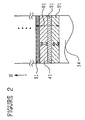
- Fig. 2 is an illustrative cross sectional view showing a crystalline structure of a GaAs MESFET substrate according to the first embodiment of the present invention.
- the crystalline structure shown in Fig. 2 can be prepared, for example, by the following growing technique:
- a semi-insulating (100) GaAs substrate is held on a holder and is heated at a substrate temperature of 650°C in an ultrahigh-vacuum chamber. At first, only one atom mono layer of Ga is deposited on a surface of the semi-insulating (100) GaAs substrate. After a shutter for Ga effusion is closed to arrest a flux of Ga, only one atom mono layer of As is deposited on the Ga atom mono layer.
- the atomic layer epitaxy (ALE) can be realized by repeating such operations so that the growth is effected one atom mono layer at a time. In the case shown in Fig.
- each unit semiconductor layer 61 has a thickness of 67.8 ⁇ and consists of a first GaAs layer 21 consisting of twenty (20) atom mono layers which are formed by the ALE technique and are deposited alternately in the order of Ga-As, a first Ge layer 31 whose thickness corresponds to four (4) atom mono layers of Ge and which is grown by irradiating the flux of Ge continuously, a second GaAs layer 41 consisting of twenty (20) atom mono layers which are grown by the same manner as the first layer 21 except that the order of deposition is As-Ga, and a second Ge layer 51 whose thickness corresponds to four (4) atom mono layers of Ge, and seventy (70) unit semiconductor layers 61 are stratified to have a thickness of 0.47 ⁇ m finally.
- the polarization is cancelled since the direction of polarization in the first GaAs is [111] while the direction of polarization in the second GaAs layer is [ 1 1 1 ].
- the first Ge layer 31 and the second Ge layer 51 are arranged because it is difficult to grow and the second GaAs layer 41 directly on the first GaAs layer 21. Therefore, the number of atom mono layers stratified in the Ge layer is not necessary to be large. It is also possible to use another element in IV group other than Ge since it is not necessary to take the continuity in the lattice into consideration when the number of atom mono layers stratified in the Ge layer is small.
- the number of the atom mono layers stratified in the Ge layer is preferably an even number in order to obtain an improved effect.
- elements of III group such as In and Ga are deposited at a predetermined ratio of fluxes in place of a single flux of Ga.
- a layer of IV group element which has the same function as the Ge layer can be deposited.
- a layer of IV group element which has the same function as the Ge layer can be deposited.
- Fig. 3 shows a cross sectional view of an embodiment of a GaAs MESFET having the crystalline structure of Fig. 2.
- the above-mention crystalline structure 22 according to the present invention is deposited on a GaAs (100) substrate 12. Impurity is doped in a surface of the crystalline structure 22 to produce an active layer 32 having a thickness of 0.1 ⁇ m and a concentration of 2 x 1017 cm ⁇ 3.
- a gate electrode 42, a source electrode 52 and a drain electrode 62 are formed on the active layer 32.
- a surface of the MESFET is covered with a protective overlay 72 composed of SiO2 having a thickness of 1 ⁇ m.
- Example 2 no anisotropy was observed in the case of Example 2 and no deviation from a designed value. This means that the influence caused by the stress is removed.
- Fig. 4 is an illustrative cross sectional view showing a crystalline structure for a GaAs MESFET substrate which is similar to Fig. 2 but shows another example of the first embodiment of the present invention.
- the crystalline structure shown in Fig. 4 is prepared, for example, by the following growing technique:
- a semi-insulating (100) GaAs substrate is held on a holder and is heated at a substrate temperature of 650°C in an ultrahigh-vacuum chamber. At first, only one atom mono layer of Ga is deposited on a surface of the semi-insulating (100) GaAs substrate. After a shutter for Ga effusion is closed to arrest a flux of Ga, only one atom mono layer of As is deposited on the Ga atom mono layer.
- the atomic layer epitaxy (ALE) can be realized by repeating such operations so that the growth is effected one atom mono layer at a time. In the case shown in Fig.
- each unit semiconductor layer 63 has a thickness of 96.1 ⁇ and consists of a first GaAs layer 23 consisting of thirty (30) atom mono layers which are formed by the ALE technique and are deposited alternately in the order of As-Ga, a first Ge layer 33 whose thickness corresponds to four (4) atom mono layers of Ge and which is grown by irradiating the flux of Ge continuously, a second GaAs layer 43 consisting of thirty (30) atom mono layers which are grown by the same manner as the first layer 23 except that the order of deposition is Ga-As, and a second Ge layer 53 whose thickness corresponds to four (4) atom mono layers of Ge, and seventy (70) unit semiconductor layers 63 are stratified to a thickness of 0.67 ⁇ m. In every unit semiconductor layer, the polarization is cancelled since the direction of polarization in the first GaAs is [ 1 1 1 ] while the direction of polarization in the second GaAs layer is [111].
- the Ga layer, the As layer and the Ge layer can be stratified on the other substrate such as Ge (100) substrate, GaAs (111) substrate, Ge(111) substrate or the like in place of the GaAs (100) substrate.
- a superlattice structure of equal polarity can be realized in any polar crystal such as InP whose lattice constant is nearly the same and on which epitaxial growth can be effected, so that homogeneous devices which are free from anisotropy due to the polarity can be manufactured.
- Such superlattice structure having equal polarity can be realized when the crystalline structure according to the present invention is grown along the direction of [111] axis on the substrate.
- the crystalline structure according to the present invention is applicable to any device of compound semiconductors such as hetero bipolar transistors (HBT), laser diodes or the like in addition to the GaAs MESFET shown in the embodiment.
- HBT hetero bipolar transistors
- the first embodiment has a wide applications because the structure can suppress the deviation or shift caused by the stress.
- the crystalline structure according to the first embodiment has such an advantage that the anisotropy caused by the polarization can be eliminated, so that, for example, the dependency of threshold voltage on the gate orientation caused by piezoelectric effect due to the stress in GaAs MESFET can be eliminated and hence the freedom in design of integrated circuits is increased and the fluctuation of characteristics can be reduced, so that uniformity in FET electrical characteristics is improved.
- the anisotropy caused by the polarization is controlled intentionally in order to control, for example, the short-channel effect by means of the piezoelectric charges caused by the stress in GaAsMESFET.
- the principle on which the second embodiment of the present invention is based is such a fact that the polarity in the unit layer is offset when the thickness of the first semiconductor layer is equal to the thickness of the second semiconductor layer, since polarization sign in the first semiconductor layer is directed to [111] while polarization sign in the second semiconductor layer is directed to [ 1 1 1 ], and hence, the value of piezoelectric polarization remained in the unit semiconductor layer is determined by a difference in thickness between the first semiconductor layer and the second semiconductor layer.
- the value of piezoelectric polarizations can be controlled continuously by changing a ratio of the thickness of the first semiconductor layer to that of the second semiconductor layer. This means that a desired piezoelectric charge can be generated under a condition that the thickness of the protective overlay is constant. Therefore, the carriers are well-trapped in the channel to improve the FET performance.
- a semiconductor crystal according to the second embodiment has a structure in which more than one unit layer stratified periodically comprises a first semiconductor layer deposited on a substrate and consisting of at least one layer comprising III group atom mono layer and V group atom mono layer which are stratified alternately along the direction of [111] axis, the III group atom and the V group atom being components of a III-V compound semiconductor having a zincblende type crystal, and a second semiconductor layer deposited on the first semiconductor layer and consisting of at least one layer comprising alternately stratified III group atom mono layer and V group atom mono layer, the order of stratification of the III group atom mono layer and the V group atom mono layer in the second semiconductor layer being reversed with respect to that of the first semiconductor layer, and wherein a ratio of the number or a thickness of said atom mono layers in the first semiconductor layer to the number or a thickness of said atom mono layers in the second semiconductor layer is an any number except 1.
- the structure of the semiconductor crystal according to the second embodiment is similar to that of the first embodiment except that the ratio of the number or thickness of the atom mono layers in the first semiconductor layer to the number or a thickness of the atom mono layers in the second semiconductor layer is an any number except 1.
- Example 4 a GaAs MESFET substrate which is similar to Example 1 shown in Fig. 2 is prepared by repeating the same process as Example 1 except the following points:
- Example 5 a GaAs MESFET substrate which is similar to Example 2 shown in Fig. 3 is prepared by repeating the same process as Example 2 except the following points:
- the threshold value can be changed within about ⁇ 200 mV from a mid point when the ratio of the thickness of the first semiconductor layer to that of the second semiconductor layer is changed.
- Example 6 a GaAs MESFET substrate which is similar to Example 3 shown in Fig. 4 is prepared by repeating the same process as Example 3 except the following points:
- the GaAs (111) substrate is used to produce the stratified structure shown in this example, the Ga atom mono layer, the As atom mono layer and the Ge atom mono layer can be stratified on the other substrate such as Ge (111) substrate in place of the GaAs (111) substrate.
- a superlattice structure whose polarity is controlled can be realized in any polar crystal such as InP whose lattice constant is nearly the same and on which epitaxial growth can be effected, so that the device performance can be improved by controlling the anisotropy due to the polarity.
- the crystalline structure according to the present invention is applicable to any device of compound semiconductors such as hetero bipolar transistors (HBT), laser diodes or the like in addition to the GaAs MESFET shown in the embodiment.
- HBT hetero bipolar transistors
- the present invention has a wide applications because the design flexibility can be increased by controlling the electric characteristics caused by the stress.
- the anisotropic effect caused by polarization can be controlled continuously.
- the design flexibility of GaAsMESFET which utilize the piezoelectric effect caused by the stress in order to obtain two different threshold voltages each depend on the difference in the orientation of respective gates is advantageously increased.
- a semiconductor crystal according to the third embodiment has a structure in which more than one unit layer stratified periodically, each unit layer comprising a first semiconductor layer deposited on a substrate and consisting of at least one layer comprising III group atom mono layer and V group atom mono layer which are stratified alternately along the direction of [100] axis, the III group atom and the V group atom being components of a III-V compound semiconductor having a zincblende type crystal, and a second semiconductor layer deposited on the first semiconductor layer and consisting of at least one layer comprising alternately stratified III group atom mono layer and V group atom mono layer, the order of stratification of the III group atom mono layer and the V group atom mono layer in the second semiconductor layer being reversed with respect to that of the first semiconductor layer, wherein a ratio of the number or a thickness of the atom mono layers in the first semiconductor layer to the number or a thickness of the atom mono layers in the second semiconductor layer is an any number except 1.
- the structure of the semiconductor crystal according to the third embodiment is similar to that of the first embodiment except that the ratio of the number or a thickness of the atom mono layers in the first semiconductor layer to the number or a thickness of the atom mono layers in the second semiconductor layer is an any number except 1.
- Example 7 a GaAs MESFET substrate which is similar to Example 1 shown in Fig. 2 is prepared by repeating the same process as Example 1 except the following point:
- Each unit semiconductor layer 61 consists of thirty eight (38) atom mono layers comprising a first GaAs layer 21 consisting of twenty (20) atom mono layers which are formed by the ALE technique and are deposited alternately in the order of Ga-As, a first Ge layer 31 whose thickness corresponds to four (4) atom mono layers of Ge and which is grown by irradiating the flux of Ge continuously, a second GaAs layer 41 consisting of ten (10) atom mono layers which are grown by the same manner as the first layer 21 except that the order of deposition is As-Ga, and a second Ge layer 51 whose thickness corresponds to four (4) atom mono layers of Ge. Finally, seventy (70) unit semiconductor layers 61 are stratified.
- Example 8 a GaAs MESFET substrate which is similar to Example 2 shown in Fig. 3 is prepared by repeating the same process as Example 2 except the gate length is changed to 0.5 ⁇ m.
- the difference in threshold value was 150 mV.
- Example 9 a GaAs MESFET substrate which is similar to Example 3 shown in Fig. 4 is prepared by repeating the same process as Example 3 except the following point:
- each unit semiconductor layer 63 consists of a first GaAs layer 23 consisting of twenty (20) atom mono layers which are formed by the ALE technique and are deposited alternately in the order of As-Ga, a first Ge layer 33 whose thickness corresponds to four (4) atom mono layers of Ge and which is grown by irradiating the flux of Ge continuously, a second GaAs layer 43 consisting of ten (10) atom mono layers which are grown by the same manner as the first layer 23 except that the order of deposition is Ga-As, and a second Ge layer 53 whose thickness corresponds to four (4) atom mono layers of Ge, and finally seventy (70) unit semiconductor layers 63 are stratified.
- the GaAs (100) substrate is used to produce the stratified structure shown in this example, the Ga layer, the As layer and the Ge layer can be stratified on the other substrate such as Ge (100) substrate in place of the GaAs (100) substrate.
- the intermediate Ge layer can be replaced by another intermediate layer such as a silicon (Si) intermediate layer.
- the structure of the present invention is applicable to any polar crystal such as InP, InAs, GaP, InGaAs, InAsGaP or the like composed of atom mono layers having nearly equal lattice constants and which can be produced by epitaxial growing technique so as to utilize the anisotropy caused by the polarity.
- polar crystal such as InP, InAs, GaP, InGaAs, InAsGaP or the like composed of atom mono layers having nearly equal lattice constants and which can be produced by epitaxial growing technique so as to utilize the anisotropy caused by the polarity.
- the crystalline structure according to the present invention is applicable to any device of compound semiconductors such as hetero bipolar transistors (HBT), laser diodes or the like in addition to the GaAs MESFET shown in the embodiment.
- HBT hetero bipolar transistors
- the present invention has a wide applications for moderating electric characteristics caused by the stress.
Landscapes
- Junction Field-Effect Transistors (AREA)
- Recrystallisation Techniques (AREA)
- Physical Deposition Of Substances That Are Components Of Semiconductor Devices (AREA)
Applications Claiming Priority (6)
| Application Number | Priority Date | Filing Date | Title |
|---|---|---|---|
| JP62336040A JPH0748476B2 (ja) | 1987-12-29 | 1987-12-29 | 半導体結晶の構造 |
| JP62336036A JPH0748474B2 (ja) | 1987-12-29 | 1987-12-29 | 半導体結晶の構造 |
| JP336036/87 | 1987-12-29 | ||
| JP62336039A JPH0748475B2 (ja) | 1987-12-29 | 1987-12-29 | 半導体結晶の構造 |
| JP336040/87 | 1987-12-29 | ||
| JP336039/87 | 1987-12-29 |
Publications (3)
| Publication Number | Publication Date |
|---|---|
| EP0323249A2 true EP0323249A2 (de) | 1989-07-05 |
| EP0323249A3 EP0323249A3 (en) | 1989-10-18 |
| EP0323249B1 EP0323249B1 (de) | 1993-11-03 |
Family
ID=27340760
Family Applications (1)
| Application Number | Title | Priority Date | Filing Date |
|---|---|---|---|
| EP88312391A Expired - Lifetime EP0323249B1 (de) | 1987-12-29 | 1988-12-29 | Halbleiterkristallstruktur und deren Herstellungsverfahren |
Country Status (3)
| Country | Link |
|---|---|
| US (1) | US4980750A (de) |
| EP (1) | EP0323249B1 (de) |
| DE (1) | DE3885436T2 (de) |
Families Citing this family (3)
| Publication number | Priority date | Publication date | Assignee | Title |
|---|---|---|---|---|
| US5448084A (en) * | 1991-05-24 | 1995-09-05 | Raytheon Company | Field effect transistors on spinel substrates |
| JP2776716B2 (ja) * | 1993-01-14 | 1998-07-16 | 日本電気株式会社 | 電界効果型トランジスタ |
| US6833294B1 (en) * | 2003-06-26 | 2004-12-21 | Rj Mears, Llc | Method for making semiconductor device including band-engineered superlattice |
Family Cites Families (12)
| Publication number | Priority date | Publication date | Assignee | Title |
|---|---|---|---|---|
| BE634299A (de) * | 1962-06-29 | 1900-01-01 | ||
| NL295293A (de) * | 1962-07-13 | |||
| US3764424A (en) * | 1971-05-03 | 1973-10-09 | Bell Telephone Labor Inc | Fabrication of gallium arsenide devices |
| US4205329A (en) * | 1976-03-29 | 1980-05-27 | Bell Telephone Laboratories, Incorporated | Periodic monolayer semiconductor structures grown by molecular beam epitaxy |
| US4261771A (en) * | 1979-10-31 | 1981-04-14 | Bell Telephone Laboratories, Incorporated | Method of fabricating periodic monolayer semiconductor structures by molecular beam epitaxy |
| JPS59207667A (ja) * | 1983-05-11 | 1984-11-24 | Hitachi Ltd | 半導体装置 |
| NL8301745A (nl) * | 1983-05-17 | 1984-12-17 | Philips Nv | Halfgeleiderinrichting. |
| JPS60176276A (ja) * | 1984-02-22 | 1985-09-10 | Nec Corp | ガリウム砒素集積回路 |
| JPH0728080B2 (ja) * | 1984-09-25 | 1995-03-29 | 日本電気株式会社 | 半導体超格子構造体 |
| US4835583A (en) * | 1985-08-30 | 1989-05-30 | Hitachi, Ltd. | Semiconductor device having strained superlattice buffer layers with In-doped GaAs substrate |
| JPH0815212B2 (ja) * | 1985-08-30 | 1996-02-14 | ソニー株式会社 | 半導体装置 |
| JPH084138B2 (ja) * | 1986-05-23 | 1996-01-17 | 日本電気株式会社 | 半導体装置 |
-
1988
- 1988-12-29 DE DE3885436T patent/DE3885436T2/de not_active Expired - Fee Related
- 1988-12-29 EP EP88312391A patent/EP0323249B1/de not_active Expired - Lifetime
- 1988-12-29 US US07/291,646 patent/US4980750A/en not_active Expired - Fee Related
Also Published As
| Publication number | Publication date |
|---|---|
| US4980750A (en) | 1990-12-25 |
| EP0323249A3 (en) | 1989-10-18 |
| EP0323249B1 (de) | 1993-11-03 |
| DE3885436D1 (de) | 1993-12-09 |
| DE3885436T2 (de) | 1994-05-19 |
Similar Documents
| Publication | Publication Date | Title |
|---|---|---|
| US5837565A (en) | Semiconductor device | |
| US5144379A (en) | Semiconductor device having a group iii-v epitaxial semiconductor layer on a substrate | |
| US4482906A (en) | Gallium aluminum arsenide integrated circuit structure using germanium | |
| US4173763A (en) | Heterojunction tunneling base transistor | |
| US4697202A (en) | Integrated circuit having dislocation free substrate | |
| US5721161A (en) | Method of making high-speed, low-noise millimeterwave HEMT and pseudormorphic HEMT | |
| KR920003799B1 (ko) | 반도체 장치 | |
| EP0080714A2 (de) | Halbleiteranordnung mit Heteroübergängen | |
| US5132746A (en) | Biaxial-stress barrier shifts in pseudomorphic tunnel devices | |
| US5840596A (en) | Method of manufacturing complementary modulation-doped field effect transistors | |
| EP0323249B1 (de) | Halbleiterkristallstruktur und deren Herstellungsverfahren | |
| US4791072A (en) | Method for making a complementary device containing MODFET | |
| EP0205164B1 (de) | Struktur einer Halbleiteranordnung | |
| US5338942A (en) | Semiconductor projections having layers with different lattice constants | |
| CA1262293A (en) | Semiconductor super lattice device | |
| US5107314A (en) | Gallium antimonide field-effect transistor | |
| JPH01175725A (ja) | 半導体結晶の構造 | |
| US6172420B1 (en) | Silicon delta-doped gallium arsenide/indium arsenide heterojunction OHMIC contact | |
| JPH01175723A (ja) | 半導体結晶の構造 | |
| JP2633009B2 (ja) | 化合物半導体電界効果トランジスタとその製造方法 | |
| JPH0748475B2 (ja) | 半導体結晶の構造 | |
| KR900007049B1 (ko) | 전계효과트랜지스터 | |
| JP3418665B2 (ja) | 半導体装置の製造方法 | |
| JPH025439A (ja) | 半導体基板 | |
| KR0170189B1 (ko) | 격자비정합 고전자 이동도 트랜지스터 |
Legal Events
| Date | Code | Title | Description |
|---|---|---|---|
| PUAI | Public reference made under article 153(3) epc to a published international application that has entered the european phase |
Free format text: ORIGINAL CODE: 0009012 |
|
| 17P | Request for examination filed |
Effective date: 19890107 |
|
| AK | Designated contracting states |
Kind code of ref document: A2 Designated state(s): DE FR GB |
|
| PUAL | Search report despatched |
Free format text: ORIGINAL CODE: 0009013 |
|
| AK | Designated contracting states |
Kind code of ref document: A3 Designated state(s): DE FR GB |
|
| 17Q | First examination report despatched |
Effective date: 19920514 |
|
| GRAA | (expected) grant |
Free format text: ORIGINAL CODE: 0009210 |
|
| AK | Designated contracting states |
Kind code of ref document: B1 Designated state(s): DE FR GB |
|
| PG25 | Lapsed in a contracting state [announced via postgrant information from national office to epo] |
Ref country code: FR Effective date: 19931103 |
|
| REF | Corresponds to: |
Ref document number: 3885436 Country of ref document: DE Date of ref document: 19931209 |
|
| EN | Fr: translation not filed | ||
| PLBE | No opposition filed within time limit |
Free format text: ORIGINAL CODE: 0009261 |
|
| STAA | Information on the status of an ep patent application or granted ep patent |
Free format text: STATUS: NO OPPOSITION FILED WITHIN TIME LIMIT |
|
| 26N | No opposition filed | ||
| PGFP | Annual fee paid to national office [announced via postgrant information from national office to epo] |
Ref country code: GB Payment date: 19951218 Year of fee payment: 8 |
|
| PGFP | Annual fee paid to national office [announced via postgrant information from national office to epo] |
Ref country code: DE Payment date: 19960220 Year of fee payment: 8 |
|
| PG25 | Lapsed in a contracting state [announced via postgrant information from national office to epo] |
Ref country code: GB Effective date: 19961229 |
|
| GBPC | Gb: european patent ceased through non-payment of renewal fee |
Effective date: 19961229 |
|
| PG25 | Lapsed in a contracting state [announced via postgrant information from national office to epo] |
Ref country code: DE Effective date: 19970902 |