EP0323856A2 - Substratsstruktur für zusammengesetztes Halbleiterbauelement - Google Patents
Substratsstruktur für zusammengesetztes Halbleiterbauelement Download PDFInfo
- Publication number
- EP0323856A2 EP0323856A2 EP89100183A EP89100183A EP0323856A2 EP 0323856 A2 EP0323856 A2 EP 0323856A2 EP 89100183 A EP89100183 A EP 89100183A EP 89100183 A EP89100183 A EP 89100183A EP 0323856 A2 EP0323856 A2 EP 0323856A2
- Authority
- EP
- European Patent Office
- Prior art keywords
- semiconductor substrate
- substrate
- impurity
- layer
- composite
- Prior art date
- Legal status (The legal status is an assumption and is not a legal conclusion. Google has not performed a legal analysis and makes no representation as to the accuracy of the status listed.)
- Granted
Links
Images




Classifications
-
- H—ELECTRICITY
- H10—SEMICONDUCTOR DEVICES; ELECTRIC SOLID-STATE DEVICES NOT OTHERWISE PROVIDED FOR
- H10W—GENERIC PACKAGES, INTERCONNECTIONS, CONNECTORS OR OTHER CONSTRUCTIONAL DETAILS OF DEVICES COVERED BY CLASS H10
- H10W10/00—Isolation regions in semiconductor bodies between components of integrated devices
- H10W10/10—Isolation regions comprising dielectric materials
-
- H—ELECTRICITY
- H10—SEMICONDUCTOR DEVICES; ELECTRIC SOLID-STATE DEVICES NOT OTHERWISE PROVIDED FOR
- H10P—GENERIC PROCESSES OR APPARATUS FOR THE MANUFACTURE OR TREATMENT OF DEVICES COVERED BY CLASS H10
- H10P90/00—Preparation of wafers not covered by a single main group of this subclass, e.g. wafer reinforcement
- H10P90/19—Preparing inhomogeneous wafers
- H10P90/1904—Preparing vertically inhomogeneous wafers
- H10P90/1906—Preparing SOI wafers
-
- H—ELECTRICITY
- H10—SEMICONDUCTOR DEVICES; ELECTRIC SOLID-STATE DEVICES NOT OTHERWISE PROVIDED FOR
- H10W—GENERIC PACKAGES, INTERCONNECTIONS, CONNECTORS OR OTHER CONSTRUCTIONAL DETAILS OF DEVICES COVERED BY CLASS H10
- H10W10/00—Isolation regions in semiconductor bodies between components of integrated devices
- H10W10/01—Manufacture or treatment
- H10W10/011—Manufacture or treatment of isolation regions comprising dielectric materials
-
- H—ELECTRICITY
- H10—SEMICONDUCTOR DEVICES; ELECTRIC SOLID-STATE DEVICES NOT OTHERWISE PROVIDED FOR
- H10W—GENERIC PACKAGES, INTERCONNECTIONS, CONNECTORS OR OTHER CONSTRUCTIONAL DETAILS OF DEVICES COVERED BY CLASS H10
- H10W10/00—Isolation regions in semiconductor bodies between components of integrated devices
- H10W10/01—Manufacture or treatment
- H10W10/061—Manufacture or treatment using SOI processes together with lateral isolation, e.g. combinations of SOI and shallow trench isolations
-
- H—ELECTRICITY
- H10—SEMICONDUCTOR DEVICES; ELECTRIC SOLID-STATE DEVICES NOT OTHERWISE PROVIDED FOR
- H10W—GENERIC PACKAGES, INTERCONNECTIONS, CONNECTORS OR OTHER CONSTRUCTIONAL DETAILS OF DEVICES COVERED BY CLASS H10
- H10W10/00—Isolation regions in semiconductor bodies between components of integrated devices
- H10W10/10—Isolation regions comprising dielectric materials
- H10W10/181—Semiconductor-on-insulator [SOI] isolation regions, e.g. buried oxide regions of SOI wafers
-
- H—ELECTRICITY
- H10—SEMICONDUCTOR DEVICES; ELECTRIC SOLID-STATE DEVICES NOT OTHERWISE PROVIDED FOR
- H10P—GENERIC PROCESSES OR APPARATUS FOR THE MANUFACTURE OR TREATMENT OF DEVICES COVERED BY CLASS H10
- H10P90/00—Preparation of wafers not covered by a single main group of this subclass, e.g. wafer reinforcement
- H10P90/19—Preparing inhomogeneous wafers
- H10P90/1904—Preparing vertically inhomogeneous wafers
- H10P90/1906—Preparing SOI wafers
- H10P90/1914—Preparing SOI wafers using bonding
-
- H—ELECTRICITY
- H10—SEMICONDUCTOR DEVICES; ELECTRIC SOLID-STATE DEVICES NOT OTHERWISE PROVIDED FOR
- H10W—GENERIC PACKAGES, INTERCONNECTIONS, CONNECTORS OR OTHER CONSTRUCTIONAL DETAILS OF DEVICES COVERED BY CLASS H10
- H10W10/00—Isolation regions in semiconductor bodies between components of integrated devices
- H10W10/01—Manufacture or treatment
- H10W10/041—Manufacture or treatment of isolation regions comprising polycrystalline semiconductor materials
-
- H—ELECTRICITY
- H10—SEMICONDUCTOR DEVICES; ELECTRIC SOLID-STATE DEVICES NOT OTHERWISE PROVIDED FOR
- H10W—GENERIC PACKAGES, INTERCONNECTIONS, CONNECTORS OR OTHER CONSTRUCTIONAL DETAILS OF DEVICES COVERED BY CLASS H10
- H10W10/00—Isolation regions in semiconductor bodies between components of integrated devices
- H10W10/40—Isolation regions comprising polycrystalline semiconductor materials
Definitions
- This invention relates to a substrate structure for a composite semiconductor device suitable for the formation of a plurality of functional elements which require element isolation.
- An isolation method for this purpose includes, for example, a method utilizing a reverse-biased PN junction, or a method utilizing an insulating material.
- a semiconductor substrate having areas separated by a PN junction will be explained below by way of example.
- An N type epitaxial layer is deposited on a P type semiconductor substrate, and P+ type impurity is diffused into an epitaxial layer to form an element isolation area reaching the semiconductor substrate.
- an island-like element area is obtained which is surrounded by the PN junction.
- the element area is electrically isolated from other epitaxial layer portions by a depletion layer when a reverse bias is applied to the PN junction.
- This system offers an advantage of being lower in cost.
- a P+ type element isolation area is formed, diffusion unavoidably occurs in a lateral direction to an extent substantially equal to that to which it occurs in a depth direction, causing an increase in element isolation area.
- PN junction isolation In the PN junction isolation a reverse bias is used in which case, since the P+ type element isolation area is usually grounded, an N type layer in the element area adjacent to the isolation layer needs to be held normally at a positive potential. Thus a bias circuit in an integral circuit which is formed within the element area is restricted. Where, for example, transistors of different conductivity types are to be formed, it will be necessary to provide a very complex bias circuit. Furthermore, in the PN junction isolation a parasitic element is usually liable to be formed. Where a transistor is formed, for example, with emitter and base layers formed in the element area and with a semiconductor substrate as a collector, a parasitic transistor can be formed due to the presence of the emitter layer, base layer and P+ type element isolation area.
- island-like areas are formed which are separated by oxide silicon film 2 and polysilicon layer 3.
- This method obviates the necessity of providing a reverse bias circuit which is required in the PN junction separation. Furthermore, a restriction caused by the parasitic element can be alleviated.
- the substrate is formed of a polysilicon, a thicker substrate is needed, which presents an economical disadvantage. It is also noted that, in a completed device, the back surface or reverse surface of the substrate cannot be used as a current passage because the lower portion, including the reverse surface of the substrate, is insulated.
- An object of this invention is to provide a substrate structure for a composite semiconductor substrate which can be easily aligned and a method for manufacturing the same.
- Another object of this invention is to provide an insulated gate bipolar transistor (IGBT) and a method for manufacturing the same.
- IGBT insulated gate bipolar transistor
- a semiconductor substrate structure which comprises a composite substrate (10) formed by bonding the main surface of a first semiconductor substrate (11) and the main surface of a second semiconductor substrate (12) together with an insulation film (13) interposed therebetween; an etched portion (17) formed by selectively etching the insulation film (13) and the first semiconductor substrate (11) of the composite substrate (10) to reach at least the second semiconductor substrate (12); an epitaxial layer (14) formed on the second semiconductor substrate (12) to fill the etched portion (17); and an impurity layer (15) formed between the first semiconductor substrate (11) and epitaxial layer (14) to extend to the surface of the composite substrate, the impurity layer (15) having an etching rate different from that of the first semiconductor substrate (11) and epitaxial layer (14) because of the impurity concentration thereof which is different from that of the first semiconductor substrate (11) and that of the epitaxial layer (14).
- the insulation film which is partly removed as a part of the etched portion is formed inside the composite substrate in parallel with the main surface thereof.
- the second semiconductor substrate is bonded to the first semiconductor substrate with the insulation film interposed therebetween, and the epitaxial layer which has been formed on the second semiconductor substrate by the epitaxial growth method is disposed in the etched portion.
- the impurity layer of high impurity concentration is formed between the first semiconductor substrate and the epitaxial layer.
- the surfaces of the epitaxial layer and first semiconductor substrate of the composite substrate are mirror-polished for element formation. At this time, it is impossible to detect the location of the insulation film embedded in the substrate by simply observing the polished surface. However, when the polished surface is subjected to the silicon etching process, the impurity layer of high impurity concentration on the etched surface is etched at a higher or lower etching rate and therefore the location of the insulation film in the composite substrate can be easily determined based on the etching pattern of the impurity layer of high impurity concentration.
- a function element or elements with a high withstanding voltage can be formed in the epitaxial layer and an element or elements with a low withstanding voltage can be formed in the first semiconductor substrate.
- first semiconductor substrate 11 of N-type is bonded to the main surface of second semiconductor substrate 12 with the mirror surfaces thereof bonded to insulation film 13. Openings OP11 and OP13 which are positioned in alignment with each other are formed in first semiconductor substrate 11 and insulation film 13, respectively. Recess OP12 is formed in second semiconductor substrate 12 in alignment with opening OP13 of insulation film 13. N-type impurity layer 15 of high impurity concentration is formed in those portions of the surface are as of semiconductor substrates 11 and 12 which are exposed to openings OP11 and OP13. N-type epitaxial layer 14 of low impurity concentration is formed in openings OP11 and OP13 and recess OP12. The upper surfaces of first semiconductor substrate 11 and epitaxial layer 14 are, for example, mirror-polished with slurry and a polishing cloth, so as to be in flush with each other.
- Impurity layer 15 is formed to have an impurity concentration higher than first semiconductor substrate 11 and epitaxial layer 14.
- Impurity layer (15) is formed between first semiconductor substrate 11 and epitaxial layer 14 and between said second semiconductor substrate 12 and epitaxial layer 14 to cover epitaxial layer 14.
- a bonding surface of first semiconductor substrate 11 (formed of an N-type silicon about 500 ⁇ m thick), and a bonding surface of second semiconductor substrate 12 (formed of an N+-type silicon) are mirror-finished to provide a surface roughness of below 500 ⁇ each.
- a decreasing step is performed with a step for removing an impurity-concentrating film on the surface of a silicon wafer, such as an oxide film, depending on the surface state of the silicon water.
- about 1 ⁇ m-thick thermal oxidation films (insulation films) 13a, 13b are formed on the bonding surfaces of these substrates by, for example, thermal oxidation or CVD in a clean atmosphere of below Class 1 as shown in FIG. 3A.
- first and second semiconductor substrates 11 and 12 are attached to each other in an adequately clean atmosphere and this structure is then heat-treated at, for example, above 1000°C to obtain composite substrate structure 10, with the mirror-finished surfaces bonded with oxide film 13 therebetween (See Fig. 3B).
- the surface of the first semiconductor substrate 11 in composite substrate structure 10 is polished to have a thickness of, for example, about 100 ⁇ m (see Fig. 3C) and oxide film 16 is selectively formed as an etching-resistant film on the surface of the resultant structure (See Fig. 3D).
- first semiconductor substrate 11 is selectively etched (with oxide film 16 used as a mask) to expose portions of oxide film 13, as shown in Fig. 3E. Exposed portions of oxide film 13 are etched as shown in Fig. 3F. Then, second semiconductor substrate 12 is etched down to a predetermined depth to provide etched area 17 as shown in Fig. 3G.
- Sb2O3 layer or POCi3 layer 18 is deposited on the resultant semiconductor structure shown in Fig. 3G and then the heat treatment is effected.
- N-type impurity layer 15 is high impurity concentration is formed around etched portion 17 as shown in Fig. 3H. (It is also possible to form impurity layer 15 by, for example, ion-implantation technique.)
- deposition layer 18 and SiO2 layer 16 are removed in this sequence.
- an N-type silicon is vapor-grown on the surface of the resultant structure of bury etched area 17.
- epitaxial layer 19 is formed monolithic with second semiconductor substrate 12. Then, the surface of the first semiconductor substrate portion is polished to leave thickness of, for example, 20 ⁇ m.
- substrate structure 20 for a composite semiconductor device as shown in Fig. 2, according to this embodiment is completed.
- the polished surface is etched by a silicon etching solution such as a mixture of HF, HNO3, CH3COOH and I2.
- a silicon etching solution such as a mixture of HF, HNO3, CH3COOH and I2.
- N+-type impurity layer 15 is etched at a higher etching rate than first semiconductor substrate 11 and epitaxial region 14.
- the etching pattern 21 of impurity layer 15 can be crearly observed as shown in Fig. 3K which is an enlarged view of circled portion III in Fig. 3J. Therefore, the locations of embedded oxide film 13 and epitaxial region 14 can be easily determined by simply observing the etched surface.
- etching pattern is detected based on etching pattern 21 while the substrate surface is being observed by use of a microscope, a mask alignment process is effected and then elements are formed in a suitable portion of substrate 20.
- a mask alignment process is effected and then elements are formed in a suitable portion of substrate 20.
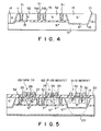
- An example of substrate 20 in which elements are formed and a method for forming elements in substrate 20 are explained with reference to Figs. 4 and 5.
- Fig. 4 shows substrate 20 on which substrate surface etching pattern 21 is formed and which has been subjected to the element isolation process.
- a plurality of grooves 51 of 4 to 5 ⁇ m width are formed by the RIE method to reach insulation film 13 from the substrate surface in first silicon substrate 11, for example, N-type silicon substrate 11 having thickness b of 20 ⁇ m.
- thermal oxide film 51a is formed on the surface of grooves 51
- polysilicon layer 51b is formed in grooves 51 to a thickness of 4 to 5 ⁇ m so as to attain a flat surface.
- the region surrounded by thermal oxide film 13 and groove 51 formed by the RIE method is electrically isolated from the remaining region to form island region 52.
- Fig. 5 shows an example in which function elements are formed in substrate 20 of Fig. 4. Function elements which do not require high withstanding voltage are formed in island region 52.
- NPN transistor 63 having emitter 29, collector 27 and base 28 is formed in one of island regions 52 and P-channel MOSFET 62 having gate 26, drain 25 and source 24 is formed in another island region 52.
- D-MOSFET 61 acting as a power element having base 30, source 31 and gate 32 is formed in epitaxial layer 14 by a known method.
- Layer 23 formed in second semiconductor substrate 12 is an N-type silicon layer of high impurity concentration or metal layer, for example, and serves as a current passage or an electrode.
- reference numeral 33 denotes an insulative protection film.
- thickness a of epitaxial region 14 is larger than thickness b of N-type silicon layer 11.
- thickness a and b are different from each other by the thickness of insulation film 13.
- the structure shown in Fig. 6A can be obtained by effecting the diffusion step shown in Fig. 3H after the step of Fig. 3E, effecting the step of Fig.
- Fig. 6F for removing insulation film 13, and forming epitaxial layer 14 by the epitaxial growth method without effecting the step of Fig. 3G.
- impurity layer 15 surrounds epitaxial layer 14.
- the structure of Fig. 6B can be obtained by effecting the step of Fig. 3H without effecting the step of Fig. 3G for etching second semiconductor substrate 12.
- impurity layer 15 is formed to have a higher impurity concentration than the surrounding regions, but it is also possible to form impurity layer 15 so as to have a lower impurity concentration than the surrounding regions.
- impurity layer 15 is etched at an etching rate different from that of first semiconductor substrate 11 and epitaxial layer 14 when the surface of semiconductor substrate 11 is etched.
- impurity layer 15 it is possible to form impurity layer 15 by using P-type impurity region as the modification of the structure shown in Figs. 2 and 6.
- impurity layer 15 is formed of P-type, epitaxial region 14 is isolated from semiconductor substrate 11 by a PN junction formed of P+-type region 15 and the adjacent N-type region. Thus, it becomes unnecessary to form complicated trench isolation 51, and therefore an element isolation can be easily attained.
- Figs. 7A and 7B show another embodiment of this invention.
- pattern 41 having the same plane configuration as etched portion 17 is formed on the back surface of substrate 12 instead of impurity layer 15.
- Pattern 41 is formed by an etching process, for example.
- Fig. 7B in a case where elements are formed in epitaxial layer 14 or the like after the substrate surface is etched or polished, it is possible to form the elements in the surface area of the substrate while observing the location of embedded oxide film 13 based on the location of pattern 41.
- this method will be practically inconvenient in comparison with the case of Fig. 2.
- first semiconductor substrate 11 and second semiconductor substrate 12 are the same.
- this invention is not limited to this case. That is, two semiconductor substrates having different conductivity types can be bonded.
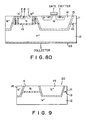
- an embodiment in which two semiconductor substrates having different conductivity types can be bonded and an IGBT is formed in the substrate is explained with reference to Figs. 8A to 8D.
- the conductivity type of second semiconductor substrate 12 and P+-type In this embodiment, the conductivity type of second semiconductor substrate 12 and P+-type.
- First semiconductor substrate 11 of N-type and second semiconductor substrate of P-type are subjected to the steps similar to those of Figs. 3A to 3F so as to attain the semiconductor structure shown in Fig. 8A.
- Fig. 8B N+-type epitaxial layer 15 with a thickness of approx. 15 ⁇ m is formed around etched portion 17 of semiconductor substrate 11.
- layers 16 and 18 are removed, and N-type epitaxial layer is formed on impurity layer 15.
- the substrate surface is polished to make the surface flat.
- isolation structure 51 is formed in first semiconductor substrate 11 to form island region 52.
- an IGBT controlling PNP transistor is formed in island region 52, and an insulated gate and an emitter are formed in epitaxial layer 14 in a well known manner to complete the IGBT.
- Conductive layer 23 formed on second semiconductor substrate 12 of P+-type serves as a collector electrode.
- the IGBT is formed by forming an N+-type epitaxial layer on a P+-type substrate, and forming an N-type layer thereon by the epitaxial growth method.
- the IGBT can be easily constituted by using the composite substrate.
- impurity layer 15 is formed by diffusing impurity into semiconductor substrates 11 and 12.
- impurity layer 15 it is possible to form impurity layer 15 by the epitaxial growth method as shown in Fig. 9.
- insulation films 13a and 13b are formed on first and second semiconductor substrates 11 and 12. However, it is possible to bond the first and second semiconductor substrates to each other after an insulation film is formed on one of the first and second semiconductor substrates.
Landscapes
- Element Separation (AREA)
- Recrystallisation Techniques (AREA)
- Metal-Oxide And Bipolar Metal-Oxide Semiconductor Integrated Circuits (AREA)
- Bipolar Transistors (AREA)
Applications Claiming Priority (2)
| Application Number | Priority Date | Filing Date | Title |
|---|---|---|---|
| JP465/88 | 1988-01-05 | ||
| JP63000465A JPH01179342A (ja) | 1988-01-05 | 1988-01-05 | 複合半導体結晶体 |
Publications (3)
| Publication Number | Publication Date |
|---|---|
| EP0323856A2 true EP0323856A2 (de) | 1989-07-12 |
| EP0323856A3 EP0323856A3 (de) | 1991-02-20 |
| EP0323856B1 EP0323856B1 (de) | 1997-06-04 |
Family
ID=11474545
Family Applications (1)
| Application Number | Title | Priority Date | Filing Date |
|---|---|---|---|
| EP89100183A Expired - Lifetime EP0323856B1 (de) | 1988-01-05 | 1989-01-05 | Substratsstruktur für zusammengesetztes Halbleiterbauelement |
Country Status (5)
| Country | Link |
|---|---|
| US (1) | US4985745A (de) |
| EP (1) | EP0323856B1 (de) |
| JP (1) | JPH01179342A (de) |
| KR (1) | KR910010220B1 (de) |
| DE (1) | DE68928087T2 (de) |
Cited By (7)
| Publication number | Priority date | Publication date | Assignee | Title |
|---|---|---|---|---|
| EP0398468A3 (de) * | 1989-05-16 | 1991-03-13 | Kabushiki Kaisha Toshiba | Dielektrisch isoliertes Substrat und Halbleiteranordnung mit diesem Substrat |
| EP0328331A3 (de) * | 1988-02-08 | 1991-03-20 | Kabushiki Kaisha Toshiba | Halbleiteranordnung und Verfahren zu dessen Herstellung |
| EP0444370A1 (de) * | 1989-12-29 | 1991-09-04 | Telemecanique | Halbleiteranordnung mit einem verdünnten aktiven Bereich und Herstellungsverfahren dafür |
| US5049968A (en) * | 1988-02-08 | 1991-09-17 | Kabushiki Kaisha Toshiba | Dielectrically isolated substrate and semiconductor device using the same |
| US5332920A (en) * | 1988-02-08 | 1994-07-26 | Kabushiki Kaisha Toshiba | Dielectrically isolated high and low voltage substrate regions |
| EP0653785A3 (de) * | 1993-11-17 | 1997-07-09 | Nippon Denso Co | Dielektrisch isolierte Halbleiteranordnung. |
| EP0813248A2 (de) * | 1996-06-12 | 1997-12-17 | Kabushiki Kaisha Toshiba | Dielektrisch isolierte integrierte Schaltung zusammen mit einer Überspannungsschutzschaltung und Herstellungsverfahren |
Families Citing this family (16)
| Publication number | Priority date | Publication date | Assignee | Title |
|---|---|---|---|---|
| US5089863A (en) * | 1988-09-08 | 1992-02-18 | Mitsubishi Denki Kabushiki Kaisha | Field effect transistor with T-shaped gate electrode |
| US5272100A (en) * | 1988-09-08 | 1993-12-21 | Mitsubishi Denki Kabushiki Kaisha | Field effect transistor with T-shaped gate electrode and manufacturing method therefor |
| US5543646A (en) * | 1988-09-08 | 1996-08-06 | Mitsubishi Denki Kabushiki Kaisha | Field effect transistor with a shaped gate electrode |
| US5416354A (en) * | 1989-01-06 | 1995-05-16 | Unitrode Corporation | Inverted epitaxial process semiconductor devices |
| JPH03129854A (ja) * | 1989-10-16 | 1991-06-03 | Toshiba Corp | 半導体装置の製造方法 |
| US5102809A (en) * | 1990-10-11 | 1992-04-07 | Texas Instruments Incorporated | SOI BICMOS process |
| JP2609753B2 (ja) * | 1990-10-17 | 1997-05-14 | 株式会社東芝 | 半導体装置 |
| WO1993026041A1 (en) * | 1992-06-17 | 1993-12-23 | Harris Corporation | Bonded wafer processing |
| US5260233A (en) * | 1992-11-06 | 1993-11-09 | International Business Machines Corporation | Semiconductor device and wafer structure having a planar buried interconnect by wafer bonding |
| JP3116609B2 (ja) * | 1992-11-25 | 2000-12-11 | 日本電気株式会社 | 半導体装置の製造方法 |
| EP0661735B1 (de) * | 1993-12-29 | 2001-03-07 | Consorzio per la Ricerca sulla Microelettronica nel Mezzogiorno | Verfahren zur Herstellung integrierter Schaltungen, insbesondere intelligenter Leistungsanordnungen |
| JP3396553B2 (ja) * | 1994-02-04 | 2003-04-14 | 三菱電機株式会社 | 半導体装置の製造方法及び半導体装置 |
| JP3595182B2 (ja) * | 1999-02-10 | 2004-12-02 | 沖電気工業株式会社 | 半導体装置の製造方法 |
| US6555891B1 (en) | 2000-10-17 | 2003-04-29 | International Business Machines Corporation | SOI hybrid structure with selective epitaxial growth of silicon |
| JP2002217282A (ja) * | 2001-01-19 | 2002-08-02 | Mitsubishi Electric Corp | 半導体装置及びその製造方法 |
| JP2005244020A (ja) * | 2004-02-27 | 2005-09-08 | Toshiba Corp | 半導体装置及びその製造方法 |
Family Cites Families (19)
| Publication number | Priority date | Publication date | Assignee | Title |
|---|---|---|---|---|
| JPS5334483A (en) * | 1977-09-09 | 1978-03-31 | Hitachi Ltd | Substrate for semiconductor integrating circuit |
| US4261003A (en) * | 1979-03-09 | 1981-04-07 | International Business Machines Corporation | Integrated circuit structures with full dielectric isolation and a novel method for fabrication thereof |
| US4283235A (en) * | 1979-07-27 | 1981-08-11 | Massachusetts Institute Of Technology | Dielectric isolation using shallow oxide and polycrystalline silicon utilizing selective oxidation |
| FR2472268A1 (fr) * | 1979-12-21 | 1981-06-26 | Thomson Csf | Procede de formation de caisson dans des circuits integres |
| US4408386A (en) * | 1980-12-12 | 1983-10-11 | Oki Electric Industry Co., Ltd. | Method of manufacturing semiconductor integrated circuit devices |
| JPS57133637A (en) * | 1981-02-13 | 1982-08-18 | Hitachi Ltd | Semiconductor integrated circuit device |
| US4661832A (en) * | 1982-06-30 | 1987-04-28 | International Business Machines Corporation | Total dielectric isolation for integrated circuits |
| US4501060A (en) * | 1983-01-24 | 1985-02-26 | At&T Bell Laboratories | Dielectrically isolated semiconductor devices |
| US4494303A (en) * | 1983-03-31 | 1985-01-22 | At&T Bell Laboratories | Method of making dielectrically isolated silicon devices |
| JPS6081839A (ja) * | 1983-10-12 | 1985-05-09 | Fujitsu Ltd | 半導体装置の製造方法 |
| EP0156964A1 (de) * | 1983-11-18 | 1985-10-09 | Motorola, Inc. | Anordnung und Verfahren zur Isolierung durch PN-Übergang |
| JPS60113455A (ja) * | 1983-11-24 | 1985-06-19 | Hitachi Ltd | 半導体集積回路装置 |
| US4523370A (en) * | 1983-12-05 | 1985-06-18 | Ncr Corporation | Process for fabricating a bipolar transistor with a thin base and an abrupt base-collector junction |
| DE3583183D1 (de) * | 1984-05-09 | 1991-07-18 | Toshiba Kawasaki Kk | Verfahren zur herstellung eines halbleitersubstrates. |
| JPS61184843A (ja) * | 1985-02-13 | 1986-08-18 | Toshiba Corp | 複合半導体装置とその製造方法 |
| US4601779A (en) * | 1985-06-24 | 1986-07-22 | International Business Machines Corporation | Method of producing a thin silicon-on-insulator layer |
| JPS6276645A (ja) * | 1985-09-30 | 1987-04-08 | Toshiba Corp | 複合半導体結晶体構造 |
| JPH077798B2 (ja) * | 1986-01-31 | 1995-01-30 | 日本電信電話株式会社 | 同一平面上に互いに分離しかつ複数の材料からなる島領域を有する複合基板の作製方法 |
| US4784970A (en) * | 1987-11-18 | 1988-11-15 | Grumman Aerospace Corporation | Process for making a double wafer moated signal processor |
-
1988
- 1988-01-05 JP JP63000465A patent/JPH01179342A/ja active Pending
-
1989
- 1989-01-03 US US07/293,026 patent/US4985745A/en not_active Expired - Lifetime
- 1989-01-05 EP EP89100183A patent/EP0323856B1/de not_active Expired - Lifetime
- 1989-01-05 KR KR1019890000035A patent/KR910010220B1/ko not_active Expired
- 1989-01-05 DE DE68928087T patent/DE68928087T2/de not_active Expired - Fee Related
Cited By (8)
| Publication number | Priority date | Publication date | Assignee | Title |
|---|---|---|---|---|
| EP0328331A3 (de) * | 1988-02-08 | 1991-03-20 | Kabushiki Kaisha Toshiba | Halbleiteranordnung und Verfahren zu dessen Herstellung |
| US5049968A (en) * | 1988-02-08 | 1991-09-17 | Kabushiki Kaisha Toshiba | Dielectrically isolated substrate and semiconductor device using the same |
| US5097314A (en) * | 1988-02-08 | 1992-03-17 | Kabushiki Kaisha Toshiba | Dielectrically isolated substrate with isolated high and low breakdown voltage elements |
| US5332920A (en) * | 1988-02-08 | 1994-07-26 | Kabushiki Kaisha Toshiba | Dielectrically isolated high and low voltage substrate regions |
| EP0398468A3 (de) * | 1989-05-16 | 1991-03-13 | Kabushiki Kaisha Toshiba | Dielektrisch isoliertes Substrat und Halbleiteranordnung mit diesem Substrat |
| EP0444370A1 (de) * | 1989-12-29 | 1991-09-04 | Telemecanique | Halbleiteranordnung mit einem verdünnten aktiven Bereich und Herstellungsverfahren dafür |
| EP0653785A3 (de) * | 1993-11-17 | 1997-07-09 | Nippon Denso Co | Dielektrisch isolierte Halbleiteranordnung. |
| EP0813248A2 (de) * | 1996-06-12 | 1997-12-17 | Kabushiki Kaisha Toshiba | Dielektrisch isolierte integrierte Schaltung zusammen mit einer Überspannungsschutzschaltung und Herstellungsverfahren |
Also Published As
| Publication number | Publication date |
|---|---|
| DE68928087D1 (de) | 1997-07-10 |
| JPH01179342A (ja) | 1989-07-17 |
| DE68928087T2 (de) | 1997-10-16 |
| EP0323856A3 (de) | 1991-02-20 |
| US4985745A (en) | 1991-01-15 |
| EP0323856B1 (de) | 1997-06-04 |
| KR890012364A (ko) | 1989-08-26 |
| KR910010220B1 (ko) | 1991-12-21 |
Similar Documents
| Publication | Publication Date | Title |
|---|---|---|
| EP0323856B1 (de) | Substratsstruktur für zusammengesetztes Halbleiterbauelement | |
| EP0217288B1 (de) | Substratstruktur zur Herstellung einer Halbleiterverbundanordnung | |
| US5403769A (en) | Process for producing a semiconductor device | |
| US5004705A (en) | Inverted epitaxial process | |
| EP0182032B1 (de) | SoI-Halbleiteranordnung und Verfahren zu ihrer Herstellung | |
| EP0328331A2 (de) | Halbleiteranordnung und Verfahren zu dessen Herstellung | |
| US5049968A (en) | Dielectrically isolated substrate and semiconductor device using the same | |
| EP0191476A2 (de) | Zusammengesetzte Halbleiteranordnung und Verfahren zu ihrer Herstellung | |
| EP1253645A2 (de) | Lateraler Transistor mit gradierter Basiszone, integrierter Halbleiterschaltkreis und diesbezügliches Herstellungsverfahren | |
| EP0083816B1 (de) | Halbleiteranordnung mit einem Verbindungsmuster | |
| EP0615286B1 (de) | Halbleiteranordnung mit einer Isolationszone | |
| US5332920A (en) | Dielectrically isolated high and low voltage substrate regions | |
| JPH04233764A (ja) | 縦形トランジスタ | |
| US5512774A (en) | Dielectrically isolated substrate and semiconductor device using the same | |
| EP0193116B1 (de) | Verfahren zum Herstellen eines Halbleiterbauelements mit einem Graben | |
| JP3014012B2 (ja) | 半導体装置の製造方法 | |
| EP0490877A2 (de) | Verbindung einer integrierten Schaltung | |
| EP0029552A2 (de) | Verfahren zur Herstellung einer Halbleitervorrichtung | |
| US5406113A (en) | Bipolar transistor having a buried collector layer | |
| EP0637838A2 (de) | Integrierte Schaltung mit selbst-alignierter Isolation | |
| US4740482A (en) | Method of manufacturing bipolar transistor | |
| US20020127823A1 (en) | Reduced substrate capacitance high performance SOI process | |
| EP0398468A2 (de) | Dielektrisch isoliertes Substrat und Halbleiteranordnung mit diesem Substrat | |
| US5763931A (en) | Semiconductor device with SOI structure and fabrication method thereof | |
| JP2979554B2 (ja) | 半導体装置の製造方法 |
Legal Events
| Date | Code | Title | Description |
|---|---|---|---|
| PUAI | Public reference made under article 153(3) epc to a published international application that has entered the european phase |
Free format text: ORIGINAL CODE: 0009012 |
|
| 17P | Request for examination filed |
Effective date: 19890202 |
|
| AK | Designated contracting states |
Kind code of ref document: A2 Designated state(s): DE FR GB IT |
|
| PUAL | Search report despatched |
Free format text: ORIGINAL CODE: 0009013 |
|
| AK | Designated contracting states |
Kind code of ref document: A3 Designated state(s): DE FR GB IT |
|
| 17Q | First examination report despatched |
Effective date: 19940509 |
|
| GRAG | Despatch of communication of intention to grant |
Free format text: ORIGINAL CODE: EPIDOS AGRA |
|
| GRAH | Despatch of communication of intention to grant a patent |
Free format text: ORIGINAL CODE: EPIDOS IGRA |
|
| GRAH | Despatch of communication of intention to grant a patent |
Free format text: ORIGINAL CODE: EPIDOS IGRA |
|
| GRAA | (expected) grant |
Free format text: ORIGINAL CODE: 0009210 |
|
| AK | Designated contracting states |
Kind code of ref document: B1 Designated state(s): DE FR GB IT |
|
| ITF | It: translation for a ep patent filed | ||
| REF | Corresponds to: |
Ref document number: 68928087 Country of ref document: DE Date of ref document: 19970710 |
|
| ET | Fr: translation filed | ||
| PLBE | No opposition filed within time limit |
Free format text: ORIGINAL CODE: 0009261 |
|
| STAA | Information on the status of an ep patent application or granted ep patent |
Free format text: STATUS: NO OPPOSITION FILED WITHIN TIME LIMIT |
|
| 26N | No opposition filed | ||
| REG | Reference to a national code |
Ref country code: GB Ref legal event code: 746 Effective date: 19981002 |
|
| REG | Reference to a national code |
Ref country code: FR Ref legal event code: D6 |
|
| REG | Reference to a national code |
Ref country code: GB Ref legal event code: IF02 |
|
| PGFP | Annual fee paid to national office [announced via postgrant information from national office to epo] |
Ref country code: GB Payment date: 20021231 Year of fee payment: 15 |
|
| PGFP | Annual fee paid to national office [announced via postgrant information from national office to epo] |
Ref country code: FR Payment date: 20030110 Year of fee payment: 15 |
|
| PGFP | Annual fee paid to national office [announced via postgrant information from national office to epo] |
Ref country code: DE Payment date: 20030116 Year of fee payment: 15 |
|
| PG25 | Lapsed in a contracting state [announced via postgrant information from national office to epo] |
Ref country code: GB Free format text: LAPSE BECAUSE OF NON-PAYMENT OF DUE FEES Effective date: 20040105 |
|
| PG25 | Lapsed in a contracting state [announced via postgrant information from national office to epo] |
Ref country code: DE Free format text: LAPSE BECAUSE OF NON-PAYMENT OF DUE FEES Effective date: 20040803 |
|
| GBPC | Gb: european patent ceased through non-payment of renewal fee |
Effective date: 20040105 |
|
| PG25 | Lapsed in a contracting state [announced via postgrant information from national office to epo] |
Ref country code: FR Free format text: LAPSE BECAUSE OF NON-PAYMENT OF DUE FEES Effective date: 20040930 |
|
| REG | Reference to a national code |
Ref country code: FR Ref legal event code: ST |
|
| PG25 | Lapsed in a contracting state [announced via postgrant information from national office to epo] |
Ref country code: IT Free format text: LAPSE BECAUSE OF NON-PAYMENT OF DUE FEES;WARNING: LAPSES OF ITALIAN PATENTS WITH EFFECTIVE DATE BEFORE 2007 MAY HAVE OCCURRED AT ANY TIME BEFORE 2007. THE CORRECT EFFECTIVE DATE MAY BE DIFFERENT FROM THE ONE RECORDED. Effective date: 20050105 |