EP0324650A2 - Taktimpulsgeneratoren - Google Patents
Taktimpulsgeneratoren Download PDFInfo
- Publication number
- EP0324650A2 EP0324650A2 EP89300334A EP89300334A EP0324650A2 EP 0324650 A2 EP0324650 A2 EP 0324650A2 EP 89300334 A EP89300334 A EP 89300334A EP 89300334 A EP89300334 A EP 89300334A EP 0324650 A2 EP0324650 A2 EP 0324650A2
- Authority
- EP
- European Patent Office
- Prior art keywords
- pulse
- timing
- timing pulse
- rom
- output
- Prior art date
- Legal status (The legal status is an assumption and is not a legal conclusion. Google has not performed a legal analysis and makes no representation as to the accuracy of the status listed.)
- Granted
Links
Images




Classifications
-
- G—PHYSICS
- G06—COMPUTING OR CALCULATING; COUNTING
- G06F—ELECTRIC DIGITAL DATA PROCESSING
- G06F1/00—Details not covered by groups G06F3/00 - G06F13/00 and G06F21/00
- G06F1/02—Digital function generators
- G06F1/025—Digital function generators for functions having two-valued amplitude, e.g. Walsh functions
-
- H—ELECTRICITY
- H04—ELECTRIC COMMUNICATION TECHNIQUE
- H04N—PICTORIAL COMMUNICATION, e.g. TELEVISION
- H04N25/00—Circuitry of solid-state image sensors [SSIS]; Control thereof
- H04N25/70—SSIS architectures; Circuits associated therewith
- H04N25/71—Charge-coupled device [CCD] sensors; Charge-transfer registers specially adapted for CCD sensors
- H04N25/745—Circuitry for generating timing or clock signals
Definitions
- This invention relates to timing pulse generators for generating timing pulses by which the operation of a charge coupled device (CCD) imager may be controlled.
- CCD charge coupled device
- FIG. 1 of the accompanying drawings shows an example of a CCD solid state imager of an interline transfer type.
- the CCD device 1 which produces a charge detecting signal at its output terminal 2.
- the CCD device 1 includes a CCD solid state image pickup element 3 which comprises a light receiving section 4, a transfer gate 5, a vertical shift register 6, a horizontal shift register 7 and a charge detecting section 8.
- the vertical shift register 6 is supplied with four-phase vertical transfer clock pulses V1 to V4 from a terminal 9.
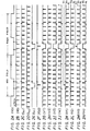
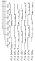
- the waveforms of the four-phase vertical transfer clock pulses V1 to V4 are respectively shown in Figures 2K to 2N of the accompanying drawings. 0n the basis of the four-phase vertical transfer clock pulses V1 to V4, signal charges accumulated in the light receiving section 4 are transferred to the vertical shift register 6 and the signal charges transferred to the vertical shift register 6 are transferred to the horizontal shift register 7.
- the vertical transfer clock pulses V1 and V3 are ternary-value level clock pulses having three levels VL, VH and VT as shown in Figures 2K and 2M, while the vertical transfer clock pulses V2 and V4 are binary-value level clock pulses having two levels VL and VH as shown in Figures 2L and 2N.
- the vertical transfer clock pulse V1 goes to the level VT during the vertical blanking period in odd fields, while the vertical transfer clock pulse V3 goes to the level VT during the vertical blanking period in even fields.
- Figures 2A and 2B of the accompanying drawings illustrate vertical and horizontal synchronising pulses VD and HD, respectively.
- FIG 3 of the accompanying drawings schematically illustrates the relationship between the light receiving section 4, the transfer gate 5 and the vertical shift register 6.
- the electrodes Va, Vb, Vc and Vd at a half pitch of that of alternating light receiving elements SA and SB of the light receiving section 4.
- the electrodes Va and Vb of the vertical shift register 6 are arranged so as to correspond to, for example, the light receiving elements SA of the light receiving section 4.
- the electrodes Vc and Vd of the vertical shift register 6 are arranged so as to correspond to the light receiving elements SB of the light receiving section 4.
- the above-mentioned four-phase vertical transfer clock pulses V1 to V4 are respectively supplied to the electrodes Va to Vd of the vertical shift register 6.
- the signal charges accumulated in the light receiving element SA are transferred through the transfer gate 5 to the portion of the vertical shift register 6 that corresponds to the electrode Va during the period in which the vertical transfer clock pulse V1 goes to the level VT within the vertical blanking period.
- Figures 4A to 4D of the accompanying drawings illustrate conditions in which the vertical transfer clock pulses V1 to V4 are respectively changed in level after a time t0, where the time t0 assumes the transfer timing.
- Figures 5A to 5G of the accompanying drawings illustrate the states of the potential wells and the signal charges under the electrodes Va to Vd at respective times t0 to t6 that are shown in Figures 4A to 4D, respectively.
- the vertical transfer clock pulses V1 and V2 go to the level VH as shown in Figures 4A and 4B while the vertical transfer clock pulses V3 and V4 remain at the level VL as shown in Figures 4C and 4D so that the potential wells under the electrodes Va and Vb are increased in depth.
- the signal charges accumulated under the electrode Va are distributed into the potential wells located under the electrodes Va and Vb.
- the vertical transfer clock pulses V1, V2 and V3 go to the level VH while the vertical transfer clock pulse V4 remains at the level VL so that the potential wells under the electrodes Va, Vb and Vc are increased in depth.
- the signal charges accumulated in the potential wells under the electrodes Va and Vb are further distributed into the potential wells under these electrodes Va, Vb and Vc.
- the vertical transfer clock pulse V1 goes to the level VL
- the vertical transfer clock pulses V2 and V3 remain at the level VH
- the vertical transfer clock pulse V4 remains at the level VL so that the signal charges accumulated in the potential wells under the above-mentioned electrodes Va, Vb and Vc are concentrated in the potential wells under the electrodes Vb and Vc.
- the signal charge accumulated in the light receiving element SB is transferred through the transfer gate 5 to the portion of the vertical shift register 6 corresponding to the electrode Vc during the period in which the vertical transfer clock pulse V3 goes to the level VT within the vertical blanking period. Then, in similar manner to the case of the odd fields, the signal charge is transferred at every scanning line by the vertical shift register 6.
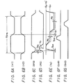
- the horizontal shift register 7 is supplied with two-phase horizontal transfer clock pulses H1 and H2 of one pixel period, for example (as shown in Figures 6A and 6B of the accompanying drawings), 70 ns period from terminals 10 and 11, whereby the signal charges are sequentially delivered from the charge detecting section 8.
- the output terminal of the charge detecting section 8 is connected to ground via a capacitor 12 and is also connected to the source of a pre-charging field-effect-transistor (FET) 13 whose drain is supplied with a DC voltage ER.
- FET 13 receives at its gate a reset pulse PG (shown in Figure 6D of the accompanying drawings) synchronised with the horizontal transfer clock pulses H1 and H2 from a terminal 14 through a capacitor 15.
- PG shown in Figure 6D of the accompanying drawings
- the junction between the charge detecting section 8 and the capacitor 12 is connected to the gate of a source-follower FET 16 and a DC voltage E is supplied to the drain of the FET 16 whose source is connected to the output terminal 2.
- the FET 13 is turned on, so that the capacitor 12 is charged up to the voltage ER. While the voltage of the capacitor 12 should inherently become substantially the value ER, the above reset pulse PG is applied to the capacitor 12 through the gate-source capacity of the FET 13. Thus, the voltage of the capacitor 12 is ER+VP′ during the period in which the reset pulse PG is supplied, where VP′ is the voltage brought about by the jump-in of the pulse PG. When this reset pulse PG disappears, the voltage of the capacitor 12 becomes substantially the above value ER. Reset noise NR is superimposed upon this voltage.
- An output signal SO is detected from the output voltage V0 as follows.
- the reset noise NR superimposed upon the signal level portion and of which the level becomes different at every reset operation is removed.
- the reset noise NR when the reset noise NR is superimposed upon the signal level portion, the reset noise NR of the same level is superimposed upon the reset level portion.
- a broken line shows the condition that the reset noise NR is superimposed upon the reset and signal level portions.
- the output voltage V0 from the output terminal 2 is supplied to a sample and hold circuit 21 which forms part of an output circuit 20.
- a sampling pulse SHD (shown in Figure 6G of the accompanying drawings) corresponding to the signal level period is supplied from a terminal 26 to the sample and hold circuit 21 which samples and holds the signal level portion of the output voltage V0.
- the hold output HS from the sample and hold circuit 21 is supplied to an inverting input terminal of an operational amplifier 22.
- the output voltage V0 is supplied to another sample and hold circuit 23.
- a sampling pulse SHP (shown in Figure 6F of the accompanying drawings) corresponding to the reset level period is supplied from a terminal 27 to the sample and hold circuit 23 which then samples and holds the reset level portion of the output voltage V0.
- the hold output HN1 from the sample and hold circuit 23 is supplied to a further sample and hold circuit 24.
- the sample and hold circuit 24 holds the hold output HN1 in response to the sampling pulse SHD from the terminal 26.
- the hold output HN2 from the sample and hold circuit 24 is supplied to the non-inverting input terminal of the operational amplifier 22.
- Jump-in pulses appear on the hold outputs HS, HN1 and HN2 corresponding to the respective sampling pulses.
- the reset noise NR when the reset noise NR whose level is changed at every reset operation is superimposed upon the output voltage V0 as shown in Figure 6E, although this is not shown, the reset noise NR is also superimposed on the hold outputs HS, HN1 and HN2 of the sample and hold circuits 21, 23 and 24.
- the reset noise NR can be eliminated by calculating the difference between the hold outputs HS and HN1.
- the hold outputs HS and HN1 are produced by sampling the output voltage V0 at the different time points so that a phase difference occurs at the time point when the jump-in pulses appear.
- the difference between the hold outputs HS and HN1 is merely calculated, the jump-in pulses appear as they are.
- the jump-in pulse in the hold output HN2 since the hold output H1 is further sampled and held by the sampling pulse SHD as described above, the jump-in pulse in the hold output HN2 becomes in-phase with the jump-in pulse in the hold output HS.
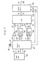
- the vertical transfer clock pulses V1 to V4, the horizontal transfer clock pulses H1, H2, the reset pulse PG and the sampling pulses SHD and SHP which are all supplied to the CCD solid state imager of the example shown in Figure 1 may be produced by the circuit arrangement shown in Figure 7 of the accompanying drawings.
- a timing pulse generator circuit 31 is supplied with a frequency signal S1 from a quartz oscillator 32 having a frequency of, for example, 8 fsc where fsc represents the chrominance subcarrier frequency, 3.58 MHz in the NTSC system.
- the timing pulse generator circuit 31 generates a frequency signal S2 having a frequency of 4 fsc, the frequency signal S2 being supplied to a synchronising signal generator 33.
- the synchronising signal generator 33 responds to the frequency signal S2 to generate a vertical synchronising pulse VD and a horizontal synchronising pulse HD whose waveforms are shown in Figures 2A and 2B. These vertical and horizontal synchronising pulses VD and HD are supplied to the timing pulse generator circuit 31.
- Figures 2C to 2J of the accompanying drawings show other pulses produced by the circuit arrangement of Figure 7.
- the timing pulse generator circuit 31 also produces a sensor-gate signal XSG (shown in Figure 2F) that determines a read-out period in which the signal charges are transferred from the light receiving portion 4 of the CCD solid state image pickup element 3 to the vertical shift register 6, and vertical transfer clock pulses V1′ to V4′ of which the waveforms are respectively shown in Figures 2G to 2J. These pulses are supplied to a vertical clock driver 34.
- the vertical clock driver 34 supplies the vertical transfer clock pulses V1 to V4 (shown in Figures 2K to 2N) to the terminal 9 of the CCD device 1.
- the timing pulse generator circuit 31 further produces a pulse XPG which is shown in Figure 6C of the accompanying drawings.
- This pulse XPG is supplied to a reset pulse driver 35 that is formed by an inverter.
- the reset pulse driver 35 supplies the reset pulse PG (shown in Figure 6D) to the terminal 14 of the CCD device 1.
- the timing pulse generator circuit 31 produces the horizontal transfer clock pulses H1 and H2 (shown in Figures 6A and 6B). These horizontal transfer clock pulses H1 and H2 are supplied to the terminals 10 and 11 of the CCD device 1 via a horizontal clock driver 36.
- the timing pulse generator circuit 31 generates the sampling pulses SHP and SHD (shown in Figures 6F and 6G) which are then supplied to the respective terminals 27 and 26 of the output circuit 20.
- the reference TPG represents the delay time brought about by the reset pulse driver 35
- the references TIM1 and TIM2 in Figure 6E represent delay times brought about by the CCD device 1.
- the circuit for generating the timing pulses such as the vertical transfer clock pulses V1′ to V4′, the sensor-gate signal XSG and the like is formed by, for example, a logic circuit.
- the generated timing pulses are uniquely determined by the logic circuit arrangement, so that if the timing pulses to be generated are modified or corrected, the above-mentioned circuit has to be re-designed to include the modification or correction. This causes difficulties when different timing pulses are required.
- timing pulses may be generated by the use of a read only memory (ROM) so that the timing pulses can be readily modified or corrected without cumbersome re-design.
- ROM read only memory
- the timing pulse repeating in the horizontal direction and the timing pulse repeating in the vertical direction are derived from the common ROM 42 so that the capacity of the ROM 42 has to be relatively large.
- the ROM 42 requires a capacity of N x 238875 bits to generate N timing pulses, where N is a positive integer.
- the capacity of the ROM 42 has to be selected to be the nearest power of two which is more than 238875 bits, in this example, 262144 218) bits corresponding to one timing pulse, wherein if the address counter can specify 262144 addresses, the counter 41 should be an 18-bit counter.
- the above previously-proposed technique needs a very large capacity ROM and a large scale counter.
- a timing pulse generator for generating at least a first timing pulse with a vertical scanning frequency and a second timing pulse with a horizontal scanning frequency, both of said first and second timing pulses being used for controlling a charge coupled device imager, said timing pulse generator comprising: a first address counter for counting a first reference pulse having the horizontal scanning frequency; first read only memory means supplied with the output of said first address counter as a read out address control signal and for generating said first timing pulse; a second address counter for counting a second reference pulse having a frequency higher than that of said horizontal scanning frequency; second read only memory means supplied with the output of said second address counter as a read out address control signal and for generating said second timing pulse; and clock signal generating means for generating clock signals in accordance with said first and second timing pulses.
- a timing pulse generator circuit in which the memory capacities can be reduced considerably compared to the previous proposal.
- FIG 9 shows a timing pulse generator circuit 60 embodying the present invention.
- An oscillator 51 produces a frequency signal S1 having a frequency of, for example, 8 fsc and this frequency signal S1 is supplied to a terminal 61 of the timing pulse generator circuit 60.
- the timing pulse generator circuit 60 receives at its terminals 62, 63 a vertical synchronising pulse VD and a horizontal synchronising pulse HD from a synchronising signal generator (not shown). These vertical and horizontal synchronising pulses VD and HD are supplied to a synchronising circuit 64 within the timing pulse generator circuit 60.
- the waveforms of these vertical and horizontal synchronising pulses VD and HD are shown in Figures 2A and 2B.
- the circuit 60 includes a horizontal read only memory (ROM) 65.
- the frequency signal S1 applied to the terminal 61 is supplied through a half frequency divider 66 to a half frequency divider 67 which produces a frequency signal S2 having a frequency of 2 fsc.
- This frequency signal S2 is supplied to the horizontal ROM 65 as a clock pulse CLKH.
- the synchronising circuit 64 produces a reset pulse PRH of the horizontal period, and this reset pulse PRH is supplied to the horizontal ROM 65.
- the horizontal ROM 65 produces pulses SH1 and SH2 that are repeated at every horizontal period as shown in Figures 2C and 2D, and a pulse SH3 which is used to specify the period in which the horizontal transfer clock pulses H1 and H2 are not produced during the vertical transfer period.
- the horizontal ROM 65 may in practice be constructed as, for example, shown in Figure 10.
- a 7-bit counter 651 which forms an address counter.
- the clock pulse CLKH from the frequency divider 67 is supplied to the clock terminal CK of the counter 651 and the reset pulse PRH is supplied to the reset terminal RE thereof.
- the 7-bit count output from the counter 651 is supplied to a ROM 652 as an address signal.
- Data of the timing pulses repeated in the horizontal period are written in the respective addresses of the ROM 652.
- a control signal (not shown) derived from, for example, the synchronising circuit 64 may control the count operation of the counter 651 so that the data are read out from the ROM 652 at a corresponding timing.
- the horizontal ROM 65 may be constructed as, for example, shown in Figure 11.
- an 8-bit counter 651′ receives at its clock terminal CK the clock pulse CLKH and at its reset terminal RE the reset pulse PRH.
- the 8-bit counter 651′ is further supplied with data DCK that indicates the number n of the clock pulse CLKH in order to determine the duration of the interval.
- the 8-bit counter 651′ is set in the n-scale counter mode to produce a carry output each time it counts n clock pulses.
- a 5-bit counter 652′ which receives at its clock terminal CK the carry output from the 8-bit counter 651′.
- the reset pulse PRH is supplied to the reset terminal RE of the 5-bit counter 652′ whose 5-bit count output is supplied to an address ROM 653′ and a data ROM 654′ as an address signal.
- the 8-bit data DCK is written in the respective addresses of the address ROM 653′.
- This 8-bit data DCK indicates the number n of the clock pulses CLKH which determine the duration of the interval from a certain time point where the timing pulse is changed to the next time point.
- the data of the timing pulses only the data at the change of the timing pulse is written in the respective address of the data ROM 654′
- the data DCK from the address ROM 653′ is supplied to the above-mentioned 8-bit counter 651′.
- the 5-bit counter 652′ produces the count output "X+1" and the address ROM 653′ produces the data DCK of "15", setting the 8-bit counter 651′ in the 15-scale counter mode.
- the timing pulses P1 and P2 from the data ROM 654′ go to the high level "1” and the low level “0", respectively.
- the 8-bit counter 651′ is set in the 15-scale counter mode so that at a time point T3 when the 8-bit counter 651′ has been supplied with 15 clock pulses CLKH, it produces a carry output.
- the 5-bit counter 652′ produces the count output "X+2" and the address ROM 653′ produces the data DCK of "6" so that the 8-bit counter 651′ is set in the 6-scale counter mode.
- the timing pulses P1 and P2 derived from the data ROM 654′ both go to the low level "0".
- the data ROM 654′ produces the timing pulses P1 and P2 whose waveforms are shown in Figures 12A and 12B, respectively.
- the horizontal ROM 65 is modified as described above in connection with the example of Figure 11, the horizontal ROM 65 can produce the pulses SH1, SH2 and SH3.
- the horizontal ROM 65 might be formed as, for example, shown in Figure 15.
- an 8-bit counter 651 ⁇ which receives at its clock terminal CK the clock pulse CLKH and at its reset terminal RE the reset pulse PRH.
- the counter 651 ⁇ supplies its 8-bit count output to a comparator 655 ⁇ .
- the comparator 655 ⁇ is supplied with the data DCK from the address ROM 653′
- the comparator 655 ⁇ produces, when the count output from the counter 651 ⁇ coincides with the data DCK, a coincidence detection pulse.
- the coincidence detection pulse is supplied to the clock terminal CK of the 5-bit counter 652′.
- the counter 651 ⁇ is reset every time when the coincidence detection pulse is produced.
- Other portions of the circuit are arranged similarly to those of the example shown in Figure 11.
- circuit arrangement shown in the example of Figure 15 can be operated similarly to that of the example shown in Figure 11.
- a vertical ROM 69 is provided.
- the synchronising circuit 64 produces a clock pulse CLKV of horizontal period and a reset pulse PRV of frame period.
- the clock pulse CLKV and the reset pulse PRV are supplied to the vertical ROM 69, which produces a pulse SV1 that is repeated in the vertical period.
- the pulse SV1 goes to a low level in correspondence with the read-out period of the CCD solid state image pickup element 3 in the odd and even fields, as shown in Figure 2E.
- the vertical ROM 69 may be constructed as, for example, shown in Figure 16.
- a 5-bit counter 691 which forms an address counter.
- the 5-bit counter 691 receives at its clock terminal CK the clock pulse CLKV and at its reset terminal RE the reset pulse PRV.
- the 5-bit count output from the 5-bit counter 691 is supplied to a ROM 692 as an address signal.
- Data of timing pulses repeated in the vertical period is written in each of the addresses of the ROM 692.
- the relation of 525 lines/frame is established so that data of 525 bits are needed to produce one timing pulse.
- the timing pulses are changed during the vertical blanking period so that, in this embodiment, only data preceding and subsequent to the change of timing pulse are written in the ROM 692.
- data of 32 bits have to be written in the ROM 692 in order to produce one timing pulse.
- the address counter is formed of the 5-bit counter 691 as described above.
- the pulses SH1 and SH2 from the horizontal ROM 65 and the pulse SV1 from the vertical ROM 69 are supplied to a vertical clock circuit 68.
- the vertical clock circuit 68 produces the vertical transfer clock pulses V1′ to V4′ and the sensor-gate signal XSG which are then supplied to terminals 70 and 71, respectively.
- the waveforms of the vertical clock pulses V1′ to V4′ are shown in Figures 2G to 2J and the waveform of the sensor-gate signal XSG is illustrated in Figure 2F.
- the frequency signal S1 applied to the terminal 61 is divided by a half frequency divider 72 to provide a frequency signal S2′ having a frequency of 4 fsc.
- This frequency signal S2′ is supplied through a gate circuit 73 to a phase adjusting circuit 74.
- the pulse SH3 from the horizontal ROM 65 is supplied to the gate circuit 73 as the gate pulse so that the phase adjusting circuit 74 is prevented from receiving the frequency signal S2′ in the period in which no horizontal transfer clock pulses H1 and H2 are produced within the vertical period.
- the phase adjusting circuit 74 produces the horizontal transfer clock pulses H1 and H2, the reset pulse XPG and the sampling pulses SHP and SHD from the frequency signal S2′.
- the horizontal transfer clock pulses H1 and H2 are illustrated in Figures 6A and 6B
- the reset pulse XPG is illustrated in Figure 6C
- the sampling pulses SHP and SHD are illustrated in Figures 6F and 6G, respectively.
- Their phases are adjusted correspondingly. In this case, the phases of the horizontal transfer clock pulses H1 and H2 are adjusted considering the group delay in the horizontal clock driver which will be described later.
- the phase adjusting section of the phase adjusting circuit 74 may be formed of an inverter series formed of inverters 91 connected in series as shown in Figure 17.
- the phase adjusting section is formed by utilising a propagation delay time of the inverters.
- the characteristics of the respective inverters 91 are selected to be the same.
- the respective wiring or interconnection length between the adjacent inverters 91 is selected to be the same so that the capacity (which is the element that determines the delay time) relating to the output of each inverter 91 is made constant.
- the wiring length is made as short as possible.
- Each of the inverter series is treated as one cell including the layout of the inverters 91 and the wiring length between the inverters 91.
- the respective inverter series of the inverters 91 are located close to each other with the same configuration and the same characteristic.
- the phase adjustment is carried out by changing a point at which the output is produced.
- the reference numeral 92 designates an output buffer.
- the overall structure of the timing pulse generator circuit 60 is formed on the same substrate as an integrated circuit (IC) and the wiring thereof is made in the multilayer interconnection fashion (not shown).
- the interconnection of the phase adjusting section is the interconnection on the topmost layer, and is made of so-called 2Al.
- 2Al so-called 2Al.
- the reset pulse XPG and the sampling pulses SHP and SHD of which the phases are adjusted by the phase adjusting circuit 74 are supplied to terminals 75, 76 and 77, respectively.
- the horizontal transfer clock pulses H1 and H2 of which the phases are adjusted by the phase adjusting circuit 74 are supplied through horizontal clock drivers 781 and 782 to terminals 79 and 80, respectively.
- the horizontal clock drivers 781 and 782 are each formed by connecting inverters I1 to I5 in series as shown in Figure 18.
- each of the inverters I1 to I5 is formed by connecting a P-channel metal oxide semiconductor field-effect-transistor (MOSFET) QP and an N-channel MOSFET QN.
- MOSFET metal oxide semiconductor field-effect-transistor
- the channel width of the FETs QP and QN is gradually increased by about three times (the length of the channel is substantially constant) starting from the inverter I1 and ending with the inverter I5, thereby increasing the driving ability gradually.
- the frequency signal S2 of frequency 4 fsc from the frequency divider 66 is supplied to a terminal 81.
- the pulses SH1, SH2 and SH3 repeating at the horizontal period are derived from the horizontal ROM 65, and the pulse SV1 repeating at the vertical period is derived from the vertical ROM 69, the amounts of data that are written in the ROMs 652, 653′, 654′ and 692 of the horizontal and vertical ROMs 65 and 69 are decreased, and thus the capacities of the ROMs used are reduced compared to those of the previous proposal.
- the horizontal ROM 65 is constructed as shown in Figures 11 and 15 since the inverter data DCK between the changes of the timing pulse is written in the address ROM 653′ and only the data at the changing time of the timing pulse is written in the data ROM 654′, the amount of data to be written can be reduced more, and thus the capacities of the ROMs 653′ and 654′ can be further reduced.
- the overall arrangement of the timing pulse generator circuit 60 is formed as an integrated circuit on the same substrate and multilayer interconnection may be utilised. Also, the interconnection of the phase adjusting circuit 74 is carried out by a so-called 2Al so that the phases of the horizontal transfer clock pulses H1, H2, the reset pulse XPG and the sampling pulses SHP and SHD can be adjusted in accordance with an external circuit condition by changing a piece of the 2Al mask, thus allowing the phase-adjustment to be performed with ease.
- the horizontal clock drivers 781 and 782 are formed on the same substrate on which the timing generator circuit 60 is provided, regardless of the scattering in the temperature characteristics and integrated circuits, the phase relationship between the sampling pulses SHP, SHD and the horizontal transfer clock pulses H1, H2 can be maintained constant. Thus, the sampling operation can be precisely effected by the output circuit 20 by considering only the delay time in the CCD device 1.
- the preset pulse driver 35 may also be formed on the same substrate on which the timing pulse generator 60 is provided. However, if the level of the reset pulse PG is not sufficiently high, the reset will not be sufficiently effected. In this embodiment, the preset pulse driver 35 is not formed on the same substrate on which the timing pulse generator circuit 60 is provided in order to make the level of the reset pulse PG sufficiently high, because the preset pulse driver 35 can be better simplified in circuit arrangement if it is formed as an external circuit operable by a different power source.
Landscapes
- Engineering & Computer Science (AREA)
- Multimedia (AREA)
- Signal Processing (AREA)
- Theoretical Computer Science (AREA)
- Physics & Mathematics (AREA)
- General Engineering & Computer Science (AREA)
- General Physics & Mathematics (AREA)
- Transforming Light Signals Into Electric Signals (AREA)
Applications Claiming Priority (2)
| Application Number | Priority Date | Filing Date | Title |
|---|---|---|---|
| JP6202/88 | 1988-01-14 | ||
| JP63006202A JP2687384B2 (ja) | 1988-01-14 | 1988-01-14 | タイミングパルス発生回路 |
Publications (3)
| Publication Number | Publication Date |
|---|---|
| EP0324650A2 true EP0324650A2 (de) | 1989-07-19 |
| EP0324650A3 EP0324650A3 (de) | 1992-05-20 |
| EP0324650B1 EP0324650B1 (de) | 1996-03-20 |
Family
ID=11631953
Family Applications (1)
| Application Number | Title | Priority Date | Filing Date |
|---|---|---|---|
| EP89300334A Expired - Lifetime EP0324650B1 (de) | 1988-01-14 | 1989-01-13 | Taktimpulsgeneratoren |
Country Status (4)
| Country | Link |
|---|---|
| EP (1) | EP0324650B1 (de) |
| JP (1) | JP2687384B2 (de) |
| KR (1) | KR0137035B1 (de) |
| DE (1) | DE68925984T2 (de) |
Cited By (5)
| Publication number | Priority date | Publication date | Assignee | Title |
|---|---|---|---|---|
| EP0495521A3 (en) * | 1991-01-18 | 1992-09-23 | Sony Corporation | Solid state imager |
| WO1993004477A1 (en) * | 1991-08-14 | 1993-03-04 | Eastman Kodak Company | High speed clock driving circuitry for interline transfer ccd imagers |
| EP0783147A3 (de) * | 1995-12-26 | 1997-12-03 | Tektronix, Inc. | Modulator mit individuell gesetzten Flanken |
| EP0740466A3 (de) * | 1995-04-25 | 2000-01-12 | Sony Corporation | Bildaufnahmeeinheit |
| WO2002029817A3 (en) * | 2000-10-06 | 2002-12-27 | Koninkl Philips Electronics Nv | Upscaled clock feeds memory to make parallel waves |
Families Citing this family (1)
| Publication number | Priority date | Publication date | Assignee | Title |
|---|---|---|---|---|
| US7420606B2 (en) * | 2003-07-16 | 2008-09-02 | Matsushita Electric Industrial Co., Ltd. | Timing generator, solid-state imaging device and camera system |
Family Cites Families (2)
| Publication number | Priority date | Publication date | Assignee | Title |
|---|---|---|---|---|
| JPS59190782A (ja) * | 1983-04-14 | 1984-10-29 | Tech Res & Dev Inst Of Japan Def Agency | 固体撮像装置の駆動方法 |
| GB8504161D0 (en) * | 1985-02-19 | 1985-03-20 | Atkinson P | Speed control of induction motors |
-
1988
- 1988-01-14 JP JP63006202A patent/JP2687384B2/ja not_active Expired - Lifetime
- 1988-12-28 KR KR1019880017616A patent/KR0137035B1/ko not_active Expired - Fee Related
-
1989
- 1989-01-13 DE DE68925984T patent/DE68925984T2/de not_active Expired - Fee Related
- 1989-01-13 EP EP89300334A patent/EP0324650B1/de not_active Expired - Lifetime
Cited By (6)
| Publication number | Priority date | Publication date | Assignee | Title |
|---|---|---|---|---|
| EP0495521A3 (en) * | 1991-01-18 | 1992-09-23 | Sony Corporation | Solid state imager |
| US5233430A (en) * | 1991-01-18 | 1993-08-03 | Sony Corporation | Solid state imager wherein the horizontal transfer is accomplished with first and second clock voltages and the cross-over point between the voltages is above the medium level between the peak values of the voltages |
| WO1993004477A1 (en) * | 1991-08-14 | 1993-03-04 | Eastman Kodak Company | High speed clock driving circuitry for interline transfer ccd imagers |
| EP0740466A3 (de) * | 1995-04-25 | 2000-01-12 | Sony Corporation | Bildaufnahmeeinheit |
| EP0783147A3 (de) * | 1995-12-26 | 1997-12-03 | Tektronix, Inc. | Modulator mit individuell gesetzten Flanken |
| WO2002029817A3 (en) * | 2000-10-06 | 2002-12-27 | Koninkl Philips Electronics Nv | Upscaled clock feeds memory to make parallel waves |
Also Published As
| Publication number | Publication date |
|---|---|
| KR0137035B1 (ko) | 1998-04-28 |
| EP0324650A3 (de) | 1992-05-20 |
| JPH01181383A (ja) | 1989-07-19 |
| KR890012480A (ko) | 1989-08-26 |
| DE68925984T2 (de) | 1996-08-08 |
| DE68925984D1 (de) | 1996-04-25 |
| EP0324650B1 (de) | 1996-03-20 |
| JP2687384B2 (ja) | 1997-12-08 |
Similar Documents
| Publication | Publication Date | Title |
|---|---|---|
| KR940008178B1 (ko) | 샘플홀드 회로 및 그것을 이용한 액정디스플레이 장치 | |
| EP0202912A2 (de) | Halbleiterspeicheranordnung in Schieberegisterform mit einem zweiphasigen Taktsignal | |
| EP0324650B1 (de) | Taktimpulsgeneratoren | |
| JP2736121B2 (ja) | 電荷転送装置及び固体撮像装置 | |
| US5515103A (en) | Image signal processing apparatus integrated on single semiconductor substrate | |
| EP0599200A2 (de) | Festkörperbildaufnahmevorrichtung und Verfahren zu ihrem Betrieb | |
| JP2943750B2 (ja) | タイミングパルス発生回路 | |
| EP0282279B1 (de) | Vorrichtung zur Kompression und/oder Dehnung einer Zeitbasis | |
| US4379222A (en) | High speed shift register | |
| JPS59229779A (ja) | 直・並・直形集積メモリ回路 | |
| EP0296682A1 (de) | Bildaufnahmeanordnung mit einem Festkörpersensor und einem elektronischen Verschluss | |
| JP3204197B2 (ja) | Ccd固体撮像装置 | |
| JP2629226B2 (ja) | タイミングパルス発生回路 | |
| JP2825489B2 (ja) | タイミングパルス発生回路 | |
| US5731833A (en) | Solid-state image pick-up device with reference level clamping and image pick-up apparatus using the same | |
| JPH01181384A (ja) | パルス発生回路 | |
| US6885401B1 (en) | Clock signal generator for solid-state imaging apparatus | |
| JPH0723299A (ja) | 駆動パルス生成回路 | |
| JP3454369B2 (ja) | 撮像装置 | |
| JPH0520891A (ja) | Ccd撮像素子 | |
| JP3859294B2 (ja) | 固体撮像装置 | |
| JPH0748830B2 (ja) | 固体撮像装置 | |
| JP3033299B2 (ja) | 固体撮像装置の駆動回路 | |
| EP0289088A1 (de) | Ladungsverschiebeschaltung | |
| EP0364038A1 (de) | Steuerungstaktwellenform für Festkörpersbildsensoren |
Legal Events
| Date | Code | Title | Description |
|---|---|---|---|
| PUAI | Public reference made under article 153(3) epc to a published international application that has entered the european phase |
Free format text: ORIGINAL CODE: 0009012 |
|
| AK | Designated contracting states |
Kind code of ref document: A2 Designated state(s): DE FR GB NL |
|
| PUAL | Search report despatched |
Free format text: ORIGINAL CODE: 0009013 |
|
| AK | Designated contracting states |
Kind code of ref document: A3 Designated state(s): DE FR GB NL |
|
| 17P | Request for examination filed |
Effective date: 19921005 |
|
| 17Q | First examination report despatched |
Effective date: 19940812 |
|
| GRAA | (expected) grant |
Free format text: ORIGINAL CODE: 0009210 |
|
| AK | Designated contracting states |
Kind code of ref document: B1 Designated state(s): DE FR GB NL |
|
| REF | Corresponds to: |
Ref document number: 68925984 Country of ref document: DE Date of ref document: 19960425 |
|
| ET | Fr: translation filed | ||
| PLBE | No opposition filed within time limit |
Free format text: ORIGINAL CODE: 0009261 |
|
| STAA | Information on the status of an ep patent application or granted ep patent |
Free format text: STATUS: NO OPPOSITION FILED WITHIN TIME LIMIT |
|
| 26N | No opposition filed | ||
| REG | Reference to a national code |
Ref country code: GB Ref legal event code: IF02 |
|
| PGFP | Annual fee paid to national office [announced via postgrant information from national office to epo] |
Ref country code: NL Payment date: 20050103 Year of fee payment: 17 |
|
| PGFP | Annual fee paid to national office [announced via postgrant information from national office to epo] |
Ref country code: DE Payment date: 20050106 Year of fee payment: 17 |
|
| PGFP | Annual fee paid to national office [announced via postgrant information from national office to epo] |
Ref country code: FR Payment date: 20050110 Year of fee payment: 17 |
|
| PGFP | Annual fee paid to national office [announced via postgrant information from national office to epo] |
Ref country code: GB Payment date: 20050112 Year of fee payment: 17 |
|
| PG25 | Lapsed in a contracting state [announced via postgrant information from national office to epo] |
Ref country code: GB Free format text: LAPSE BECAUSE OF NON-PAYMENT OF DUE FEES Effective date: 20060113 |
|
| PG25 | Lapsed in a contracting state [announced via postgrant information from national office to epo] |
Ref country code: FR Free format text: LAPSE BECAUSE OF NON-PAYMENT OF DUE FEES Effective date: 20060131 |
|
| PG25 | Lapsed in a contracting state [announced via postgrant information from national office to epo] |
Ref country code: NL Free format text: LAPSE BECAUSE OF NON-PAYMENT OF DUE FEES Effective date: 20060801 Ref country code: DE Free format text: LAPSE BECAUSE OF NON-PAYMENT OF DUE FEES Effective date: 20060801 |
|
| GBPC | Gb: european patent ceased through non-payment of renewal fee |
Effective date: 20060113 |
|
| NLV4 | Nl: lapsed or anulled due to non-payment of the annual fee |
Effective date: 20060801 |
|
| REG | Reference to a national code |
Ref country code: FR Ref legal event code: ST Effective date: 20060929 |