EP0325181B1 - Procédé pour fabriquer un émetteur en polysilicium et une grille en polysilicium utilisant la même gravure de polysilicium sur un oxyde à grille mince - Google Patents
Procédé pour fabriquer un émetteur en polysilicium et une grille en polysilicium utilisant la même gravure de polysilicium sur un oxyde à grille mince Download PDFInfo
- Publication number
- EP0325181B1 EP0325181B1 EP89100610A EP89100610A EP0325181B1 EP 0325181 B1 EP0325181 B1 EP 0325181B1 EP 89100610 A EP89100610 A EP 89100610A EP 89100610 A EP89100610 A EP 89100610A EP 0325181 B1 EP0325181 B1 EP 0325181B1
- Authority
- EP
- European Patent Office
- Prior art keywords
- region
- layer
- polysilicon
- emitter
- bipolar
- Prior art date
- Legal status (The legal status is an assumption and is not a legal conclusion. Google has not performed a legal analysis and makes no representation as to the accuracy of the status listed.)
- Expired - Lifetime
Links
Images



Classifications
-
- H—ELECTRICITY
- H10—SEMICONDUCTOR DEVICES; ELECTRIC SOLID-STATE DEVICES NOT OTHERWISE PROVIDED FOR
- H10D—INORGANIC ELECTRIC SEMICONDUCTOR DEVICES
- H10D84/00—Integrated devices formed in or on semiconductor substrates that comprise only semiconducting layers, e.g. on Si wafers or on GaAs-on-Si wafers
- H10D84/40—Integrated devices formed in or on semiconductor substrates that comprise only semiconducting layers, e.g. on Si wafers or on GaAs-on-Si wafers characterised by the integration of at least one component covered by groups H10D12/00 or H10D30/00 with at least one component covered by groups H10D10/00 or H10D18/00, e.g. integration of IGFETs with BJTs
- H10D84/401—Combinations of FETs or IGBTs with BJTs
-
- H—ELECTRICITY
- H10—SEMICONDUCTOR DEVICES; ELECTRIC SOLID-STATE DEVICES NOT OTHERWISE PROVIDED FOR
- H10D—INORGANIC ELECTRIC SEMICONDUCTOR DEVICES
- H10D64/00—Electrodes of devices having potential barriers
- H10D64/01—Manufacture or treatment
- H10D64/013—Manufacture or treatment of electrodes having a conductor capacitively coupled to a semiconductor by an insulator
- H10D64/01302—Manufacture or treatment of electrodes having a conductor capacitively coupled to a semiconductor by an insulator the insulator being formed after the semiconductor body, the semiconductor being silicon
- H10D64/01304—Manufacture or treatment of electrodes having a conductor capacitively coupled to a semiconductor by an insulator the insulator being formed after the semiconductor body, the semiconductor being silicon characterised by the conductor
- H10D64/01306—Manufacture or treatment of electrodes having a conductor capacitively coupled to a semiconductor by an insulator the insulator being formed after the semiconductor body, the semiconductor being silicon characterised by the conductor the conductor comprising a layer of silicon contacting the insulator, e.g. polysilicon
-
- H—ELECTRICITY
- H10—SEMICONDUCTOR DEVICES; ELECTRIC SOLID-STATE DEVICES NOT OTHERWISE PROVIDED FOR
- H10D—INORGANIC ELECTRIC SEMICONDUCTOR DEVICES
- H10D84/00—Integrated devices formed in or on semiconductor substrates that comprise only semiconducting layers, e.g. on Si wafers or on GaAs-on-Si wafers
- H10D84/01—Manufacture or treatment
- H10D84/0107—Integrating at least one component covered by H10D12/00 or H10D30/00 with at least one component covered by H10D8/00, H10D10/00 or H10D18/00, e.g. integrating IGFETs with BJTs
- H10D84/0109—Integrating at least one component covered by H10D12/00 or H10D30/00 with at least one component covered by H10D8/00, H10D10/00 or H10D18/00, e.g. integrating IGFETs with BJTs the at least one component covered by H10D12/00 or H10D30/00 being a MOS device
-
- H—ELECTRICITY
- H10—SEMICONDUCTOR DEVICES; ELECTRIC SOLID-STATE DEVICES NOT OTHERWISE PROVIDED FOR
- H10D—INORGANIC ELECTRIC SEMICONDUCTOR DEVICES
- H10D84/00—Integrated devices formed in or on semiconductor substrates that comprise only semiconducting layers, e.g. on Si wafers or on GaAs-on-Si wafers
- H10D84/01—Manufacture or treatment
- H10D84/02—Manufacture or treatment characterised by using material-based technologies
- H10D84/03—Manufacture or treatment characterised by using material-based technologies using Group IV technology, e.g. silicon technology or silicon-carbide [SiC] technology
- H10D84/038—Manufacture or treatment characterised by using material-based technologies using Group IV technology, e.g. silicon technology or silicon-carbide [SiC] technology using silicon technology, e.g. SiGe
-
- H—ELECTRICITY
- H10—SEMICONDUCTOR DEVICES; ELECTRIC SOLID-STATE DEVICES NOT OTHERWISE PROVIDED FOR
- H10P—GENERIC PROCESSES OR APPARATUS FOR THE MANUFACTURE OR TREATMENT OF DEVICES COVERED BY CLASS H10
- H10P50/00—Etching of wafers, substrates or parts of devices
- H10P50/20—Dry etching; Plasma etching; Reactive-ion etching
- H10P50/28—Dry etching; Plasma etching; Reactive-ion etching of insulating materials
- H10P50/282—Dry etching; Plasma etching; Reactive-ion etching of insulating materials of inorganic materials
- H10P50/283—Dry etching; Plasma etching; Reactive-ion etching of insulating materials of inorganic materials by chemical means
Definitions
- This invention relates to semiconductor devices and, more particularly, to the simultaneous formation of bipolar and metal oxide semiconductor (MOS) devices on the same silicon substrate.
- MOS metal oxide semiconductor
- bipolar devices are fabricated separately from MOS devices because of the structural differences between the two types of devices. This means that a circuit which uses both bipolar and MOS devices must be constructed using discrete chips, which increases the size and cost of the product.
- EP-A-0 196 757 discloses a method defined by the preamble of claim 1.
- bipolar and MOS devices are to be combined, an integrated approach to device fabrication must be devised.
- applying the fabrication techniques used for one type of device to another type of device typically degrades the performance of the other device.
- a common method for making electrical contact to a silicon substrate in a bipolar transistor involves the use of a layer of polysilicon deposited on the surface of the substrate. Electrical contact to the silicon substrate is made through this layer of polysilicon. The resulting structure is termed a "buried contact.”
- the polysilicon/silicon interface layer increases the series resistance through the device. This is insignificant in bipolar devices, because the base of bipolar devices has small current flowing through it, and bipolar devices have intrinsically high resistances.
- MOS devices carry all of the current, so any increase in series resistance significantly affects performance of the devices.
- Series resistance can be improved by increasing the contact area, but with a resulting decrease in yield.
- thin gate oxide layer used in MOS devices is subject to contamination and mechanical damage when subjected to bipolar fabrication methods.
- the present invention is directed to a method of making bipolar and MOS devices simultaneously using a single fabrication process.
- the process according to Claim 1 of the present invention employs the use of buried contacts without significantly affecting the performance of the MOS devices, and a very thin gate oxide layer may be used in the MOS devices without jeopardizing the integrity or performance of the devices.
- a silicon substrate is divided into bipolar and MOS regions.
- a thin layer of gate oxide then is thermally grown on the silicon substrate.
- a thin layer of polysilicon is deposited on the gate oxide layer to protect the gate oxide layer during subsequent processing, and then both the thin polysilicon layer and the gate oxide layer are removed from the bipolar region where the emitter is to be formed.
- the photoresist mask used during the polysilicon etch is retained during the gate oxide etch, and the gate oxide is etched in a buffered oxide etch solution.
- a thick layer of polysilicon then is deposited on the bipolar and MOS regions of the silicon substrate, and the substrate is masked for forming the emitter and gates of the bipolar and MOS devices, respectively, After the emitter and gate locations are masked, the polysilicon is simultaneously etched from the bipolar and MOS regions for forming the respective emitter and gates. Since the polysilicon over the area where the emitter is formed is thinner than the polysilicon over the MOS region, the silicon substrate surrounding the emitter is etched for forming the emitter island. The areas for the base and collector of the bipolar device and the source and drain of the MOS devices are selectively masked during etching of the polysilicon for providing buried contacts to these regions, if desired.
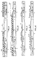
- Figs. 1-16 illustrate the steps of forming a combination bipolar/CMOS device according to the present invention.
- Fig. 1 shows a silicon substrate 4 after having undergone preliminary processing according to conventional methods.
- silicon substrate 4 has been processed to form a bipolar region 8, an NMOS region 12, and a PMOS region 16.
- Bipolar region 8 is intended to be used for forming an NPN transistor
- NMOS region 12 is intended to be used for forming an N-channel MOS device
- PMOS region 16 is intended to be used for forming a P-channel MOS device.
- N+ buried layers 20 and 24 may be formed, for example, by the process disclosed in U.S. -A- 3,648,125 to Douglas L. Peltzer, and assigned to Fairchild Camera and Instrument Corp.
- N-wells 28 and 32 are N-wells 28 and 32, respectively, formed by diffusion of an appropriate N-type impurity, such as phosphorous, into substrate 4 according to well known techniques.
- N+ buried layers 20 and 24 typically have an impurity concentration of approximately 1 x 10²⁰ atoms/cm3 and are approximately 1 »m thick, whereas N-wells 28 and 32 typically have an impurity concentration of approximately 1 x 10¹⁶ atoms/cm3 and a thickness of approximately 0.8 »m.
- CVD chemical vapor deposition
- a layer of photoresist 44 is deposited on silicon nitride layer 40 through a blanket coating, preferably by spinning, to a thickness of approximately 1.5»m.
- the photoresist layer 44 is subjected to a pattern exposure so that development of the photoresist produces portions of photoresist layer 44, as shown in Fig. 2.
- These remaining portions of photoresist layer 44 function as a mask to enable etching of the layer 40 of silicon nitride in the areas not protected by the remaining portions of photoresist layer 44.
- This etching preferably is a dry etch with a plasma, such as SF6. This produces the structure illustrated in Fig. 2.
- semi-recessed isolation oxide (SROX) regions 48, 52, and 56 are formed by thermal oxidation in the presence of dry oxygen or steam.
- the SROX regions 48, 52, and 56 are formed by thermal oxidation in steam at a temperature of 900°C to a thickness of from approximately 5000 angstroms to approximately 6000 angstroms, preferably 5500 angstroms.
- bipolar region 8 is electrically isolated from NMOS region 12 by SROX region 52, and NMOS region 12 is electrically isolated from PMOS region 16 by SROX region 56.
- SROX region 48 separates bipolar region 8 into a collector region 64 and a base/emitter region 68. The remaining portions of photoresist layer 44 are removed by a solvent or oxygen plasma, for example.
- the remaining portions of silicon nitride layer 40 and silicon dioxide layer 36 are removed to produce the structure shown in Fig. 4.
- the portions of silicon nitride layer 40 may be removed by wet etching in orthophosphoric acid, and silicon dioxide layer 36 may be removed by wet etching in hydroflouric acid.
- the next step is to form a thin layer of silicon dioxide 70 on the exposed surfaces of substrate 4.
- Silicon dioxide layer 70 preferably is grown in the same manner as silicon dioxide layer 36, and it has a thickness in the range of from approximately 150 angstroms to 300 angstroms, preferably 170 angstroms. This range has been found by experimentation to be critical in order to avoid contamination and mechanical damage during subsequent processing.
- a thin polycrystalline silicon layer 72 is deposited as a blanket coating over the silicon dioxide layer 70 and the SROX regions 48, 52, and 56.
- the polycrystalline silicon layer 72 is deposited by CVD, and it has a thickness of from approximately 500 angstroms to 1000 angstroms, preferably 700 angstroms. This thickness of polycrystalline silicon layer 72 has been found by experimentation to be critical to protect silicon dioxide layer 70 during subsequent processing.
- a photoresist layer 76 is deposited as a blanket coating over polycrystalline silicon layer 72 in the same manner as photoresist layer 44.
- openings 80 are formed over base/emitter region 68 and over those regions where buried contacts to the silicon substrate are desired. Two such regions are shown.
- the exposed sections of polycrystalline silicon layer 72 are removed by a dry etch.
- the dry etch may be performed with a plasma, such as SF6.
- gate oxide layer 70 are ion-implanted with a P-type impurity, preferably boron, with an energy of 40 KeV to a concentration of approximately 1 x 10¹⁸ atoms/cm3.
- a P-type impurity preferably boron
- This P-type implant forms the initial base region 84 in N-well 28 of bipolar region 8 and the source contact region 85 in PMOS region 16.
- the P-type implant has a negligible effect on the P-type substrate beneath the exposed region in NMOS region 12.
- the exposed portions of gate oxide layer 70 are removed through a buffered oxide etch while maintaining photoresist layer 76 as a mask.
- Photoresist layer 76 then is removed, and a relatively thick polycrystalline silicon layer 74 is deposited as a blanket coating by CVD over the remaining portions of polycrystalline silicon layer 72 and the exposed areas of silicon substrate 4.
- Polycrystalline silicon layer 74 is substantially thicker than polycrystalline silicon layer 72, and preferably has a thickness of from approximately 2200 angstroms to 2800 angstroms, preferably 2500 angstroms.
- a layer of photoresist 77 is deposited and developed to form openings 88 over base/emitter region 68, where an emitter is to be formed, and over NMOS region 12.
- Polycrystalline silicon layers 72 and 74 then are doped by ion implantation to reduce their resistivity.
- an N-type impurity such as arsenic
- the ions are implanted with an energy of 80 KeV to a concentration of from approximately 1 x 10¹⁵ to 1 x 10¹⁶ atoms/cm3. This is to make the conductivity of the exposed polysilicon layers as high as possible to function as a conductor.
- the remaining portions of photoresist layer 77 are removed, and the structure is then annealed at a temperature of from approximately 900°C to 950°C for approximately 30 minutes in a nitrogen atmosphere. This causes diffusion to expand the initial base region 84 and P+ region 85 and to form N+ region 92.
- a photoresist layer 96 is deposited over polysilicon layer 74.
- Photoresist layer 96 is developed to expose all areas of polysilicon layer 74, except over a region 100 which will form the emitter of the bipolar device, over a region 104 which will form the gate of the NMOS device, over a region 106 which will form the gate of the PMOS device, and over the regions of polysilicon layer 74 where buried contacts to the silicon substrate are to be made, e.g. , over SROX region 52.
- the exposed portions of polysilicon layer 74 then are etched by a plasma, such as SF6, until the exposed portions of polysilicon are removed.
- portions of substrate 4 not protected by gate oxide layer 70 are etched to a depth approximately equal to that of the polysilicon layer 72. This occurs in base/emitter region 68 and forms an emitter island 108. Consequently, the thickness of polysilicon layers 72 and 74 in regions 104 and 106, which form the NMOS and PMOS gates, is the same as the depth of polysilicon layer 74 and emitter island 108 in region 100.
- photoresist layer 96 is removed and a photoresist layer 110 is deposited over substrate 4 everywhere except collector region 64 of bipolar region 8 and NMOS region 12.
- a lightly doped drain (LDD) implant is performed with phosphorous ions on the exposed regions at an implantation energy of 40 KeV to a concentration of from approximately 1 x 10¹³ to 1 x 10¹⁴ atoms/cm3.
- photoresist layer 110 is removed and a photoresist layer 114 is deposited over substrate 4.
- Photoresist layer 114 then is developed to form openings 118 over base/emitter region 68 and PMOS region 16.
- a P-type LDD implant is performed, preferably with boron difluoride at an implantation energy of 50 KeV to a concentration of from approximately 1 x 10¹³ to 1 x 10¹⁴, preferably 5 x 10¹³ atoms/cm3. Thereafter, photoresist layer 114 is removed.
- a conformal silicon dioxide layer is deposited by CVD over the entire surface of substrate 4 to a thickness of from approximately 1500 to 4000 angstroms, preferably 2000 angstroms. Silicon dioxide layer 122 then is subjected to an LTO densification by heating at approximately 900°C for approximately 15 minutes.
- silicon dioxide layer 122 is subjected to an anisotropic etch, preferably in a plasma comprising He ⁇ C2F6 ⁇ CHF3 to form spacers 126, 128, 130, 132, 134, 136, 137, 138, 139, 140, 141, and 142.
- a photoresist mask 144 similar to photoresist mask 110, is deposited and developed to expose collector region 64 and NMOS region 12.
- An N-type ion implant then is performed, preferably with arsenic, at an implantation energy of 100 KeV to a concentration of approximately 5 x 10¹⁵ atoms/cm3 for forming the source and drain regions of the NMOS device and the collector of the bipolar device.
- substrate 4 is annealed at a temperature of 900°C for approximately 30 minutes to form N+ collector 145, in bipolar region 8, and N+ source 146 (which merges with N+ region 92) and N+ drain 147 in NMOS region 12.
- a photoresist layer 150 is deposited and developed to form an opening 154 over PMOS region 16, and then a P-type ion implant is performed with boron difluoride at an implantation energy of 50 KeV to a concentration of approximately 3 x 10¹⁵ atoms/cm3 for creating the source and drain of the PMOS device. Then, as shown in Fig. 15, photoresist layer 150 is removed and a final blanket, unmasked P-type implant with BF2 at an implantation energy of 50 KeV to a concentration of 1 x 10¹⁴ atoms/cm3 is performed for forming the extrinsic base of the bipolar device.
- Substrate 4 then is annealed at a temperature of 900° for approximately 40 minutes to form base 155 (which merges with region 84), in bipolar region 8, and P+ source 156 (which merges with P+ region 85) and P+ drain 157 in PMOS region 16.
- the exposed silicon and polysilicon regions are silicided using well known techniques to form silicide layers 173.
- the substrate 4 is covered with a planarizing layer 174 of deposited oxide using well known techniques, such as LTO. Planarizing layer 174 then is etched, and metal contacts 178 are made to the conductive regions also using well known techniques.
Landscapes
- Metal-Oxide And Bipolar Metal-Oxide Semiconductor Integrated Circuits (AREA)
- Bipolar Transistors (AREA)
- Bipolar Integrated Circuits (AREA)
Claims (7)
- Procédé de réalisation d'un émetteur en polysilicium et d'une grille en polysilicium dans un dispositif semi-conducteur comprenant les étapes consistant à :- former par croissance une fine couche (70) d'oxyde de grille sur des régions d'émetteur et de grille d'un substrat en silicium (4),- éliminer la couche d'oxyde de grille de la région d'émetteur du substrat en silicium,- déposer une couche de polysilicium épaisse (74) sur les régions d'émetteur et de grille du substrat en polysilicium,- masquer les régions d'émetteur et de grille pour définir un émetteur et une grille respectives,- graver simultanément des parties de polysilicium des régions d'émetteur et de grille pour former l'émetteur et la grille respectives, caractérisé en ce que avant l'étape d'élimination de l'oxyde de grille, on dépose une mince couche (72) de polysilicium sur la couche d'oxyde de grille qui est ultérieurement éliminée de la région d'émetteur et en ce que lors de l'étape de gravage simultané, le gravage dans la région d'émetteur s'étend dans le substrat sur une quantité correspondant à l'épaisseur de la couche de polysilicium mince.
- Procédé selon la revendication 1 selon lequel l'étape d'élimination de la couche de polysilicium comprend les étapes consistant à :- déposer une couche de résine photosensible (76) comme un revêtement en couverture au-dessus de la couche de polysilicium mince,- développer la couche de résine photosensible pour former une ouverture (80) dans la couche de résine photosensible pour exposer la partie de la couche de polysilicium au-dessous de la région d'émetteur, et- graver la partie exposée de la couche de polysilicium pour exposer la partie de la couche d'oxyde de grille au-dessus de la région d'émetteur.
- Procédé selon la revendication 2 selon lequel l'étape d'élimination de la couche d'oxyde de grille comprend les étapes consistant à :- conserver la couche de résine photosensible (76), et- graver la partie exposée de la couche d'oxyde de grille (70) dans une solution de gravage d'oxyde tamponnée.
- Procédé selon la revendication 3 selon lequel l'étape de croissance de l'oxyde de grille comprend les étapes consistant à :
- former par croissance une couche de dioxyde de silicium (70) sur les régions d'émetteur et de grille du substrat en silicium, le dioxyde de silicium ayant une épaisseur comprise dans la gamme d'approximativement 15 nm (150 angströms) à approximativement 30 nm (300 angströms). - Procédé selon la revendication 4 selon lequel l'étape de dépôt de la couche de polysilicium mince comprend l'étape consistant à déposer une couche de polysilicium (72) jusqu'à obtenir une épaisseur comprise entre approximativement 50 nm (500 angströms) à approximativement 100 nm (1'000 angströms).
- Procédé selon la revendication 5 comprenant en outre les étapes consistant à :- déposer une couche d'oxyde conforme (122) comme revêtement de couverture sur le substrat en silicium (4), et- graver de façon anisotrope la couche conforme de la région bipolaire et de la région MOS.
- Procédé selon l'une des revendications 1 à 6, comprenant les étapes consistant à :- former une région bipolaire (8) dans ledit substrat en silicium pour un dispositif bipolaire, la région bipolaire ayant une première région (64) désignée région de collecteur et une deuxième région (68), la première et la deuxième région étant séparées par une première région d'oxyde de champ (48),- former une région MOS (12, 16) dans le substrat en silicium pour un dispositif MOS, la région MOS étant séparée de la région bipolaire par une deuxième région d'oxyde de champ (52),- former ladite couche d'oxyde de grille (70) sur la région bipolaire et sur la région MOS,- former ladite couche de polysilicium mince sur la région bipolaire et sur la région MOS,- éliminer la couche de polysilicium mince de la deuxième région,- éliminer la couche d'oxyde de grille de la deuxième région,- déposer ladite couche de polysilicium épaisse sur la région bipolaire et sur la région MOS,- masquer une partie de la deuxième région pour former un émetteur,- masquer une partie de la région MOS pour former une grille,- graver simultanément le polysilicium de la région bipolaire et de la région MOS autre que la partie masquée de la région bipolaire et de la région MOS,- éliminer la couche d'oxyde de grille mince de la région de collecteur,- doper la région de collecteur et la région MOS avec un premier type de conductivité,- doper la deuxième région avec un deuxième type de conductivité opposé au type de conductivité de la région de collecteur,- déposer une couche d'oxyde conforme (122) sur la région bipolaire et sur la région MOS, et- graver de façon anisotrope la couche conforme de la région bipolaire et de la région MOS.
Applications Claiming Priority (2)
| Application Number | Priority Date | Filing Date | Title |
|---|---|---|---|
| US14507688A | 1988-01-19 | 1988-01-19 | |
| US145076 | 1988-01-19 |
Publications (3)
| Publication Number | Publication Date |
|---|---|
| EP0325181A2 EP0325181A2 (fr) | 1989-07-26 |
| EP0325181A3 EP0325181A3 (en) | 1990-10-10 |
| EP0325181B1 true EP0325181B1 (fr) | 1995-04-05 |
Family
ID=22511513
Family Applications (1)
| Application Number | Title | Priority Date | Filing Date |
|---|---|---|---|
| EP89100610A Expired - Lifetime EP0325181B1 (fr) | 1988-01-19 | 1989-01-14 | Procédé pour fabriquer un émetteur en polysilicium et une grille en polysilicium utilisant la même gravure de polysilicium sur un oxyde à grille mince |
Country Status (4)
| Country | Link |
|---|---|
| EP (1) | EP0325181B1 (fr) |
| JP (2) | JP2895845B2 (fr) |
| CA (1) | CA1296111C (fr) |
| DE (1) | DE68921995T2 (fr) |
Families Citing this family (10)
| Publication number | Priority date | Publication date | Assignee | Title |
|---|---|---|---|---|
| JPS62274471A (ja) * | 1986-05-23 | 1987-11-28 | Fanuc Ltd | 画像処理装置 |
| JPH03198371A (ja) * | 1989-12-27 | 1991-08-29 | Oki Electric Ind Co Ltd | 半導体装置の製造方法 |
| IT1248534B (it) * | 1991-06-24 | 1995-01-19 | Sgs Thomson Microelectronics | Procedimento per la realizzazione di strutture di calibrazione particolarmente per la taratura di macchine di misura del disallineamento in circuiti integrati in genere. |
| KR930008018B1 (ko) * | 1991-06-27 | 1993-08-25 | 삼성전자 주식회사 | 바이씨모스장치 및 그 제조방법 |
| JPH05226589A (ja) * | 1992-02-17 | 1993-09-03 | Mitsubishi Electric Corp | C−BiCMOS型半導体装置およびその製造方法 |
| FR2702307B1 (fr) * | 1993-03-05 | 1995-08-18 | Itt Ind Gmbh Deutsche | Procédé de fabrication d'un circuit intégré monolithique avec au moins un transistor à effet de champ CMOS et un transistor npn bipolaire. |
| DE4319437C1 (de) * | 1993-03-05 | 1994-05-19 | Itt Ind Gmbh Deutsche | Verfahren zur Herstellung einer monolithisch integrierten Schaltung mit mindestens einem CMOS-Feldeffekttransistor und einem npn-Bipolar-Transistor |
| US5411900A (en) * | 1993-03-05 | 1995-05-02 | Deutsche Itt Industries, Gmbh | Method of fabricating a monolithic integrated circuit with at least one CMOS field-effect transistor and one NPN bipolar transistor |
| DE19523536A1 (de) * | 1994-07-12 | 1996-01-18 | Siemens Ag | Verfahren zur Herstellung von MOS-Transistoren und Bipolartransistoren auf einer Halbleiterscheibe |
| US6448124B1 (en) * | 1999-11-12 | 2002-09-10 | International Business Machines Corporation | Method for epitaxial bipolar BiCMOS |
Family Cites Families (7)
| Publication number | Priority date | Publication date | Assignee | Title |
|---|---|---|---|---|
| JPS6072255A (ja) * | 1983-09-28 | 1985-04-24 | Toshiba Corp | 半導体集積回路装置およびその製造方法 |
| GB8507624D0 (en) * | 1985-03-23 | 1985-05-01 | Standard Telephones Cables Ltd | Semiconductor devices |
| JPH0628296B2 (ja) * | 1985-10-17 | 1994-04-13 | 日本電気株式会社 | 半導体装置の製造方法 |
| JPS6298663A (ja) * | 1985-10-24 | 1987-05-08 | Nec Corp | 半導体集積回路装置 |
| US4735911A (en) * | 1985-12-17 | 1988-04-05 | Siemens Aktiengesellschaft | Process for the simultaneous production of bipolar and complementary MOS transistors on a common silicon substrate |
| DE3680520D1 (de) * | 1986-03-22 | 1991-08-29 | Itt Ind Gmbh Deutsche | Verfahren zum herstellen einer monolithisch integrierten schaltung mit mindestens einem bipolaren planartransistor. |
| JPS62239563A (ja) * | 1986-04-11 | 1987-10-20 | Nec Corp | 半導体装置の製造方法 |
-
1989
- 1989-01-14 DE DE68921995T patent/DE68921995T2/de not_active Expired - Fee Related
- 1989-01-14 EP EP89100610A patent/EP0325181B1/fr not_active Expired - Lifetime
- 1989-01-18 CA CA000588500A patent/CA1296111C/fr not_active Expired - Fee Related
- 1989-01-19 JP JP1008734A patent/JP2895845B2/ja not_active Expired - Fee Related
-
1998
- 1998-10-05 JP JP28286898A patent/JP3165118B2/ja not_active Expired - Lifetime
Also Published As
| Publication number | Publication date |
|---|---|
| DE68921995T2 (de) | 1995-12-07 |
| DE68921995D1 (de) | 1995-05-11 |
| JP3165118B2 (ja) | 2001-05-14 |
| CA1296111C (fr) | 1992-02-18 |
| EP0325181A3 (en) | 1990-10-10 |
| EP0325181A2 (fr) | 1989-07-26 |
| JPH11191597A (ja) | 1999-07-13 |
| JPH023964A (ja) | 1990-01-09 |
| JP2895845B2 (ja) | 1999-05-24 |
Similar Documents
| Publication | Publication Date | Title |
|---|---|---|
| US4752589A (en) | Process for the production of bipolar transistors and complementary MOS transistors on a common silicon substrate | |
| US5424572A (en) | Spacer formation in a semiconductor structure | |
| US5668024A (en) | CMOS device structure with reduced risk of salicide bridging and reduced resistance via use of a ultra shallow, junction extension, ion implantation process | |
| US5082796A (en) | Use of polysilicon layer for local interconnect in a CMOS or BiCMOS technology incorporating sidewall spacers | |
| US5001081A (en) | Method of manufacturing a polysilicon emitter and a polysilicon gate using the same etch of polysilicon on a thin gate oxide | |
| US5336625A (en) | BiCMOS process with low base recombination current bipolar transistors | |
| EP0296627A2 (fr) | Procédé pour manufacturer un dispositif semi-conducteur | |
| US5079177A (en) | Process for fabricating high performance bicmos circuits | |
| JPH04226064A (ja) | 半導体装置用の相互接続体及びその製造方法 | |
| EP0325181B1 (fr) | Procédé pour fabriquer un émetteur en polysilicium et une grille en polysilicium utilisant la même gravure de polysilicium sur un oxyde à grille mince | |
| US5328860A (en) | Method of manufacturing a semiconductor device | |
| JPH09232445A (ja) | 半導体装置およびその製造方法 | |
| US5179031A (en) | Method of manufacturing a polysilicon emitter and a polysilicon gate using the same etch of polysilicon on a thin gate oxide | |
| US5348896A (en) | Method for fabricating a BiCMOS device | |
| US5081518A (en) | Use of a polysilicon layer for local interconnect in a CMOS or BICMOS technology incorporating sidewall spacers | |
| JPH0645343A (ja) | ボロシリケイトガラススペーサを有する半導体装置及びその製造方法 | |
| US5124817A (en) | Polysilicon emitter and a polysilicon gate using the same etch of polysilicon on a thin gate oxide | |
| US5158900A (en) | Method of separately fabricating a base/emitter structure of a BiCMOS device | |
| EP0763256B1 (fr) | Procede de fabrication d'un dispositif a semiconducteur dote d'un circuit bicmos | |
| JP3248305B2 (ja) | BiCMOS半導体装置の製造方法 | |
| EP0398247A2 (fr) | Dispositif semi-conducteur et son procédé de fabrication | |
| KR930008898B1 (ko) | 반도체장치의 제조방법 | |
| US5904519A (en) | Method of manufacturing Bi-CMOS | |
| KR970005147B1 (ko) | 반도체 장치의 얕은 접합 형성 방법 | |
| JP2889246B2 (ja) | 半導体装置 |
Legal Events
| Date | Code | Title | Description |
|---|---|---|---|
| PUAI | Public reference made under article 153(3) epc to a published international application that has entered the european phase |
Free format text: ORIGINAL CODE: 0009012 |
|
| AK | Designated contracting states |
Kind code of ref document: A2 Designated state(s): DE FR GB IT NL |
|
| PUAL | Search report despatched |
Free format text: ORIGINAL CODE: 0009013 |
|
| AK | Designated contracting states |
Kind code of ref document: A3 Designated state(s): DE FR GB IT NL |
|
| 17P | Request for examination filed |
Effective date: 19901220 |
|
| 17Q | First examination report despatched |
Effective date: 19921023 |
|
| GRAA | (expected) grant |
Free format text: ORIGINAL CODE: 0009210 |
|
| AK | Designated contracting states |
Kind code of ref document: B1 Designated state(s): DE FR GB IT NL |
|
| PG25 | Lapsed in a contracting state [announced via postgrant information from national office to epo] |
Ref country code: IT Free format text: LAPSE BECAUSE OF FAILURE TO SUBMIT A TRANSLATION OF THE DESCRIPTION OR TO PAY THE FEE WITHIN THE PRE;WARNING: LAPSES OF ITALIAN PATENTS WITH EFFECTIVE DATE BEFORE 2007 MAY HAVE OCCURRED AT ANY TIME BEFORE 2007. THE CORRECT EFFECTIVE DATE MAY BE DIFFERENT FROM THE ONE RECORDED.SCRIBED TIME-LIMIT Effective date: 19950405 Ref country code: NL Free format text: LAPSE BECAUSE OF FAILURE TO SUBMIT A TRANSLATION OF THE DESCRIPTION OR TO PAY THE FEE WITHIN THE PRESCRIBED TIME-LIMIT Effective date: 19950405 Ref country code: FR Effective date: 19950405 |
|
| REF | Corresponds to: |
Ref document number: 68921995 Country of ref document: DE Date of ref document: 19950511 |
|
| EN | Fr: translation not filed | ||
| NLV1 | Nl: lapsed or annulled due to failure to fulfill the requirements of art. 29p and 29m of the patents act | ||
| PG25 | Lapsed in a contracting state [announced via postgrant information from national office to epo] |
Ref country code: GB Effective date: 19960114 |
|
| PLBE | No opposition filed within time limit |
Free format text: ORIGINAL CODE: 0009261 |
|
| STAA | Information on the status of an ep patent application or granted ep patent |
Free format text: STATUS: NO OPPOSITION FILED WITHIN TIME LIMIT |
|
| 26N | No opposition filed | ||
| GBPC | Gb: european patent ceased through non-payment of renewal fee |
Effective date: 19960114 |
|
| PGFP | Annual fee paid to national office [announced via postgrant information from national office to epo] |
Ref country code: DE Payment date: 20070228 Year of fee payment: 19 |
|
| PG25 | Lapsed in a contracting state [announced via postgrant information from national office to epo] |
Ref country code: DE Free format text: LAPSE BECAUSE OF NON-PAYMENT OF DUE FEES Effective date: 20080801 |