EP0325355B1 - Überprüfung von Leiterplatten mit Mehrfachmustern - Google Patents
Überprüfung von Leiterplatten mit Mehrfachmustern Download PDFInfo
- Publication number
- EP0325355B1 EP0325355B1 EP19890300204 EP89300204A EP0325355B1 EP 0325355 B1 EP0325355 B1 EP 0325355B1 EP 19890300204 EP19890300204 EP 19890300204 EP 89300204 A EP89300204 A EP 89300204A EP 0325355 B1 EP0325355 B1 EP 0325355B1
- Authority
- EP
- European Patent Office
- Prior art keywords
- substrate
- dye
- patterned
- titanium dioxide
- scattering medium
- Prior art date
- Legal status (The legal status is an assumption and is not a legal conclusion. Google has not performed a legal analysis and makes no representation as to the accuracy of the status listed.)
- Expired - Lifetime
Links
- 0 CN(*)c1c(cccc2C(*(*)C3O)O)c2c3cc1* Chemical compound CN(*)c1c(cccc2C(*(*)C3O)O)c2c3cc1* 0.000 description 2
Images


Classifications
-
- G—PHYSICS
- G01—MEASURING; TESTING
- G01R—MEASURING ELECTRIC VARIABLES; MEASURING MAGNETIC VARIABLES
- G01R31/00—Arrangements for testing electric properties; Arrangements for locating electric faults; Arrangements for electrical testing characterised by what is being tested not provided for elsewhere
- G01R31/28—Testing of electronic circuits, e.g. by signal tracer
- G01R31/302—Contactless testing
- G01R31/308—Contactless testing using non-ionising electromagnetic radiation, e.g. optical radiation
- G01R31/309—Contactless testing using non-ionising electromagnetic radiation, e.g. optical radiation of printed or hybrid circuits or circuit substrates
-
- C—CHEMISTRY; METALLURGY
- C09—DYES; PAINTS; POLISHES; NATURAL RESINS; ADHESIVES; COMPOSITIONS NOT OTHERWISE PROVIDED FOR; APPLICATIONS OF MATERIALS NOT OTHERWISE PROVIDED FOR
- C09K—MATERIALS FOR MISCELLANEOUS APPLICATIONS, NOT PROVIDED FOR ELSEWHERE
- C09K11/00—Luminescent materials, e.g. electroluminescent or chemiluminescent
- C09K11/06—Luminescent materials, e.g. electroluminescent or chemiluminescent containing organic luminescent materials
-
- H—ELECTRICITY
- H05—ELECTRIC TECHNIQUES NOT OTHERWISE PROVIDED FOR
- H05K—PRINTED CIRCUITS; CASINGS OR CONSTRUCTIONAL DETAILS OF ELECTRIC APPARATUS; MANUFACTURE OF ASSEMBLAGES OF ELECTRICAL COMPONENTS
- H05K1/00—Printed circuits
- H05K1/02—Details
- H05K1/0266—Marks, test patterns or identification means
- H05K1/0269—Marks, test patterns or identification means for visual or optical inspection
-
- H—ELECTRICITY
- H05—ELECTRIC TECHNIQUES NOT OTHERWISE PROVIDED FOR
- H05K—PRINTED CIRCUITS; CASINGS OR CONSTRUCTIONAL DETAILS OF ELECTRIC APPARATUS; MANUFACTURE OF ASSEMBLAGES OF ELECTRICAL COMPONENTS
- H05K1/00—Printed circuits
- H05K1/02—Details
- H05K1/03—Use of materials for the substrate
- H05K1/0313—Organic insulating material
- H05K1/0353—Organic insulating material consisting of two or more materials, e.g. two or more polymers, polymer + filler, + reinforcement
- H05K1/0373—Organic insulating material consisting of two or more materials, e.g. two or more polymers, polymer + filler, + reinforcement containing additives, e.g. fillers
-
- H—ELECTRICITY
- H05—ELECTRIC TECHNIQUES NOT OTHERWISE PROVIDED FOR
- H05K—PRINTED CIRCUITS; CASINGS OR CONSTRUCTIONAL DETAILS OF ELECTRIC APPARATUS; MANUFACTURE OF ASSEMBLAGES OF ELECTRICAL COMPONENTS
- H05K2203/00—Indexing scheme relating to apparatus or processes for manufacturing printed circuits covered by H05K3/00
- H05K2203/12—Using specific substances
- H05K2203/122—Organic non-polymeric compounds, e.g. oil, wax or thiol
-
- H—ELECTRICITY
- H05—ELECTRIC TECHNIQUES NOT OTHERWISE PROVIDED FOR
- H05K—PRINTED CIRCUITS; CASINGS OR CONSTRUCTIONAL DETAILS OF ELECTRIC APPARATUS; MANUFACTURE OF ASSEMBLAGES OF ELECTRICAL COMPONENTS
- H05K2203/00—Indexing scheme relating to apparatus or processes for manufacturing printed circuits covered by H05K3/00
- H05K2203/16—Inspection; Monitoring; Aligning
- H05K2203/161—Using chemical substances, e.g. colored or fluorescent, for facilitating optical or visual inspection
-
- Y—GENERAL TAGGING OF NEW TECHNOLOGICAL DEVELOPMENTS; GENERAL TAGGING OF CROSS-SECTIONAL TECHNOLOGIES SPANNING OVER SEVERAL SECTIONS OF THE IPC; TECHNICAL SUBJECTS COVERED BY FORMER USPC CROSS-REFERENCE ART COLLECTIONS [XRACs] AND DIGESTS
- Y10—TECHNICAL SUBJECTS COVERED BY FORMER USPC
- Y10S—TECHNICAL SUBJECTS COVERED BY FORMER USPC CROSS-REFERENCE ART COLLECTIONS [XRACs] AND DIGESTS
- Y10S428/00—Stock material or miscellaneous articles
- Y10S428/901—Printed circuit
-
- Y—GENERAL TAGGING OF NEW TECHNOLOGICAL DEVELOPMENTS; GENERAL TAGGING OF CROSS-SECTIONAL TECHNOLOGIES SPANNING OVER SEVERAL SECTIONS OF THE IPC; TECHNICAL SUBJECTS COVERED BY FORMER USPC CROSS-REFERENCE ART COLLECTIONS [XRACs] AND DIGESTS
- Y10—TECHNICAL SUBJECTS COVERED BY FORMER USPC
- Y10T—TECHNICAL SUBJECTS COVERED BY FORMER US CLASSIFICATION
- Y10T428/00—Stock material or miscellaneous articles
- Y10T428/31504—Composite [nonstructural laminate]
- Y10T428/31511—Of epoxy ether
- Y10T428/31529—Next to metal
Definitions
- This invention is related to U.S.-A-4 774 188 and EP-A-0 133 351.
- This invention relates to electronic equipment and, in particular, to printed circuit boards.
- Printed circuit boards are widely used in electronic equipment.
- a metallic, e.g., copper, pattern is produced on a polymer substrate.
- the substrates are typically fabricated by impregnating or coating a lacquer including the desired resin, for example, an epoxy resin, onto a reinforcing grid such as a fiber glass mesh.
- a variety of methods are employed to produce the copper pattern. These methods typically involve a lithographic process and a wet etching process which, although quite reliable, sometimes yield irregularities in the desired pattern. For example, discontinuities or width narrowing or broadening in metallic pattern lines are encountered. Such irregularities often lead to the degradation of component properties and ultimately to equipment failure.
- EP-A-133 351 describes a substrate as defined in the preamble of claim 1.
- pattern flaws are detectable using a luminescence technique.
- a light source such as a laser is employed to induce a fluorescence in the polymer substrate. Only the portions of the substrate which are not covered by the metallic pattern are illuminated and thus fluoresce.
- the ambits of the metallic pattern are to an extent determined by sweeping a light beam across the patterned surface and monitoring with conventional equipment, such as a photomultiplier, the fluorescence intensity fluctuations during the sweep.
- this technique does not lead to the reliable observation of pattern flaws.
- the reliable and expeditious detection of pattern flaws in printed circuit boards is achieved by utilizing a carefully chosen combination of resin and dye in conjunction with a specific process.
- the substrate of the printed circuit board is prepared with a spatially homogeneous distribution of a fluorescent dye having a ring system represented by the formulae or
- These resin compositions are easily excited using a He-Cd laser operating, for example, at 442 nm, and fluorescence is stimulated in a conveniently detected spectral region, e.g., 460 to 550 nm. Stimulation of emission and subsequent monitoring utilizing conventional techniques allow detection of pattern flaws as small as 50 »m.
- the presence of a metallized pattern on both major surfaces of a substrate thinner than approximately 1.25 mm substantially affects the detection process.
- the presence of a copper pattern on one side of the substrate induces a strong attenuation of the signal being detected during examination of the metallized pattern on the opposing major surface.
- This attenuation is prevented by introducing particulate scattering material of the group of titanium dioxide particles, calcium carbonate, barium sulfate and zink oxide, into the substrate together with the dye.
- FIGS. 1-4 illustrate results achievable with the invention.
- the dye employed in the substrate composition should fulfill certain criteria.
- the dye should not substantially alter the desired physical or electrical properties of the substrate.
- a highly ionic dye will increase the conductivity of the substrate and thus substantially degrade the insulation resistance necessary to prevent electrical conductivity between disjoint sections of the metallic pattern.
- a dye which degrades the physical integrity of the substrate e.g., a dye which causes decomposition, or curing or premature aging of the substrate resin through reaction, is also undesirable and should be avoided. Dyes which migrate to the substrate surface and produce undesirable results such as affecting the bond to the patterned metal also should be avoided.
- the dye should be essentially homogeneously dispersed in the substrate, i.e., the average fluorescence intensity of regions 104 (»m)2 in area should vary on average less than 10 percent over all patterned regions of the circuit board. Generally to satisfy this criterion, it is necessary to find a dye which easily disperses directly into the resin, or to find a dye which is co-soluble in the vehicle, e.g., lacquer, employed to produce the circuit board substrate.
- the dye should also satisfy certain optical criteria.
- the fluorescence induced should preferably have a substantial fraction of its intensity below a wavelength of 520 nm. Typically, if fluorescence occurs at longer wavelengths, detection of the fluorescence by using conventional expedients is significantly more difficult. Substantial fluorescence below 460 nm, although acceptable, is generally not produced. For single photon processes, the induced fluorescence occurs at wavelengths which are longer than that of the exciting light.
- Convenient light sources such as the He-Cd laser, typically emit at wavelengths above 420 nm. It is preferred to employ a laser since it is easily possible to focus the source to a spot size which is smaller than the smallest metal pattern dimension while preserving intensity. Thus, fluorescence below 420 nm for a convenient light source is generally not presently available.
- the observable fluorescence intensity produced by the dye should be at least 10 times greater than the level of fluorescence produced in the substrate in the absence of the dye. Light absorbed farther than 1 mm from the illuminated surface results in fluorescence which is substantially dispersed within the substrate and thus is not readily detected.
- a dye concentration within 1 mm of the substrate surface of 0.5 to 0.005 percent by weight generally produces the desired absorption and, for typical light sources such as He-Cd laser, yields adequate fluorescence.
- a control sample is employed to determine the precise dye concentration suitable for a desired absorption level. However, a dye concentration of greater than 1 percent typically produces a dark colored substrate and thus should be avoided.
- the dye also should not migrate in the substrate. Such migration leads to inhomogeneities and the previously discussed adverse consequences.
- Y is SO3G (G being an alkali metal cation) or H
- R1 and R2 are individually hydrogen, methyl or ethyl
- R3 is a group such as H, a lower alkyl (preferably less than 5 carbon atoms), p-tolyl, or xylyl, where Z ⁇ is Cl ⁇ , Br ⁇ , I ⁇ , NO - 3 , or p-toluenesulfonate.
- Compound (2) is homogeneously dispersible in resins such as epoxy resins, e.g., bisphenol-A diglycidyl ether resins, by the simple expedient of dissolving and/or dispersing the dye in the resin lacquer.
- resins such as epoxy resins, e.g., bisphenol-A diglycidyl ether resins
- composition (1) are also dissolvable and/or dispersible as discussed for the composition (2) dyes.
- the composition (1) dyes are sufficiently soluble in typical lacquer vehicles such as N,N-dimethylformamide or N-methylpyrrolidone. Therefore, it is possible to form a solution including both the resin and the dye as a lacquer.
- the composition (1) dye it is preferable to improve the solubility by modifying the parent chromophore (Y, R1, R2, and R3 all being H) by reacting it initially with an excess of bisphenol-A diglycidyl ether.
- a curing agent is employed to harden the resin, for example, in the case of epoxy resins, curing agents such as dicyandiamide are employed. Substantial destruction of this curing agent before initiation of curing is disadvantageous.
- the composition (1) and (2) dyes do not substantially react with typical curing agents at nominal temperatures and thus do not significantly decrease their efficacy. Additionally, these dyes do not cause premature hardening of the resin.
- the concentration of scattering material introduced into the substrate should be sufficient so that the fluorescence detected in the absence of an opposing metallized pattern is changed no more than 50 percent in the presence of an opposing metallized pattern.
- concentrations greater than 10 weight percent are not desirable since the mechanical stability of the substrate is adversely affected.
- levels lower than 2 percent by weight, although not precluded, are generally insufficient to produce the desired effect.
- the thinner the substrate the greater the concentration of filler that is required.
- Scattering material is easily introduced into the substrate.
- the scattering particles are dispersed in the lacquer. Since the lacquer is relatively viscous and the particles are relatively small, no significant settling is experienced. The dispersion of the scattering particles in the lacquer, in turn, produces a similar desirable dispersion of the particles in the finished substrate.
- the metallized patterns are then produced on the substrate by conventional techniques.
- a third dye was incorporated into the resin.
- the dye was prepared by adding 4-amino-1, 8-naphthalimide (0.24 mole, 50.4g) and bisphenol-A diglycidyl ether (0.48 mole, 163.2g) to 1-methyl-2-pyrrolidinone (287g). The mixture was heated at 155°C under nitrogen while being agitated utilizing a mechanical stirrer. This heating and agitation was continued for approximately 6 hours to ensure that the solids had dissolved and then the mixture was heated and agitated for an additional 2 hours.
- the solution was then cooled and filtered through Celite® (a filter aid, manufactured by Johns Manville Corporation, primarily finely divided SiO2) to yield a solution having a concentration of 10.1 percent by weight based on the aminonaphthalimide chromophore.
- the dye solution was then added to a resin solution in dimethylformamide to yield a 0.01 percent by weight concentration of the dye (expressed as the parent chromophore) in the resin.
- the circuit boards of Example 1 were inspected using a 5 mW He-Cd laser focused to a ⁇ 20 »m spot size.
- the fluorescence induced by this laser was detected utilizing a photomultiplier.
- a cut-off filter placed before the photomultiplier was utilized to remove the dominant wavelengths of the laser.
- the luminescence intensity observed upon scanning the laser across the board was compared to the pattern expected for a perfectly formed circuit board. Defects as small as 50 »m were observed.
- a master batch of resin was prepared by adding 10.5g of dicyandiamide and 11.2 grams of titanium dioxide in the form of Titanox 2020 supplied by NL Industries to 500g of epoxy resin.
- the epoxy resin was a solution supplied by General Electric and identified as number 13330 which is basically a 70 percent solids in a volatile solvent. The mixture was mixed for 5 minutes at 1800 rpm in a high shear dissolver. Approximately .07g of a 5.4 percent solution in 1-methyl-2-pyrrolidinone of the fluorescent dye identified as the third dye in Example 1 was combined with 0.15g of benzyldimethylamine and added to a 50g aliquot of the master resin. The mixture was stirred until the color was uniform.
- This epoxy resin containing titanium dioxide and the dye was coated onto both sides of a five-inch glass fabric sheet.
- the glass fabric sheets had the following characteristics. (Finishes 1-617 and CS-340 are proprietary epoxy compatible silanes used in high pressure laminating.)
- the glass fiber was impregnated with the resin utilizing a bar coater.
- the bars of the coater were gapped at 14.8 mils and 5.2 mils for glass styles 7628 and 1080, respectively.
- Several grams of the resin solution were poured and spread on each side of the glass fabric and the sheets were passed between the stainless steel cylindrical bars of the coater.
- the coated fabrics were allowed to hang dry overnight. The dried bodies were then cured for 1 hour at 95°C in a circulating air oven.
- Copper foil was clad on one side of the laminate.
- the copper foil was coated on one side with electrodeposited brass and on both sides with a chromium electrodeposition.
- the treated foil was adhered to the laminate by applying heat and pressure.
- the stack was placed between 1/4 ⁇ stainless steel caul plates with an intervening 10 mil thick FEP release sheet. (This release sheet is a proprietary product of E. I. Dupont de Nemours & Company.)
- the stack was formed into a monolithic body by inserting the stack together with the steel cauls into a PHI electric press, using a hot-to-cold press cycle.
- the temperature was set at 340°F and the cure was promoted for 45 minutes at 200 psi.
- the press was subsequently cooled under pressure to 30°C and then opened to remove the laminate.
- a similar substrate was formed by the same procedure except titanium dioxide was omitted from the initial resin.
- the intensity of the fluorescence as measured by a photomultiplier pick up tube from the front surface depended strongly on the presence of copper cladding material on the backside. Where copper is present on the back, frontal fluorescence was reduced as much as 70 percent.
- FIG. 1 at A and B as well as in FIG. 2 at A and B, when the back copper is unpatterned, the effect is particularly pronounced.
- FIG. 3 at A and FIG. 4 at A the presence of a copper circuit pattern on the backside still produces a significant effect.
Landscapes
- Engineering & Computer Science (AREA)
- Microelectronics & Electronic Packaging (AREA)
- Chemical & Material Sciences (AREA)
- Physics & Mathematics (AREA)
- Electromagnetism (AREA)
- General Physics & Mathematics (AREA)
- Health & Medical Sciences (AREA)
- Computer Vision & Pattern Recognition (AREA)
- Materials Engineering (AREA)
- Toxicology (AREA)
- General Engineering & Computer Science (AREA)
- Organic Chemistry (AREA)
- Manufacturing Of Printed Wiring (AREA)
- Investigating Materials By The Use Of Optical Means Adapted For Particular Applications (AREA)
- Luminescent Compositions (AREA)
- Reinforced Plastic Materials (AREA)
- Epoxy Resins (AREA)
- Structure Of Printed Boards (AREA)
Claims (14)
- Strukturierter Träger mit einer ersten Metallstruktur, die den Träger überlagert, der ein polymeres Harzmaterial einschließlich eines fluoreszenzfähigen Farbstoffs enthält, der die einer aus der Reihe 1)
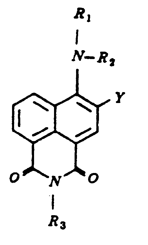

- Strukturierter Träger nach Anspruch 1, wobei das lichtstreuende Medium Titandioxid enthält.
- Strukturierter Träger nach Anspruch 1, wobei der Träger ein gehärtetes Epoxidharz enthält.
- Strukturierter Träger nach Anspruch 3, wobei der Farbstoff chemisch an den Träger gebunden ist.
- Strukturierter Träger nach Anspruch 4, wobei das lichtstreuende Medium Titandioxid enthält.
- Strukturierter Träger nach Anspruch 4, wobei das Metall Kupfer enthält.
- Strukturierter Träger nach Anspruch 1, wobei der mit (1) bezeichnete Farbstoff verwendet wird, wobei es sich bei R₁, R₂ und R₃ um Wasserstoff handelt und wobei der Farbstoff mit Bisphenol-A-Diglycidylether umgesetzt wird.
- Verfahren zur Erkennung von Fehlern in einem Träger nach Anspruch 1, das die folgenden Schritte umfaßt: Beleuchten des Trägers mit einer Quelle elektromagnetischer Strahlung, die sich dazu eignet, im Träger gestreut zu werden und Fluoreszenz im Farbstoff zu erzeugen; Erfassen der entstehenden Fluoreszenz aus dem Träger; sowie die weitere Verarbeitung des Trägers aufgrund dieser Erfassung.
- Verfahren nach Anspruch 7, wobei das lichtstreuende Medium Titandioxid enthält.
- Verfahren nach Anspruch 7, wobei der Träger ein gehärtetes Epoxidharz -enthält.
- Verfahren nach Anspruch 9, wobei der Farbstoff chemisch an den Träger gebunden ist.
- Verfahren nach Anspruch 10, wobei das lichtstreuende Medium Titandioxid enthält.
- Verfahren nach Anspruch 10, wobei das Metall Kupfer enthält.
- Verfahren nach Anspruch 7, wobei der mit (1) bezeichnete Farbstoff verwendet wird, wobei es sich bei R₁, R₂ und R₃ um Wasserstoff handelt und wobei der Farbstoff mit Bisphenol-A-Diglycidylether umgesetzt wird.
Applications Claiming Priority (2)
| Application Number | Priority Date | Filing Date | Title |
|---|---|---|---|
| US07/144,763 US4965208A (en) | 1983-07-29 | 1988-01-19 | Inspection of multipattern circuit boards |
| US144763 | 1988-01-19 |
Publications (2)
| Publication Number | Publication Date |
|---|---|
| EP0325355A1 EP0325355A1 (de) | 1989-07-26 |
| EP0325355B1 true EP0325355B1 (de) | 1995-06-21 |
Family
ID=22510025
Family Applications (1)
| Application Number | Title | Priority Date | Filing Date |
|---|---|---|---|
| EP19890300204 Expired - Lifetime EP0325355B1 (de) | 1988-01-19 | 1989-01-11 | Überprüfung von Leiterplatten mit Mehrfachmustern |
Country Status (7)
| Country | Link |
|---|---|
| US (1) | US4965208A (de) |
| EP (1) | EP0325355B1 (de) |
| JP (1) | JPH01198093A (de) |
| KR (1) | KR970006228B1 (de) |
| CA (1) | CA1335625C (de) |
| DE (1) | DE68923099T2 (de) |
| HK (1) | HK100496A (de) |
Families Citing this family (3)
| Publication number | Priority date | Publication date | Assignee | Title |
|---|---|---|---|---|
| TW203675B (de) * | 1991-08-28 | 1993-04-11 | Mitsubishi Gas Chemical Co | |
| EP1163389B2 (de) † | 1998-12-11 | 2009-12-16 | Isola USA Corp. | Sichtbares und fluoreszenzfarbstoff enthaltendes laminat |
| JP3695407B2 (ja) * | 2002-02-25 | 2005-09-14 | ソニーケミカル株式会社 | 硬化性接着剤組成物の硬化物の硬化レベルの非破壊検査方法及び電子装置の製造方法 |
Family Cites Families (4)
| Publication number | Priority date | Publication date | Assignee | Title |
|---|---|---|---|---|
| US3617744A (en) * | 1969-07-01 | 1971-11-02 | Bell Telephone Labor Inc | Method and apparatus for circuit module testing by comparison of a fluorescent image with a standard pattern |
| US4152723A (en) * | 1977-12-19 | 1979-05-01 | Sperry Rand Corporation | Method of inspecting circuit boards and apparatus therefor |
| CA1215615A (en) * | 1983-07-29 | 1986-12-23 | Edwin A. Chandross | Control of circuit board quality |
| US4774188A (en) * | 1983-07-29 | 1988-09-27 | American Telephone And Telegraph Company, At&T Bell Laboratories | Control of circuit board quality |
-
1988
- 1988-01-19 US US07/144,763 patent/US4965208A/en not_active Expired - Fee Related
- 1988-12-07 JP JP63307975A patent/JPH01198093A/ja active Granted
-
1989
- 1989-01-11 EP EP19890300204 patent/EP0325355B1/de not_active Expired - Lifetime
- 1989-01-11 DE DE68923099T patent/DE68923099T2/de not_active Expired - Fee Related
- 1989-01-13 KR KR89000290A patent/KR970006228B1/ko not_active Expired - Fee Related
- 1989-01-18 CA CA 588527 patent/CA1335625C/en not_active Expired - Fee Related
-
1996
- 1996-06-06 HK HK100496A patent/HK100496A/en not_active IP Right Cessation
Also Published As
| Publication number | Publication date |
|---|---|
| JPH0577354B2 (de) | 1993-10-26 |
| KR970006228B1 (en) | 1997-04-24 |
| US4965208A (en) | 1990-10-23 |
| JPH01198093A (ja) | 1989-08-09 |
| HK100496A (en) | 1996-06-14 |
| EP0325355A1 (de) | 1989-07-26 |
| CA1335625C (en) | 1995-05-23 |
| DE68923099T2 (de) | 1996-05-15 |
| DE68923099D1 (de) | 1995-07-27 |
Similar Documents
| Publication | Publication Date | Title |
|---|---|---|
| US4774188A (en) | Control of circuit board quality | |
| EP0438882A2 (de) | Verbesserte Fluoreszenzpolymere und daraus hergestellte Verbindungsstrukturen | |
| EP0325355B1 (de) | Überprüfung von Leiterplatten mit Mehrfachmustern | |
| KR100240373B1 (ko) | 인쇄 회로판용 기판 | |
| KR100225272B1 (ko) | 인쇄 회로판용 기판 | |
| EP0133351B1 (de) | Kontrolle der Qualität einer Schaltplatte | |
| EP0429027B1 (de) | Flammhemmende Klebstoffzusammensetzung und Laminate | |
| US5518656A (en) | Fluorescent detecting agents | |
| KR100218705B1 (ko) | 형광검출방식 자동 외관검사용 난연성 동박적층판용 수지조성물 | |
| EP1163389B1 (de) | Sichtbares und fluoreszenzfarbstoff enthaltendes laminat | |
| KR0182828B1 (ko) | 형광검출방식 자동외관검사용 난연성 동박적층판용 수지조성물 | |
| US20040009724A1 (en) | Method for identifying origin of and detecting defects in glass and quartz fiber products | |
| JPH0682384A (ja) | 金属箔張り積層板 | |
| JPH0294491A (ja) | 印刷配線板用銅張積層板 | |
| JPH05191000A (ja) | プリント配線用基板 | |
| JPH06112607A (ja) | 蛍光方式光学検査機対応回路基板 | |
| JPH032547A (ja) | 回路パターンの検査法 | |
| CN118222243A (zh) | 一种聚酰亚胺粘接剂、粘贴片、粘贴片材及其制备方法、荧光检测试剂盒 | |
| JPH1019882A (ja) | 接着剤付銅はくの評価方法 |
Legal Events
| Date | Code | Title | Description |
|---|---|---|---|
| PUAI | Public reference made under article 153(3) epc to a published international application that has entered the european phase |
Free format text: ORIGINAL CODE: 0009012 |
|
| AK | Designated contracting states |
Kind code of ref document: A1 Designated state(s): DE FR GB NL |
|
| 17P | Request for examination filed |
Effective date: 19900117 |
|
| 17Q | First examination report despatched |
Effective date: 19920311 |
|
| RAP3 | Party data changed (applicant data changed or rights of an application transferred) |
Owner name: AT&T CORP. |
|
| GRAA | (expected) grant |
Free format text: ORIGINAL CODE: 0009210 |
|
| AK | Designated contracting states |
Kind code of ref document: B1 Designated state(s): DE FR GB NL |
|
| ET | Fr: translation filed | ||
| REF | Corresponds to: |
Ref document number: 68923099 Country of ref document: DE Date of ref document: 19950727 |
|
| PLBE | No opposition filed within time limit |
Free format text: ORIGINAL CODE: 0009261 |
|
| STAA | Information on the status of an ep patent application or granted ep patent |
Free format text: STATUS: NO OPPOSITION FILED WITHIN TIME LIMIT |
|
| 26N | No opposition filed | ||
| PGFP | Annual fee paid to national office [announced via postgrant information from national office to epo] |
Ref country code: FR Payment date: 19991223 Year of fee payment: 12 |
|
| PGFP | Annual fee paid to national office [announced via postgrant information from national office to epo] |
Ref country code: NL Payment date: 19991227 Year of fee payment: 12 |
|
| PGFP | Annual fee paid to national office [announced via postgrant information from national office to epo] |
Ref country code: GB Payment date: 19991229 Year of fee payment: 12 |
|
| PGFP | Annual fee paid to national office [announced via postgrant information from national office to epo] |
Ref country code: DE Payment date: 20000331 Year of fee payment: 12 |
|
| PG25 | Lapsed in a contracting state [announced via postgrant information from national office to epo] |
Ref country code: GB Free format text: LAPSE BECAUSE OF NON-PAYMENT OF DUE FEES Effective date: 20010111 |
|
| PG25 | Lapsed in a contracting state [announced via postgrant information from national office to epo] |
Ref country code: NL Free format text: LAPSE BECAUSE OF NON-PAYMENT OF DUE FEES Effective date: 20010801 |
|
| GBPC | Gb: european patent ceased through non-payment of renewal fee |
Effective date: 20010111 |
|
| PG25 | Lapsed in a contracting state [announced via postgrant information from national office to epo] |
Ref country code: FR Free format text: LAPSE BECAUSE OF NON-PAYMENT OF DUE FEES Effective date: 20010928 |
|
| NLV4 | Nl: lapsed or anulled due to non-payment of the annual fee |
Effective date: 20010801 |
|
| PG25 | Lapsed in a contracting state [announced via postgrant information from national office to epo] |
Ref country code: DE Free format text: LAPSE BECAUSE OF NON-PAYMENT OF DUE FEES Effective date: 20011101 |
|
| REG | Reference to a national code |
Ref country code: FR Ref legal event code: ST |