EP0328329B1 - Flüssigkristall-Anzeigevorrichtung - Google Patents
Flüssigkristall-Anzeigevorrichtung Download PDFInfo
- Publication number
- EP0328329B1 EP0328329B1 EP89301134A EP89301134A EP0328329B1 EP 0328329 B1 EP0328329 B1 EP 0328329B1 EP 89301134 A EP89301134 A EP 89301134A EP 89301134 A EP89301134 A EP 89301134A EP 0328329 B1 EP0328329 B1 EP 0328329B1
- Authority
- EP
- European Patent Office
- Prior art keywords
- liquid crystal
- crystal display
- polarizer
- display device
- light
- Prior art date
- Legal status (The legal status is an assumption and is not a legal conclusion. Google has not performed a legal analysis and makes no representation as to the accuracy of the status listed.)
- Expired - Lifetime
Links
- 239000004973 liquid crystal related substance Substances 0.000 title claims description 88
- 239000010408 film Substances 0.000 claims description 44
- 239000000758 substrate Substances 0.000 claims description 42
- 230000010287 polarization Effects 0.000 claims description 25
- 239000002184 metal Substances 0.000 claims description 10
- 229910052751 metal Inorganic materials 0.000 claims description 10
- 239000010409 thin film Substances 0.000 claims description 4
- 239000001828 Gelatine Substances 0.000 claims description 3
- 229920000159 gelatin Polymers 0.000 claims description 3
- 235000019322 gelatine Nutrition 0.000 claims description 3
- 239000000049 pigment Substances 0.000 claims description 3
- 229910018487 Ni—Cr Inorganic materials 0.000 claims description 2
- 239000012212 insulator Substances 0.000 claims description 2
- 229920006254 polymer film Polymers 0.000 claims description 2
- 239000004065 semiconductor Substances 0.000 claims 3
- 239000011159 matrix material Substances 0.000 description 14
- 210000004027 cell Anatomy 0.000 description 8
- 238000000853 optical rotatory dispersion Methods 0.000 description 8
- BLRPTPMANUNPDV-UHFFFAOYSA-N Silane Chemical compound [SiH4] BLRPTPMANUNPDV-UHFFFAOYSA-N 0.000 description 6
- 229910021417 amorphous silicon Inorganic materials 0.000 description 6
- 230000015556 catabolic process Effects 0.000 description 6
- 239000003086 colorant Substances 0.000 description 6
- 238000006731 degradation reaction Methods 0.000 description 6
- 239000004988 Nematic liquid crystal Substances 0.000 description 5
- 239000011521 glass Substances 0.000 description 4
- 230000003287 optical effect Effects 0.000 description 4
- 238000002834 transmittance Methods 0.000 description 4
- 230000005540 biological transmission Effects 0.000 description 3
- 238000000034 method Methods 0.000 description 3
- 238000010276 construction Methods 0.000 description 2
- 210000002858 crystal cell Anatomy 0.000 description 2
- 238000004519 manufacturing process Methods 0.000 description 2
- 238000010586 diagram Methods 0.000 description 1
- 229910052736 halogen Inorganic materials 0.000 description 1
- 150000002367 halogens Chemical class 0.000 description 1
- 238000005286 illumination Methods 0.000 description 1
- 239000000463 material Substances 0.000 description 1
- 229910001507 metal halide Inorganic materials 0.000 description 1
- 150000005309 metal halides Chemical class 0.000 description 1
- 229920000642 polymer Polymers 0.000 description 1
- 229910052724 xenon Inorganic materials 0.000 description 1
- FHNFHKCVQCLJFQ-UHFFFAOYSA-N xenon atom Chemical compound [Xe] FHNFHKCVQCLJFQ-UHFFFAOYSA-N 0.000 description 1
Images
Classifications
-
- G—PHYSICS
- G02—OPTICS
- G02F—OPTICAL DEVICES OR ARRANGEMENTS FOR THE CONTROL OF LIGHT BY MODIFICATION OF THE OPTICAL PROPERTIES OF THE MEDIA OF THE ELEMENTS INVOLVED THEREIN; NON-LINEAR OPTICS; FREQUENCY-CHANGING OF LIGHT; OPTICAL LOGIC ELEMENTS; OPTICAL ANALOGUE/DIGITAL CONVERTERS
- G02F1/00—Devices or arrangements for the control of the intensity, colour, phase, polarisation or direction of light arriving from an independent light source, e.g. switching, gating or modulating; Non-linear optics
- G02F1/01—Devices or arrangements for the control of the intensity, colour, phase, polarisation or direction of light arriving from an independent light source, e.g. switching, gating or modulating; Non-linear optics for the control of the intensity, phase, polarisation or colour
- G02F1/13—Devices or arrangements for the control of the intensity, colour, phase, polarisation or direction of light arriving from an independent light source, e.g. switching, gating or modulating; Non-linear optics for the control of the intensity, phase, polarisation or colour based on liquid crystals, e.g. single liquid crystal display cells
- G02F1/133—Constructional arrangements; Operation of liquid crystal cells; Circuit arrangements
- G02F1/136—Liquid crystal cells structurally associated with a semi-conducting layer or substrate, e.g. cells forming part of an integrated circuit
- G02F1/1362—Active matrix addressed cells
-
- G—PHYSICS
- G02—OPTICS
- G02F—OPTICAL DEVICES OR ARRANGEMENTS FOR THE CONTROL OF LIGHT BY MODIFICATION OF THE OPTICAL PROPERTIES OF THE MEDIA OF THE ELEMENTS INVOLVED THEREIN; NON-LINEAR OPTICS; FREQUENCY-CHANGING OF LIGHT; OPTICAL LOGIC ELEMENTS; OPTICAL ANALOGUE/DIGITAL CONVERTERS
- G02F1/00—Devices or arrangements for the control of the intensity, colour, phase, polarisation or direction of light arriving from an independent light source, e.g. switching, gating or modulating; Non-linear optics
- G02F1/01—Devices or arrangements for the control of the intensity, colour, phase, polarisation or direction of light arriving from an independent light source, e.g. switching, gating or modulating; Non-linear optics for the control of the intensity, phase, polarisation or colour
- G02F1/13—Devices or arrangements for the control of the intensity, colour, phase, polarisation or direction of light arriving from an independent light source, e.g. switching, gating or modulating; Non-linear optics for the control of the intensity, phase, polarisation or colour based on liquid crystals, e.g. single liquid crystal display cells
- G02F1/133—Constructional arrangements; Operation of liquid crystal cells; Circuit arrangements
- G02F1/1333—Constructional arrangements; Manufacturing methods
- G02F1/1335—Structural association of cells with optical devices, e.g. polarisers or reflectors
- G02F1/133509—Filters, e.g. light shielding masks
- G02F1/133512—Light shielding layers, e.g. black matrix
Definitions
- the present invention relates to a projection type liquid crystal display device, and more particularly, to such a device of active matrix type.
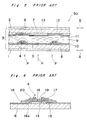
- Fig. 5 is a schematic longitudinal cross-sectional view showing the main portion of a conventional active matrix type liquid crystal display device 50.
- a liquid crystal display cell 3 is arranged between two polarizers 1 and 2 arranged so that the axes of polarization thereof are parallel to each other.
- the liquid crystal display cell 3 is composed of a transparent insulating substrate 6 of glass on which thin film transistors (TFTs) 4 and transparent conductive picture element electrodes 5 for displaying picture elements are formed, another transparent insulating substrate 8 of glass on which transparent conductive electrodes 7 are formed so as to oppose the electrodes 5 of the former substrate 6, and a liquid crystal layer 9 arranged between the transparent substrates 6 and 8.
- TFTs 4 are formed in a matrix so as to correspond to the respective picture element electrodes 5.
- An orientation film 10 is formed on the inner surface of the transparent substrate 6 so as to cover the TFTs 4 and the picture element electrodes 5, and an orientation film 11 is formed on the inner surface of the transparent substrate 8 so as to cover the electrodes 7.
- Nematic liquid crystal molecules contained in the liquid crystal layer 9 are twisted by 90° between the orientation films 10 and 11 while zero voltage is applied between the electrodes 5 and 7. Namely, the nematic liquid crystal molecules in the layer 9 are set in the twisted nematic mode.
- Shading films 12 are formed between each of the electrodes 7 and the substrate 8 so as to face the respective TFTs 4, and colour filter layers 13 are also formed on the inner surfaces of the substrate 8 so as to face the respective portions of the picture element electrodes 5 where the TFTs 4 are not formed.
- arrows A and B represent the directions of the polarization axes of the polarizer 1 and the polarizer 2, respectively.
- Fig. 6 is an enlarged schematic longitudinal cross-sectional view showing the TFT 4 used as a switching element for driving the liquid crystal layer 9 in the liquid crystal display device 50.
- a gate electrode 14 of a metal film is formed on the surface of the transparent substrate 6, and a gate insulating film 15 is formed thereon. Furthermore, an amorphous silicon hydride film 16 functioning as an active layer is formed on the film 15, and n+ amorphous silicon hydride films 17 and 18 are formed thereon.
- a numeral 19 denotes an insulating film, and a numeral 20 denotes a metal film.
- liquid crystal display device 50 constructed as described above, light is emitted from a light source (not shown) arranged on the side of the outer surface of the polarizer 1 as indicated by arrows P, and the emitted light is converted to a linearly polarized light by the polarizer 1.
- the linearly polarized light is transmitted through the transparent substrate 6, the electrode 5, the liquid crystal layer 9, the electrode 7, the colour filter layer 13 and the transparent substrate 8, sequentially, and is incident to the polarizer 2.
- the liquid crystal layer 9 is set in the twisted nematic mode and the respective polarization axes of the polarizers 1 and 2 are in parallel to each other, when zero voltage is applied between the electrodes 5 and 7, the polarization axis of the light transmitted through the polarizer 1 from the light source is twisted by 90° according to the rotary polarization characteristic of the liquid crystal layer 9, and therefore, the polarization axis thereof becomes orthogonal to that of the polarizer 2, resulting in that the light is prevented from being transmitted through the polarizer 2.
- the rotatory polarization characteristic of the liquid crystal layer 9 is dissolved when a predetermined voltage is applied between the electrodes 5 and 7, the polarization axis of the light incident to the polarizer 2 is coincident with that of the polarizer 2, resulting in that the light is transmitted through the polarizer 2.
- the voltage to be applied between the electrodes 5 and 7 is controlled by the TFTs 4.
- the picture elements corresponding to the electrodes 5 and 7 between which the predetermined voltage is applied according to the above operation acquire a transparent state, and a coloured display is effected by the transmitted light coloured by the colour filter layer 13.
- the light transmitted through the polarizer 1 and the transparent substrate 6 is incident to the TFTs 4 comprising the amorphous silicon hydride film 16 having a high photoconductivity for visible light.
- the gate electrode 14 of metal film functions as a shading film, the increase of the OFF current in the TFTs 4 caused by the photoconductivity of the film 16 is prevented.
- images etc. are projected on a screen through a projecting lens in a magnification mode with use of the active matrix type liquid crystal display device using the TFTs 4 having the aforementioned amorphous silicon hydride film 16 as switching elements, an extremely strong light is required as the light source in order to produce a bright display.
- the illuminance of the light incident to the liquid crystal display device 50 is in a range of several hundred thousand to several million lx.
- the gate electrode 14 of the TFT 4 also functions as the shading film, the increase of the OFF current in the TFT 4 caused by the photoconductivity is prevented, resulting in that the degradation of the display characteristics can be avoided.
- the display mode is used in which the light is not transmitted at the time of the application of zero voltage and the light is transmitted by dissolving the rotatory polarization characteristic of the liquid crystal layer 9 when a predetermined voltage is applied.
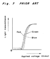
- the display device because the optical rotatory dispersion is caused in the liquid crystal layer 9, there is a problem that the different electro-optical characteristics are obtained respectively for light having different wavelengths such as red, green and blue.
- Fig. 7 shows the dependency of the transmittance on the root mean square value of the applied voltage with a parameter of the wavelength of light (red, green and blue) in the aforementioned active matrix type liquid crystal display device 50.
- the vertical axis is the light transmittance and the horizontal axis is the root mean square value of the applied voltage.
- the threshold voltage of the TFT 4 is shifted with lapse of the light projecting time, resulting in the degradation of the display characteristic.
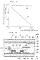
- Fig. 3 shows the relationship between the light projecting time (hours) and the shift amount ⁇ V TH (volts) of the threshold voltage of the TFT 4, wherein the visible light having an illuminance of 700,000 lx is projected onto the TFT 4.
- the curve l1 shows the shift amount ⁇ V TH of the threshold voltage of the TFT 4 in the conventional active matrix type liquid crystal display device 50.
- the threshold voltage of the TFT 4 is shifted gradually.
- the colour reproductivities for red, green and blue colours are equalized by setting respective gaps d of the portions of the liquid crystal cell corresponding to individual picture elements for displaying the red, green and blue colours so as to make the ratio ⁇ n ⁇ d/ ⁇ constant, wherein ⁇ n is the birefringence of the liquid crystal and ⁇ is the wavelength of light.
- An essential object of the present invention is to provide a projection type liquid crystal display device having excellent colour display characteristics without causing changes in colours to be displayed and degradation of the display which may be caused by the light projection for a long time.
- This invention provides a projection type liquid crystal display device comprising: a first polarizer; a second polarizer; a liquid crystal display cell arranged between said first and second polarizers for displaying an image thereon, said liquid crystal display cell including a liquid crystal layer arranged between mutually parallel first and second transparent insulating substrates; first transparent electrodes formed on an inner surface of said first transparent insulating substrate; second transparent electrodes formed on an inner surface of said second transparent insulating substrate so as to oppose said first transparent electrodes; switching means, arranged on an inner surface of said first transparent insulating substrate, for controlling an applied voltage between said first and second transparent electrodes so as to drive picture elements defined between said first and second transparent electrodes; a light source, arranged on the side of an outer surface of said second polarizer, for emitting light through said second polarizer, said second transparent insulating substrate, said liquid crystal layer, said first transparent insulating substrate and said first polarizer toward a display screen arranged on the side of an outer surface of said first polarizer; and shading
- the light emitted from the light source is transmitted through the first polarizer in the twisted nematic mode, and, when the twisted nematic mode is dissolved by applying a predetermined voltage between the first and second electrodes, the emitted light is prevented from being transmitted through the first polarizer. Therefore, possible changes in the colours due to the optical rotatory dispersion is never caused on the display screen and the colour reproductivity can be improved.
- the shading means are preferably arranged so as to also shade a rim portion of the first transparent electrode. Then, since the light incident to the switching means and the rim portion of the first transparent electrode from the light source through the second polarizer is shaded certainly by the shading means, the degradation of the display characteristic of the switching means can be prevented and the display with a high contrast can be obtained.
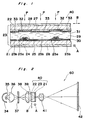
- Fig. 1 is a schematic longitudinal cross-sectional view showing the main portion of an active matrix type liquid crystal display device 40 of the first preferred embodiment according to the present invention.
- a liquid crystal display cell 23 is arranged between the first and second polarizers 21 and 22 arranged so that the polarization axes thereof are orthogonal to each other.
- the liquid crystal display cell 23 is composed of the first transparent insulating substrate 26 of glass on which TFTs 24 functioning as a switching element for driving a liquid crystal layer 29 and transparent conductive picture element electrodes 25 for displaying picture elements are formed, the second transparent insulating substrate 28 of glass on which transparent conductive electrodes 27 are formed so as to oppose the electrodes 25 of the first substrate 26, and the liquid crystal layer 29 arranged between the transparent substrates 26 and 28.
- the picture element electrodes 25 cross the electrodes 27, respectively, in a known manner.
- the structure of the TFT 24 is the same as that of the conventional TFT 4 shown in Fig. 6, therefore, the description thereof is omitted.
- the TFTs 24 are formed in a matrix so as to correspond to the respective electrodes 25.
- An orientation film 30 is formed on the inner surface of the transparent substrate 26 so as to cover the TFTs 24 and the picture element electrodes 25, and an orientation film 31 is formed on the inner surface of the transparent substrate 28 so as to cover the electrodes 27.
- Nematic liquid crystal molecules contained in the liquid crystal layer 29 are twisted by 90° between the orientation films 30 and 31 while zero voltage is applied to the liquid crystal layer 29.
- the nematic liquid crystal molecules in the layer 29 are set in the twisted nematic mode, so that the polarization axis of the light incident to the first polarizer 21 after transmission through the liquid crystal layer 29 becomes parallel to that of the first polarizer 21 and the polarization axis of the light incident to the second polarizer 22 after transmission through the liquid crystal layer 29 becomes parallel to that of the second polarizer 22.
- Shading films 32 are formed between each of the electrodes 27 and the substrate 28 so as to face the whole area of the respective TFTs 24 and the rim portions 25a of the electrodes 25.
- Colour filter layers 33 are also formed on the inner surface of the substrate 28 so as to face the other respective main portions 25b of the picture element electrodes 25 than the rim portions 25a thereof. Since the aforementioned shading films 32 are formed so as to correspond to the respective TFTs 24 and the respective electrodes 25, the shading films 32 have a lattice shape.
- the shading films 32 are preferably made of metal such as Cr, Ni, Al and Ni-Cr. Alternatively, the shading films 32 may be made of a gelatine film or an organic high polymer coloured with a dye or a pigment.
- an arrow A having a perpendicular direction to the surface of the paper represents a direction of the polarization axis of the first polarizer 21
- arrows B represent a direction of the polarization axis of the second polarizer 22.
- Fig. 2 is a schematic view showing a projecting type display optical system 60 comprising the aforementioned liquid crystal display device 40.
- a mirror 34, a light source 35, the first condenser lens 36, a filter 37 for cutting heat rays, the second condenser lens 38, a filter 39 for cutting ultraviolet rays, the liquid crystal display device 40, a projecting lens 41 and a screen 42 are arranged sequentially.
- the liquid crystal display device 40 is arranged so that the second polarizer 22 thereof is directed to the light source 35.
- the light source 35 is preferably a halogen lamp, a xenon lamp, or a metal halide lamp in order to produce a bright display.
- the light emitted from the light source 35 is condensed by the mirror 34 and the first condenser lens 36.
- the condensed light is transmitted through the filter 37 for cutting heat rays, and the transmitted light is incident to the second condenser lens 38.
- the light transmitted through the second condenser lens 38 is transmitted through the filter 39 for cutting ultraviolet rays and is incident to the second polarizer 22 of the liquid crystal display device 40. The light thereof is shown by an arrow P in Fig. 1.
- the light incident to the second polarizer 22 becomes a linearly polarized light, and light thereof is transmitted through the second transparent substrate 28, the colour filter layer 33, the electrode 27, the liquid crystal layer 29, the electrode 25 and the first transparent substrate 26, sequentially, and thereafter, the transmitted light is incident to the first polarizer 21.
- the liquid crystal layer 29 is set in the twisted nematic mode in which the liquid crystal molecules contained in the layer 29 are twisted by 90° and the first and second polarizers 21 and 22 are arranged so that the polarization axes thereof are orthogonal to each other. Therefore, at the time of the application of zero voltage between the electrodes 25 and 27, the polarization axis of the light transmitted through the second polarizer 22 after emission from the light source 35 is twisted by 90° according to the rotatory polarization characteristic of the liquid crystal layer 29 and is parallel to the polarization axis of the first polarizer 21, resulting in that the light is allowed to be transmitted through the first polarizer 21.
- the rotatory polarization characteristic of the liquid crystal layer 29 is dissolved and the polarization axis of the light incident to the first polarizer 21 is orthogonal to that of the first polarizer 21, resulting in that the light is prevented from being transmittted through the first polarizer 21.
- the light transmittance of the respective picture elements is changed, and then, the transmitted light coloured by the colour filter layer 33 is transmitted through the projecting lens 41, and the enlarged image is formed on the screen 42 with a coloured display.
- the liquid crystal layer 29 is set in the twisted nematic mode and the phenomenon of the optical rotatory dispersion appears in the layer 29.
- the twist of the polarization axis of the liquid crystal layer 29 is almost dissolved. Therefore, the phenomenon of the optical rotatory dispersion almost does not appear in the layer 29, resulting in that the leak light due to the optical rotatory dispersion is not caused.
- the display with use of the liquid crystal display device 40 has an extremely fine colour reproductivity.
- the shading film 32 formed on the second transparent substrate 28 prevents the light from the light source 35 from being incident to the TFT 24, the shift of the threshold voltage of the TFT 24 due to the light projection for a relatively long time is prevented.
- the curve l2 of Fig. 3 shows the relationship between the light projecting time (hours) of the visible light having an illuminance of 700,000 lx incident to the TFT 24 in the liquid crystal display device 40 and the shift amount ⁇ V TH (volts) of the threshold voltage of the TFT 24.
- the threshold voltage of the TFT 24 is almost not shifted. Therefore, degradation of the display characteristic can be prevented. Even when a predetermined voltage is applied to the layer 29, the applied voltage does not influence the shading film 32, and the shading film 32 is also used for shading the light transmitted through the rim portions 25a of the electrodes 25 which cannot shade the light, resulting in that the display with a high contrast can be obtained.
- the colour filter layer 33 is used as a means for separating colours.
- a dichroic mirror or a dichroic prism may be used as the means for separating colours.
- the arrangement of the colour filter layer 33 is not limited to the case where the colour filter layer 33 is arranged between the second and first polarizers 22 and 21.
- Fig. 4 is a schematic longitudinal cross-sectional view showing the main portion of an active matrix type liquid crystal display device 40a of the second preferred embodiment according to the present invention.
- the liquid crystal display device of the second preferred embodiment comprises a non-linear type element used as the switching element for driving the liquid crystal layer 29.
- the other construction thereof is the same as that of the liquid crystal display device 40 of the first preferred embodiment. Therefore, in Fig. 4, the same components as the components of the liquid crystal display device 40 of the first preferred embodiment are denoted respectively by the same numerals as those of the components of the liquid crystal display device 40 of the first preferred embodiment, and the descriptions thereof are omitted.
- a ring diode is used as the non-linear element 43, wherein the ring diode is composed of two diodes 44 and 45 connected in parallel so that the forward direction of one diode is parallel to the backward direction of another diode, and the diodes 44 and 45 have an amorphous silicon hydride film of the PIN junction type as an active layer.
- the shading film 32 for shading the light transmission through the whole area of the non-linear type element 43 and the rim portion 25a of the electrode 25 must be an insulating film.
- the shading film 32 is preferably a gelatine film or a high polymer film coloured with a dye or a pigment.
- the diode 44 is composed of an n-layer 44a, an i-layer 44b and a p-layer 44c
- the diode 45 is composed of an n-layer 45a, an i-layer 45b and a p-layer 45c.
- the numerals 46 and 47 denote metal films
- the numeral 48 denotes an insulating film.
- an arrow A having a perpendicular direction to the surface of the paper represents a direction of the polarization axis of the first polarizer 21
- arrows B represent a direction of the polarization axis of the second polarizer 32.
- the non-linear type element 43 may be the aforementioned two diodes 44 and 45 connected in series to each other in a forward direction or a backward direction thereof.
- the non-linear type element 43 may also be a Schottky junction element, or a so-called Metal Insulator Metal element.
Landscapes
- Physics & Mathematics (AREA)
- Nonlinear Science (AREA)
- Mathematical Physics (AREA)
- Chemical & Material Sciences (AREA)
- Crystallography & Structural Chemistry (AREA)
- General Physics & Mathematics (AREA)
- Optics & Photonics (AREA)
- Engineering & Computer Science (AREA)
- Microelectronics & Electronic Packaging (AREA)
- Liquid Crystal (AREA)
- Devices For Indicating Variable Information By Combining Individual Elements (AREA)
Claims (8)
- Flüssigkristall-Projektionsanzeigevorrichtung mit:- einem ersten Polarisator (21);- einem zweiten Polarisator (22);- einer Flüssigkristall-Anzeigezelle (23), die zwischen dem ersten und zweiten Polarisator angeordnet ist, um auf ihr ein Bild darzustellen, wobei die Flüssigkristall-Anzeigezelle eine Flüssigkristallschicht (29) aufweist, die zwischen einem ersten (26) und einem zweiten (28) transparenten, isolierenden Substrat angeordnet ist, die zueinander parallel sind;- ersten transparenten Elektroden (25), die auf der Innenfläche des ersten transparenten, isolierenden Substrats angeordnet sind;- zweiten transparenten Elektroden (27), die auf der Innenfläche des zweiten transparenten, isolierenden Substrats so angeordnet sind, daß sie den ersten transparenten Elektroden gegenüberstehen;- einer Schalteinrichtung (24; 43), die auf der Innenfläche des ersten transparenten, isolierenden Substrats angeordnet ist, um eine zwischen die erste und zweite transparente Elektrode angelegte Spannung so einzustellen, daß Bildelemente gesteuert werden, die zwischen den ersten und zweiten transparenten Elektroden festgelegt sind;- einer Lichtquelle (35), die auf der Seite der Außenfläche des zweiten Polarisators (22) angeordnet ist, um Licht durch den zweiten Polarisator, das zweite transparente, isolierende Substrat (28), die Flüssigkristallschicht (29), das erste transparente, isolierende Substrat (26) und den ersten Polarisator (21) zu einem Anzeigeschirm (42) hin zu emittieren, der auf der Seite der Außenfläche des ersten Polarisators (21) angeordnet ist; und- einer Ausblendeinrichtung (32), die auf dem zweiten transparenten, isolierenden Substrat (28) so angeordnet ist, daß sie das emittierte Licht ausblendet, das zumindest auf die Schalteinrichtung (24; 43) fallen würde;- wobei die jeweiligen Polarisationsachsen des ersten und zweiten Polarisators so eingestellt sind, daß verhindert wird, daß das von der Lichtquelle emittierte Licht durch den zweiten Polarisator, die Flüssigkristall-Anzeigezelle und den ersten Polarisator hindurchgestrahlt wird, wenn eine vorgegebene Spannung an die erste und zweite transparente Elektrode angelegt ist, und das Licht von derselben dort hindurchgestrahlt werden kann, wenn die Spannung Null angelegt wird.
- Flüssigkristall-Projektionsanzeigevorrichtung nach Anspruch 1, bei der die Ausblendeinrichtung (32) so ausgebildet ist, daß sie auch einen Randbereich (25a) der ersten transparenten Elektroden (25) ausblendet.
- Flüssigkristall-Projektionsanzeigevorrichtung nach Anspruch 2, bei der die Schalteinrichtung einen Dünnfilmtransistor (24) enthält.
- Flüssigkristall-Projektionsanzeigevorrichtung nach Anspruch 3, bei der der Filmtransistor (24) eine Gateelektrode (14), die auf der Innenfläche des ersten transparenten, isolierenden Substrats ausgebildet ist, einen auf der Gateelektrode ausgebildeten elektrisch isolierenden Film (15), einen auf dem elektrisch isolierenden Film ausgebildeten Halbleiterfilm (16) und eine Sourceelektrode sowie eine Drainelektrode, die auf dem Halbleiterfilm ausgebildet sind, aufweist, wobei die Breite des Halbleiterfilms (16) größer als die Breite der Gateelektrode (14) ist.
- Flüssigkristall-Projektionsanzeigevorrichtung nach Anspruch 2, bei der die Schalteinrichtung ein nichtlineares Element (43) aufweist.
- Flüssigkristall-Projektionsanzeigevorrichtung nach Anspruch 5, bei der das nichtlineare Element zwei parallel oder in Reihe geschaltete Dioden (44, 45) oder ein Element mit Schottky-Übergang oder ein Metall-Isolator-Metall-Element ist.
- Flüssigkristall-Projektionsanzeigevorrichtung nach einem der Ansprüche 2 bis 6, bei dem die Ausblendeinrichtung (32) aus einem Metallfilm aus Cr, Ni, Al oder Ni-Cr besteht.
- Flüssigkristall-Projektionsanzeigevorrichtung nach einem der Ansprüche 2 bis 6, bei der die Ausblendeinrichtung (32) aus einem Gelatinefilm oder einem Film aus einem organischen Hochpolymer besteht, eingefärbt mit einem Farbstoff oder einem Pigment.
Applications Claiming Priority (2)
| Application Number | Priority Date | Filing Date | Title |
|---|---|---|---|
| JP26171/88 | 1988-02-06 | ||
| JP63026171A JPH01201622A (ja) | 1988-02-06 | 1988-02-06 | 投映型表示装置 |
Publications (3)
| Publication Number | Publication Date |
|---|---|
| EP0328329A2 EP0328329A2 (de) | 1989-08-16 |
| EP0328329A3 EP0328329A3 (de) | 1991-01-16 |
| EP0328329B1 true EP0328329B1 (de) | 1995-04-26 |
Family
ID=12186090
Family Applications (1)
| Application Number | Title | Priority Date | Filing Date |
|---|---|---|---|
| EP89301134A Expired - Lifetime EP0328329B1 (de) | 1988-02-06 | 1989-02-06 | Flüssigkristall-Anzeigevorrichtung |
Country Status (4)
| Country | Link |
|---|---|
| US (1) | US5073772A (de) |
| EP (1) | EP0328329B1 (de) |
| JP (1) | JPH01201622A (de) |
| DE (1) | DE68922322T2 (de) |
Families Citing this family (25)
| Publication number | Priority date | Publication date | Assignee | Title |
|---|---|---|---|---|
| US5420708A (en) * | 1990-08-31 | 1995-05-30 | Idemitsu Kosan Co., Ltd. | Color filters, including taking out electrodes or post-ito layer |
| US5206749A (en) | 1990-12-31 | 1993-04-27 | Kopin Corporation | Liquid crystal display having essentially single crystal transistors pixels and driving circuits |
| US5666175A (en) * | 1990-12-31 | 1997-09-09 | Kopin Corporation | Optical systems for displays |
| US5475514A (en) * | 1990-12-31 | 1995-12-12 | Kopin Corporation | Transferred single crystal arrayed devices including a light shield for projection displays |
| US5362671A (en) * | 1990-12-31 | 1994-11-08 | Kopin Corporation | Method of fabricating single crystal silicon arrayed devices for display panels |
| US5317436A (en) * | 1990-12-31 | 1994-05-31 | Kopin Corporation | A slide assembly for projector with active matrix moveably mounted to housing |
| US5396304A (en) * | 1990-12-31 | 1995-03-07 | Kopin Corporation | Slide projector mountable light valve display |
| US5528397A (en) | 1991-12-03 | 1996-06-18 | Kopin Corporation | Single crystal silicon transistors for display panels |
| JPH04240826A (ja) * | 1991-01-25 | 1992-08-28 | Nec Corp | 透過型液晶表示装置 |
| JP2794499B2 (ja) | 1991-03-26 | 1998-09-03 | 株式会社半導体エネルギー研究所 | 半導体装置の作製方法 |
| JP2905619B2 (ja) * | 1991-05-23 | 1999-06-14 | シャープ株式会社 | アクティブマトリクス型液晶表示素子 |
| FR2682493B1 (fr) * | 1991-10-11 | 1994-02-04 | Thomson Lcd | Dispositif d'amelioration du contraste d'un ecran a cristal liquide et son procede de fabrication. |
| US5467154A (en) * | 1992-02-20 | 1995-11-14 | Kopin Corporation | Projection monitor |
| US5692820A (en) * | 1992-02-20 | 1997-12-02 | Kopin Corporation | Projection monitor |
| US5398127A (en) * | 1992-03-03 | 1995-03-14 | Matsushita Electric Industrial Co., Ltd. | Active matrix twisted nematic liquid crystal display with rubbing direction 1-44 degrees to the electrodes |
| US6608654B2 (en) | 1992-09-11 | 2003-08-19 | Kopin Corporation | Methods of fabricating active matrix pixel electrodes |
| US5705424A (en) * | 1992-09-11 | 1998-01-06 | Kopin Corporation | Process of fabricating active matrix pixel electrodes |
| US5673127A (en) | 1993-12-01 | 1997-09-30 | Matsushita Electric Industrial Co., Ltd. | Display panel and display device using a display panel |
| US5664859A (en) * | 1994-01-03 | 1997-09-09 | Kopin Corporation | Projection display docking system |
| FR2721427B1 (fr) * | 1994-06-17 | 1996-08-14 | Bruno Vinouze | Ecran d'affichage à cristaux liquides à grille diffusante. |
| JP2827920B2 (ja) * | 1994-10-13 | 1998-11-25 | 松下電器産業株式会社 | カラー液晶表示パネル |
| US6778229B2 (en) * | 2001-10-02 | 2004-08-17 | Fujitsu Display Technologies Corporation | Liquid crystal display device and method of fabricating the same |
| JP4197404B2 (ja) | 2001-10-02 | 2008-12-17 | シャープ株式会社 | 液晶表示装置およびその製造方法 |
| WO2006005968A1 (en) | 2004-07-14 | 2006-01-19 | House-Building Society #887 'paupio Murai' | Method and device for regulation and control of transparence and translucence of glazing or oilcloth |
| CN109828015B (zh) * | 2019-03-07 | 2021-07-06 | 江苏友润微电子有限公司 | 基于有机晶体管氨气传感器芯片及其制备方法 |
Family Cites Families (12)
| Publication number | Priority date | Publication date | Assignee | Title |
|---|---|---|---|---|
| CH564206A5 (de) * | 1973-09-27 | 1975-07-15 | Bbc Brown Boveri & Cie | |
| FR2466071A1 (fr) * | 1979-09-21 | 1981-03-27 | Thomson Csf | Dispositif de projection d'images en couleurs sur un ecran, et systeme de visualisation comprenant un tel dispositif |
| JPS5961818A (ja) * | 1982-10-01 | 1984-04-09 | Seiko Epson Corp | 液晶表示装置 |
| JPS59137930A (ja) * | 1983-01-28 | 1984-08-08 | Fuji Photo Film Co Ltd | カラ−光プリンタヘツド |
| JPS6043631A (ja) * | 1983-08-20 | 1985-03-08 | Canon Inc | 表示パネル |
| FR2551902B1 (fr) * | 1983-09-13 | 1986-01-24 | Thomson Csf | Ecran de visualisation a adressage par elements non lineaires et son procede de fabrication |
| US4632514A (en) * | 1984-01-31 | 1986-12-30 | Matsushita Electric Industrial Co., Ltd. | Color liquid crystal display apparatus |
| JPS60222821A (ja) * | 1984-04-20 | 1985-11-07 | Canon Inc | カラ−液晶表示セル |
| JPS60172131U (ja) * | 1984-04-20 | 1985-11-14 | ホシデン株式会社 | カラ−液晶表示器 |
| JPH0750381B2 (ja) * | 1984-12-20 | 1995-05-31 | キヤノン株式会社 | カラー液晶表示装置 |
| JPS6280626A (ja) * | 1985-10-04 | 1987-04-14 | Hosiden Electronics Co Ltd | 液晶表示素子 |
| JPS62299940A (ja) * | 1986-06-20 | 1987-12-26 | Seiko Epson Corp | 液晶ライトバルブ |
-
1988
- 1988-02-06 JP JP63026171A patent/JPH01201622A/ja active Pending
-
1989
- 1989-02-03 US US07/305,779 patent/US5073772A/en not_active Expired - Lifetime
- 1989-02-06 EP EP89301134A patent/EP0328329B1/de not_active Expired - Lifetime
- 1989-02-06 DE DE68922322T patent/DE68922322T2/de not_active Expired - Lifetime
Also Published As
| Publication number | Publication date |
|---|---|
| EP0328329A3 (de) | 1991-01-16 |
| DE68922322T2 (de) | 1996-01-04 |
| DE68922322D1 (de) | 1995-06-01 |
| EP0328329A2 (de) | 1989-08-16 |
| JPH01201622A (ja) | 1989-08-14 |
| US5073772A (en) | 1991-12-17 |
Similar Documents
| Publication | Publication Date | Title |
|---|---|---|
| US5073772A (en) | Liquid crystal display device | |
| EP0377757B1 (de) | Reflektive elektrooptische flüssigkristallvorrichtung und projektionsanzeigevorrichtung unter verwendung derselben | |
| KR100258048B1 (ko) | 직렬 연결된 엘씨 필터를 구비한 칼라 표시 장치 | |
| JP3779052B2 (ja) | 液晶プロジェクタ | |
| US4995702A (en) | Projection-type display device | |
| US5157523A (en) | Projection type liquid crystal display unit including orthogonal phase plates | |
| US5477359A (en) | Liquid crystal projector having a vertical orientating polyimide film | |
| KR100189278B1 (ko) | 투영형 칼라 표시 장치 | |
| EP0522620A2 (de) | Bildwiedergabenanordnung | |
| US5384649A (en) | Liquid crystal spatial light modulator with electrically isolated reflecting films connected to electrically isolated pixel portions of photo conductor | |
| US5037196A (en) | Projection-type color display apparatus | |
| JPH0743707A (ja) | 液晶表示装置及びその製造方法 | |
| KR100348359B1 (ko) | 액정표시장치 | |
| US20060290851A1 (en) | Display apparatus having innovative array substrate | |
| US11281043B2 (en) | Display panel and display apparatus | |
| Uchida | Multicolored liquid crystal displays | |
| JP2742788B2 (ja) | 投射型表示装置 | |
| JPH021816A (ja) | 投影型表示装置 | |
| JP2000056297A (ja) | 液晶表示デバイス | |
| JPH05346566A (ja) | 投影型カラー画像表示装置 | |
| JPS6364031A (ja) | マトリクス表示装置 | |
| JPH11101991A (ja) | 液晶表示素子及びこれを用いた投射型表示装置 | |
| KR920006145Y1 (ko) | 컬러액정 표시장치 | |
| JPH1195212A (ja) | 反射型液晶表示素子および液晶プロジェクタ | |
| JP2798074B2 (ja) | 投射型表示装置 |
Legal Events
| Date | Code | Title | Description |
|---|---|---|---|
| PUAI | Public reference made under article 153(3) epc to a published international application that has entered the european phase |
Free format text: ORIGINAL CODE: 0009012 |
|
| AK | Designated contracting states |
Kind code of ref document: A2 Designated state(s): DE FR GB |
|
| PUAL | Search report despatched |
Free format text: ORIGINAL CODE: 0009013 |
|
| AK | Designated contracting states |
Kind code of ref document: A3 Designated state(s): DE FR GB |
|
| 17P | Request for examination filed |
Effective date: 19901214 |
|
| 17Q | First examination report despatched |
Effective date: 19921111 |
|
| GRAA | (expected) grant |
Free format text: ORIGINAL CODE: 0009210 |
|
| AK | Designated contracting states |
Kind code of ref document: B1 Designated state(s): DE FR GB |
|
| REF | Corresponds to: |
Ref document number: 68922322 Country of ref document: DE Date of ref document: 19950601 |
|
| ET | Fr: translation filed | ||
| PLBE | No opposition filed within time limit |
Free format text: ORIGINAL CODE: 0009261 |
|
| STAA | Information on the status of an ep patent application or granted ep patent |
Free format text: STATUS: NO OPPOSITION FILED WITHIN TIME LIMIT |
|
| 26N | No opposition filed | ||
| REG | Reference to a national code |
Ref country code: GB Ref legal event code: IF02 |
|
| PGFP | Annual fee paid to national office [announced via postgrant information from national office to epo] |
Ref country code: DE Payment date: 20080131 Year of fee payment: 20 Ref country code: GB Payment date: 20080206 Year of fee payment: 20 |
|
| PGFP | Annual fee paid to national office [announced via postgrant information from national office to epo] |
Ref country code: FR Payment date: 20080208 Year of fee payment: 20 |
|
| REG | Reference to a national code |
Ref country code: GB Ref legal event code: PE20 Expiry date: 20090205 |
|
| PG25 | Lapsed in a contracting state [announced via postgrant information from national office to epo] |
Ref country code: GB Free format text: LAPSE BECAUSE OF EXPIRATION OF PROTECTION Effective date: 20090205 |