EP0329247B1 - Circuit de tension de référence à bande interdite - Google Patents
Circuit de tension de référence à bande interdite Download PDFInfo
- Publication number
- EP0329247B1 EP0329247B1 EP89200344A EP89200344A EP0329247B1 EP 0329247 B1 EP0329247 B1 EP 0329247B1 EP 89200344 A EP89200344 A EP 89200344A EP 89200344 A EP89200344 A EP 89200344A EP 0329247 B1 EP0329247 B1 EP 0329247B1
- Authority
- EP
- European Patent Office
- Prior art keywords
- arrangement
- voltage
- transistor
- transistors
- differential amplifier
- Prior art date
- Legal status (The legal status is an assumption and is not a legal conclusion. Google has not performed a legal analysis and makes no representation as to the accuracy of the status listed.)
- Expired - Lifetime
Links
- 230000000694 effects Effects 0.000 description 7
- 238000003491 array Methods 0.000 description 6
- 230000002411 adverse Effects 0.000 description 2
- 238000010276 construction Methods 0.000 description 1
- 230000007423 decrease Effects 0.000 description 1
- 238000005516 engineering process Methods 0.000 description 1
- 230000002349 favourable effect Effects 0.000 description 1
- 230000010354 integration Effects 0.000 description 1
- 239000007787 solid Substances 0.000 description 1
Images
Classifications
-
- G—PHYSICS
- G05—CONTROLLING; REGULATING
- G05F—SYSTEMS FOR REGULATING ELECTRIC OR MAGNETIC VARIABLES
- G05F3/00—Non-retroactive systems for regulating electric variables by using an uncontrolled element, or an uncontrolled combination of elements, such element or such combination having self-regulating properties
- G05F3/02—Regulating voltage or current
- G05F3/08—Regulating voltage or current wherein the variable is DC
- G05F3/10—Regulating voltage or current wherein the variable is DC using uncontrolled devices with non-linear characteristics
- G05F3/16—Regulating voltage or current wherein the variable is DC using uncontrolled devices with non-linear characteristics being semiconductor devices
- G05F3/20—Regulating voltage or current wherein the variable is DC using uncontrolled devices with non-linear characteristics being semiconductor devices using diode- transistor combinations
- G05F3/30—Regulators using the difference between the base-emitter voltages of two bipolar transistors operating at different current densities
Definitions
- the invention relates to a band-gap reference-voltage arrangement comprising
- this object is achieved in that the first junction point by means of a base-emitter path of a third transistor is coupled to one end of the series arrangement of the second and the third resistor.
- the voltage difference between the common-mode input voltage of the differential amplifier and the supply voltage on the voltage terminal connected to the series arrangement of the second and the third resistor is larger in comparison with known arrangements.
- the MOS transistors in the differential amplifier have to operate in their triode regions.
- the gain factor of the differential amplifier can therefore be high enough to ensure a correct operation of the arrangement.
- the chip area occupied by the resistors can be reduced substantially.
- a first embodiment of a band-gap reference-voltage arrangement in accordance with the invention is characterized in that the base of the third transistor is coupled to the output terminal of the arrangement.
- the reference-voltage is supplied relative to the positive supply voltage.
- a second embodiment of a band-gap reference-voltage arrangement in accordance with the invention may be characterized in that the base of the third transistor is coupled to a further supply voltage terminal. This reference-voltage is supplied relative to the negative supply voltage.
- a suitable embodiment of the band-gap reference-voltage arrangement in accordance with the invention is characterized in that the first and the second transistors are replaced by a first and a second array of transistors, the number of transistors in the first and the second array being equal and the transistors in the first and the second array being interconnected in such a way that each transistor has its collector-emitter path arranged in a current path for carrying the first and the second current, respectively, and has its base connected to an emitter of a next transistor, the emitter of the last transistor in the first and the second array being connected to a respective input of the differential amplifier, and the base of a first transistor in the first and the second array being connected to the first junction point and to the first resistor, respectively.
- the offset effect decreases as the number of transistors increases.
- the number of transistors in both arrays should not be so large that the voltage across them becomes larger than half the supply voltage, because otherwise the advantage of an improved common-mode setting will diminish.
- the improvement of the common-mode input voltage of the differential amplifier may be less pronounced, depending on the value of the output voltage, than in the case that both arrays comprise only a single transistor, but on the otherhand the influence of the offset caused by mismatching of components is reduced substantially.
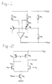
- Figure 1 by way of comparison shows an arrangement known per se , in which the MOS transistors of the differential amplifier have to operate in the in triode regions and in which in the case of integration a substantial portion of the chip area is occupied the resistors.
- Figure 2 shows diagrammatically the principal components of the differential amplifier.
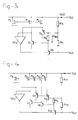
- Figure 3 shows a first embodiment of an arrangement in accordance with the invention.
- Figure 4 shows an embodiment of an arrangement as shown in Figure 3, employing two arrays comprising two transistors each.
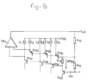
- Figure 5 shows a second embodiment of the arrangement in accordance with the invention, which also utilizes transistor arrays.
- the circuit arrangement shown in Figure 1 comprises a MOS differential amplifier OA1, the transistors Q1 and Q2 and the resistors R1 to R5.
- the transistor Q1 is connected to the power supply V DD in series with the resistor R3.
- the transistor Q2 in series with the resistors R1 and R2 is connected to the power supply V DD .
- the bases of the two transistors Q1 and Q2 are interconnected and are driven by the voltage on the junction point of the series arrangement of the resistors R4 and R5, which is arranged between the power supply V DD and the output terminal on which the output voltage V out is available.
- the inputs of the differential amplifier are respectively connected to the junction point between Q1 and R3 and the junction point between R1 and R2.
- the output of the differential amplifier is connected to the output terminal V out .
- the collectors of the two transistors Q1, Q2 are connected to the negative supply voltage, for example earth, if required via further components, not shown, which may form part of a further circuit utilizing the reference-voltage to be generated. In the simplest case the two collectors are connected directly to the aid negative supply voltage.
- the voltage on the bases of the transistors Q2, Q1 is equal to the positive supply voltage V DD minus the band-gap reference-voltage of approximately 1.3 V.
- the common-mode input voltage of the differential amplifier OA1 is then equal to V DD - 1.3 V + V BEQ1 ⁇ V DD - 0.7 V , which is too high, so that the MOS transistors in the differential amplifier OA1 have to operate in their triode regions.
- the gain of the differential amplifier is comparatively small, which has an adverse effect on the correct operation of the arrangement.
- FIG. 2 shows diagrammatically the principal components of the differential amplifier, i.e. the MOS transistors P8 to P11.
- the two transistors P10 and P11 constitute a current mirror for supplying currents to the input transistors P8 and P9, which are connected to the two inputs IN1 and IN2.
- the transistor P12 provides the current setting and is controlled by the bias voltage V bias .
- the output signal is then available on the output out.
- MOS differential amplifier reference is made to the literature well-known to those skilled in the art. By way of example reference is made to the article "An integrated Single Chip PCM Voice codec with filters", IEEE Journal of Solid State Circuits, Vol. Se-16, no. 4, August, 1981, page 330, Figure 13.
- FIG 3 shows a first embodiment of a circuit arrangement in accordance with the invention in which the common-mode input voltage of the differential amplifier is at a lower voltage level relative to the positive supply voltage V DD than in the arrangement shown in Figure 1.
- This arrangement again comprises the MOS differential amplifier OA2, the bipolar transistors Q3, Q4, Q5, the resistors R6, R7, R8, and the MOS transistors P1, P2 and P3.
- the transistors P1 and P2 together with the current source transistor P3 are arranged in a current mirror circuit and are connected to the power supply voltage V DD .
- the transistors P1, P2 and P3 are dimensioned in such a way that for a predetermined current through P3 a desired first current flows through P1 and a desired second current through P2.
- P1 is arranged in series with Q3, so that the first current also flows through Q3 and P2 is arranged in series with Q4 so that the second current also flows through Q4.
- the junction point between P1 and Q3 is connected to one input of the differential amplifier OA2 and the junction point between P2 and Q4 is connected to the other input of the differential amplifier OA2.
- the bases of the transistors Q3 and Q4 are each connected to a terminal of the resistor R6.
- the base of Q3 is connected to the emitter of Q5 whose base is driven by the output of the differential amplifier OA2.
- the base of Q5 is further connected to the resistor R7, which is arranged in series with the resistor R8 between the power supply V DD and the output junction point on which the output voltage V out is available.
- the junction point between R7 and R8 is connected to the base of Q4.
- the collectors of the transistors Q3, Q4, Q5 are connected to the negative supply voltage (for example earth) either directly of via component of the circuit of which the reference
- the currents through the transistors Q3 and Q4 and the appropriate dimensioning of Q4 ensure that different base emitter voltages ⁇ V BE are produced across the two transistors.
- the difference between the two base emitter voltages ⁇ V BE appears across the resistor R6.
- the operational amplifier OA2 tends to influence the current through R6 in such a way that a balanced situation is obtained in which the arrangement in a manner known per se can function as a band-gap reference-voltage arrangement.
- the difference with the known arrangement resides in the fact that in the present arrangement the common-mode input voltage appears on the inputs of the differential amplifier OA2.
- FIG. 4 shows a second embodiment of an arrangement in accordance with the invention, which instead of the transistors Q3 and Q4 employs a cascade arrangement comprising the transistors Q6 and Q8 and Q7 and Q9 respectively.
- Each of said transistors Q6 to Q9 is connected to the power supply line V DD in series with a separate MOS transistor P4 to P7.
- the MOS transistors P4 to P7 are arranged as a current mirror circuit controlled by the current source transistor P8 in such a way that a first current flows through each of the transistors Q6 and Q8 and a second current flows through each of the transistors Q7 and Q9.
- a further reduction of the effect of offset can be achieved by using three or more transistors in each of the cascade arrangements. It will be evident that depending on the magnitude of the voltage across the resistors R10 and R11 this is at the expense of the improvement in common-mode input voltage. However, under specific circumstances it may be preferred to utilize cascade circuits comprising larger numbers of transistors.
- Figure 5 shows a second embodiment of an arrangement in accordance with the invention, comprising a cascade circuit comprising j transistors.
- the base of the transistor Q13 is connected to the negative supply voltage in the present earth, and the output of the differential amplifier OA4 is connected to the output terminal. Now this results in a positive reference-voltage V out relative to earth being generated.
- the arrangement shown in Figure 5 comprises said differential amplifier OA4, the transistors Q11a...Q11c constituting the first array, the transistors Q12a...Q12c constituting the second array, and the transistor Q13.
- the arrangement further comprises the resistors R12, R13 and R14, which perform the same functions as the resistors R9, R10, R11 in Figure 4.
- the MOS transistors which are operated as current source transistors, are not shown separately but are represented diagrammatically as the current sources I1 to I6. Again the further connections between the collectors of the bipolar transistors Q11a...Q11c, Q12a...Q12c, Q13 to a negative supply voltage are not shown.
- each cascade circuit comprises j transistors a voltage j ⁇ V BE will be generated across the resistor R12.
- V out g [V BE (Q13) + n.j. ⁇ V BE + n.V. os ]
- V BE basis-emitter voltage
- differential amplifier may be of any other construction than that shown in Figure 2.
- transistors may be replaced by transistors of the opposite conductivity type.
Landscapes
- Engineering & Computer Science (AREA)
- Physics & Mathematics (AREA)
- Microelectronics & Electronic Packaging (AREA)
- Electromagnetism (AREA)
- General Physics & Mathematics (AREA)
- Radar, Positioning & Navigation (AREA)
- Automation & Control Theory (AREA)
- Power Engineering (AREA)
- Nonlinear Science (AREA)
- Amplifiers (AREA)
- Control Of Electrical Variables (AREA)
Claims (5)
- Circuit de tension de référence d'écart de bande comportant- un amplificateur différentiel MOS (OA1; OA2; OA3; OA4) ayant une première et une seconde entrée, ainsi qu'une sortie,- un premier transistor bipolaire (Q1; Q3; Q6, Q8; Q11a, Q11b, Q11c) dont le trajet de base-émetteur est disposé entre la première entrée de l'amplificateur différentiel (OA1; OA2; OA3; OA4) et un premier point commun et dont le trajet d'émetteur-collecteur est disposé dans un premier trajet de courant (Q1, R3; Q3, P1; Q8, P6; Q11c, I5) pour conduire un premier courant,- un deuxième transistor bipolaire (Q2; Q4; Q7, Q9; Q12a, Q12b, Q12c) dont le trajet de base-émetteur en série avec une première résistance (R1; R6; R9; R12) est disposé entre la seconde entrée de l'amplificateur différentiel (OA1; OA2; OA3; OA4) et le premier point commun et dont le trajet d'émetteur-collecteur est disposé dans un deuxième trajet de courant (Q2, R2; Q4, P2; Q9, P7; Q12c, I6) pour conduire un deuxième courant,- un montage série d'une deuxième (R4; R8; R11; R14) et d'une troisième résistance (R5; R7; R10; R13) disposé entre une borne de tension d'alimentation (VDD; masse) et une borne de sortie (Vout) du circuit pour prélever une tension de référence, un deuxième point commun à la deuxième (R4; R8, R11; R14) et à la troisième (R5; R7; R10; R13) résistance étant couplé à la base du deuxième transistor (Q2; Q4; Q7; Q9; Q12a, Q12b, Q12c), la sortie de l'amplificateur différentiel (OA1; OA2; OA3; OQ4) étant couplée à la borne de sortie (Vout) du circuit et- des moyens pour fournir respectivement les premier et deuxième courants par les premier (Q1, R3; Q3, P1; Q8, P6; Q11c, I5) et deuxième (Q2, R2; Q4, P2; Q9, P7; Q12c, I6) trajets de courant, la première résistance (R1; R6; R9; R12) étant disposée entre la base du deuxième transistor (Q2; Q4, Q7, Q9; Q12a, Q12b, Q12c) et le premier point commun,caractérisé en ce que le premier point commun est couplé par un trajet de base-émetteur d'un troisième transistor (Q5; Q10; Q13) à une extrémité du montage série de la deuxième (R4; R8; R11; R14) et de la troisième (R5; R7; R10; R13) résistance.
- Circuit de tension de référence d'écart de bande selon la revendication 1, caractérisé en ce que la base du troisième transistor (Q5; Q10) est couplée à la borne de sortie (Vout) du circuit.
- Circuit de tension de référence d'écart de bande selon la revendication 1, caractérisé en ce que la base du troisième transistor (Q13) est couplée à une autre borne de tension d'alimentation (masse).
- Circuit de tension de référence d'écart de bande selon la revendication 1, 2 ou 3, caractérisé en ce que les premier (Q1; Q3; Q6; Q8; Q11a, Q11b, Q11c) et deuxième (Q2; Q4; Q7; Q9; Q12a, Q12b, Q12c) transistors sont remplacés par des premier (Q6, Q8; Q11a, Q11b, Q11c) et deuxième (Q7, Q9; Q12a, Q12b, Q12c) réseaux de transistors, le nombre de transistors du premier (Q6, Q8; Q11a, Q11b, Q11c) et du deuxième (Q7, Q9; Q12a, Q12b, Q12c) réseau étant égal et les transistors du premier (Q6, Q8; Q11a, Q11b, Q11c) et du deuxième (Q7, Q9; Q12a, Q12c, Q12c) réseau étant interconnectés de façon que chaque transistor (Q6, Q8; Q11a, Q11b, Q11c; Q7, Q9; Q12a, Q12b, Q12c) a son trajet de collecteur-émetteur disposé dans un trajet de courant (Q6, P4; Q7, P5; Q8, P6; Q9, P7; Q11a, I1; Q11b, I2; Q11c, I3; Q12a; I4; Q12b, I5; Q12c, I6) pour conduire respectivement les premier et deuxième courants et sa base reliée à un émetteur d'un transistor suivant, l'émetteur du dernier transistor (Q6, Q7; Q11a, Q12a) du premier (Q6, Q8; Q11a, Q11b, Q11c) et du deuxième (Q7, Q9; Q12a, Q12b, Q12c) réseau étant relié à une entrée respective de l'amplificateur différentiel (OA1; OA2; OA3; OA4), et la base du premier transistor (Q1, Q9; Q11c, Q12c) du premier (Q6, Q8; Q11a, Q11b, Q11c) et du deuxième (Q7, Q9; Q12a, Q12b, Q12c) réseau étant respectivement reliée au premier point commun et à la première résistance (R1; R6; R9; R12).
- Circuit de tension de référence d'écart de bande selon la revendication 4, caractérisé en ce que le nombre de transistors du premier (Q6, Q8) et du deuxième (Q7, Q9) réseau est égal à deux.
Applications Claiming Priority (2)
| Application Number | Priority Date | Filing Date | Title |
|---|---|---|---|
| NL8800422 | 1988-02-19 | ||
| NL8800422 | 1988-02-19 |
Publications (2)
| Publication Number | Publication Date |
|---|---|
| EP0329247A1 EP0329247A1 (fr) | 1989-08-23 |
| EP0329247B1 true EP0329247B1 (fr) | 1993-12-29 |
Family
ID=19851819
Family Applications (1)
| Application Number | Title | Priority Date | Filing Date |
|---|---|---|---|
| EP89200344A Expired - Lifetime EP0329247B1 (fr) | 1988-02-19 | 1989-02-14 | Circuit de tension de référence à bande interdite |
Country Status (5)
| Country | Link |
|---|---|
| US (1) | US4897595A (fr) |
| EP (1) | EP0329247B1 (fr) |
| JP (1) | JP2747313B2 (fr) |
| KR (1) | KR0136873B1 (fr) |
| DE (1) | DE68911708T2 (fr) |
Families Citing this family (16)
| Publication number | Priority date | Publication date | Assignee | Title |
|---|---|---|---|---|
| KR100188821B1 (ko) * | 1990-08-20 | 1999-06-01 | 사와무라 시코 | 정전압발생회로 |
| DE4111103A1 (de) * | 1991-04-05 | 1992-10-08 | Siemens Ag | Cmos-bandabstands-referenzschaltung |
| DE69423742T2 (de) * | 1994-04-29 | 2000-08-31 | Sgs-Thomson Microelectronics, Inc. | Bandabstands-Referenzschaltung |
| US5459427A (en) * | 1994-05-06 | 1995-10-17 | Motorola, Inc. | DC level shifting circuit for analog circuits |
| US5757224A (en) * | 1996-04-26 | 1998-05-26 | Caterpillar Inc. | Current mirror correction circuitry |
| US5952873A (en) * | 1997-04-07 | 1999-09-14 | Texas Instruments Incorporated | Low voltage, current-mode, piecewise-linear curvature corrected bandgap reference |
| US5945873A (en) * | 1997-12-15 | 1999-08-31 | Caterpillar Inc. | Current mirror circuit with improved correction circuitry |
| US6031365A (en) * | 1998-03-27 | 2000-02-29 | Vantis Corporation | Band gap reference using a low voltage power supply |
| US6100667A (en) * | 1999-01-21 | 2000-08-08 | National Semiconductor Corporation | Current-to-voltage transition control of a battery charger |
| DE10006950C1 (de) * | 2000-02-16 | 2002-01-24 | Infineon Technologies Ag | Schaltungsanordnung zur Konstantspannungs- und / oder Konstantstromerzeugung |
| US6657480B2 (en) * | 2000-07-21 | 2003-12-02 | Ixys Corporation | CMOS compatible band gap reference |
| US6288525B1 (en) * | 2000-11-08 | 2001-09-11 | Agere Systems Guardian Corp. | Merged NPN and PNP transistor stack for low noise and low supply voltage bandgap |
| JP4513209B2 (ja) * | 2000-12-28 | 2010-07-28 | 富士電機システムズ株式会社 | 半導体集積回路 |
| JP4064799B2 (ja) * | 2002-12-04 | 2008-03-19 | 旭化成エレクトロニクス株式会社 | 定電圧発生回路 |
| US6864741B2 (en) * | 2002-12-09 | 2005-03-08 | Douglas G. Marsh | Low noise resistorless band gap reference |
| US7211993B2 (en) * | 2004-01-13 | 2007-05-01 | Analog Devices, Inc. | Low offset bandgap voltage reference |
Family Cites Families (5)
| Publication number | Priority date | Publication date | Assignee | Title |
|---|---|---|---|---|
| US4071813A (en) * | 1974-09-23 | 1978-01-31 | National Semiconductor Corporation | Temperature sensor |
| US4249122A (en) * | 1978-07-27 | 1981-02-03 | National Semiconductor Corporation | Temperature compensated bandgap IC voltage references |
| US4287439A (en) * | 1979-04-30 | 1981-09-01 | Motorola, Inc. | MOS Bandgap reference |
| US4317054A (en) * | 1980-02-07 | 1982-02-23 | Mostek Corporation | Bandgap voltage reference employing sub-surface current using a standard CMOS process |
| US4380706A (en) * | 1980-12-24 | 1983-04-19 | Motorola, Inc. | Voltage reference circuit |
-
1989
- 1989-02-14 EP EP89200344A patent/EP0329247B1/fr not_active Expired - Lifetime
- 1989-02-14 DE DE68911708T patent/DE68911708T2/de not_active Expired - Fee Related
- 1989-02-16 KR KR1019890001763A patent/KR0136873B1/ko not_active Expired - Fee Related
- 1989-02-17 US US07/312,505 patent/US4897595A/en not_active Expired - Fee Related
- 1989-02-17 JP JP1036413A patent/JP2747313B2/ja not_active Expired - Lifetime
Also Published As
| Publication number | Publication date |
|---|---|
| DE68911708D1 (de) | 1994-02-10 |
| JPH01246614A (ja) | 1989-10-02 |
| JP2747313B2 (ja) | 1998-05-06 |
| EP0329247A1 (fr) | 1989-08-23 |
| KR0136873B1 (ko) | 1998-05-15 |
| US4897595A (en) | 1990-01-30 |
| KR890013543A (ko) | 1989-09-23 |
| DE68911708T2 (de) | 1994-06-30 |
Similar Documents
| Publication | Publication Date | Title |
|---|---|---|
| US4447784A (en) | Temperature compensated bandgap voltage reference circuit | |
| US5867012A (en) | Switching bandgap reference circuit with compounded ΔV.sub.βΕ | |
| US4399399A (en) | Precision current source | |
| US4897595A (en) | Band-gap reference voltage circuit with feedback to reduce common mode voltage | |
| US5432432A (en) | Reference voltage generating circuit with temperature stability for use in CMOS integrated circuits | |
| US5448158A (en) | PTAT current source | |
| US4935690A (en) | CMOS compatible bandgap voltage reference | |
| WO1998048334A9 (fr) | Circuit de reference de precision a largeur de bande interdite | |
| EP0396996A2 (fr) | Circuit de seuil à bande interdite avec hystérésis | |
| EP0329232B1 (fr) | Sources de tension et de courant stabilisées | |
| US4524318A (en) | Band gap voltage reference circuit | |
| US4978868A (en) | Simplified transistor base current compensation circuitry | |
| US4591804A (en) | Cascode current-source arrangement having dual current paths | |
| EP0472128B1 (fr) | Circuit de génération de tension constante | |
| US4924113A (en) | Transistor base current compensation circuitry | |
| EP0596653B1 (fr) | Circuit générateur de courant de référence à tension faible | |
| JPH07152445A (ja) | 電圧発生回路 | |
| EP0156410B1 (fr) | Montage amplificateur | |
| EP0456127B1 (fr) | Amplificateur | |
| US4485313A (en) | Low-value current source circuit | |
| US4524330A (en) | Bipolar circuit for amplifying differential signal | |
| JPH08139531A (ja) | 差動アンプ | |
| US5166638A (en) | Differential amplifier having output stage quickly brought into inactive condition by a control signal | |
| JP2772069B2 (ja) | 定電流回路 | |
| JPH06250751A (ja) | 基準電圧回路 |
Legal Events
| Date | Code | Title | Description |
|---|---|---|---|
| PUAI | Public reference made under article 153(3) epc to a published international application that has entered the european phase |
Free format text: ORIGINAL CODE: 0009012 |
|
| AK | Designated contracting states |
Kind code of ref document: A1 Designated state(s): DE FR GB IT NL |
|
| 17P | Request for examination filed |
Effective date: 19900222 |
|
| 17Q | First examination report despatched |
Effective date: 19920703 |
|
| GRAA | (expected) grant |
Free format text: ORIGINAL CODE: 0009210 |
|
| AK | Designated contracting states |
Kind code of ref document: B1 Designated state(s): DE FR GB IT NL |
|
| PG25 | Lapsed in a contracting state [announced via postgrant information from national office to epo] |
Ref country code: NL Effective date: 19931229 |
|
| REF | Corresponds to: |
Ref document number: 68911708 Country of ref document: DE Date of ref document: 19940210 |
|
| ITTA | It: last paid annual fee | ||
| ITF | It: translation for a ep patent filed | ||
| ET | Fr: translation filed | ||
| NLV1 | Nl: lapsed or annulled due to failure to fulfill the requirements of art. 29p and 29m of the patents act | ||
| PLBE | No opposition filed within time limit |
Free format text: ORIGINAL CODE: 0009261 |
|
| STAA | Information on the status of an ep patent application or granted ep patent |
Free format text: STATUS: NO OPPOSITION FILED WITHIN TIME LIMIT |
|
| 26N | No opposition filed | ||
| ITPR | It: changes in ownership of a european patent |
Owner name: CAMBIO RAGIONE SOCIALE;PHILIPS ELECTRONICS N.V. |
|
| REG | Reference to a national code |
Ref country code: FR Ref legal event code: CD |
|
| REG | Reference to a national code |
Ref country code: FR Ref legal event code: CD |
|
| PGFP | Annual fee paid to national office [announced via postgrant information from national office to epo] |
Ref country code: FR Payment date: 20000222 Year of fee payment: 12 |
|
| PGFP | Annual fee paid to national office [announced via postgrant information from national office to epo] |
Ref country code: GB Payment date: 20000228 Year of fee payment: 12 |
|
| PGFP | Annual fee paid to national office [announced via postgrant information from national office to epo] |
Ref country code: DE Payment date: 20000419 Year of fee payment: 12 |
|
| PG25 | Lapsed in a contracting state [announced via postgrant information from national office to epo] |
Ref country code: GB Free format text: LAPSE BECAUSE OF NON-PAYMENT OF DUE FEES Effective date: 20010214 |
|
| GBPC | Gb: european patent ceased through non-payment of renewal fee |
Effective date: 20010214 |
|
| PG25 | Lapsed in a contracting state [announced via postgrant information from national office to epo] |
Ref country code: FR Free format text: LAPSE BECAUSE OF NON-PAYMENT OF DUE FEES Effective date: 20011031 |
|
| REG | Reference to a national code |
Ref country code: FR Ref legal event code: ST |
|
| PG25 | Lapsed in a contracting state [announced via postgrant information from national office to epo] |
Ref country code: DE Free format text: LAPSE BECAUSE OF NON-PAYMENT OF DUE FEES Effective date: 20011201 |
|
| PG25 | Lapsed in a contracting state [announced via postgrant information from national office to epo] |
Ref country code: IT Free format text: LAPSE BECAUSE OF NON-PAYMENT OF DUE FEES;WARNING: LAPSES OF ITALIAN PATENTS WITH EFFECTIVE DATE BEFORE 2007 MAY HAVE OCCURRED AT ANY TIME BEFORE 2007. THE CORRECT EFFECTIVE DATE MAY BE DIFFERENT FROM THE ONE RECORDED. Effective date: 20050214 |