EP0331148B1 - Mikroskop - Google Patents
Mikroskop Download PDFInfo
- Publication number
- EP0331148B1 EP0331148B1 EP89103590A EP89103590A EP0331148B1 EP 0331148 B1 EP0331148 B1 EP 0331148B1 EP 89103590 A EP89103590 A EP 89103590A EP 89103590 A EP89103590 A EP 89103590A EP 0331148 B1 EP0331148 B1 EP 0331148B1
- Authority
- EP
- European Patent Office
- Prior art keywords
- tip
- objective lens
- optical axis
- sample
- optical
- Prior art date
- Legal status (The legal status is an assumption and is not a legal conclusion. Google has not performed a legal analysis and makes no representation as to the accuracy of the status listed.)
- Expired - Lifetime
Links
- 230000003287 optical effect Effects 0.000 claims description 85
- 239000011521 glass Substances 0.000 claims description 19
- 230000000694 effects Effects 0.000 claims 2
- 239000010408 film Substances 0.000 description 9
- 239000000919 ceramic Substances 0.000 description 6
- 230000004048 modification Effects 0.000 description 5
- 238000012986 modification Methods 0.000 description 5
- 238000001514 detection method Methods 0.000 description 4
- BASFCYQUMIYNBI-UHFFFAOYSA-N platinum Chemical compound [Pt] BASFCYQUMIYNBI-UHFFFAOYSA-N 0.000 description 4
- 238000005286 illumination Methods 0.000 description 3
- WABPQHHGFIMREM-UHFFFAOYSA-N lead(0) Chemical compound [Pb] WABPQHHGFIMREM-UHFFFAOYSA-N 0.000 description 3
- 239000004065 semiconductor Substances 0.000 description 3
- IJGRMHOSHXDMSA-UHFFFAOYSA-N Atomic nitrogen Chemical compound N#N IJGRMHOSHXDMSA-UHFFFAOYSA-N 0.000 description 2
- 239000012298 atmosphere Substances 0.000 description 2
- 238000005452 bending Methods 0.000 description 2
- PCHJSUWPFVWCPO-UHFFFAOYSA-N gold Chemical compound [Au] PCHJSUWPFVWCPO-UHFFFAOYSA-N 0.000 description 2
- 229910052737 gold Inorganic materials 0.000 description 2
- 239000010931 gold Substances 0.000 description 2
- 230000001788 irregular Effects 0.000 description 2
- 239000007788 liquid Substances 0.000 description 2
- 238000005259 measurement Methods 0.000 description 2
- 230000002093 peripheral effect Effects 0.000 description 2
- 229910052697 platinum Inorganic materials 0.000 description 2
- XLYOFNOQVPJJNP-UHFFFAOYSA-N water Substances O XLYOFNOQVPJJNP-UHFFFAOYSA-N 0.000 description 2
- 241001052209 Cylinder Species 0.000 description 1
- 239000007767 bonding agent Substances 0.000 description 1
- 238000005219 brazing Methods 0.000 description 1
- 239000004020 conductor Substances 0.000 description 1
- 238000010276 construction Methods 0.000 description 1
- 230000001419 dependent effect Effects 0.000 description 1
- 238000000151 deposition Methods 0.000 description 1
- 238000010586 diagram Methods 0.000 description 1
- 238000003754 machining Methods 0.000 description 1
- 238000004519 manufacturing process Methods 0.000 description 1
- 238000000034 method Methods 0.000 description 1
- 238000000386 microscopy Methods 0.000 description 1
- 229910052757 nitrogen Inorganic materials 0.000 description 1
- 238000005498 polishing Methods 0.000 description 1
- 238000004544 sputter deposition Methods 0.000 description 1
- 239000010409 thin film Substances 0.000 description 1
- WFKWXMTUELFFGS-UHFFFAOYSA-N tungsten Chemical compound [W] WFKWXMTUELFFGS-UHFFFAOYSA-N 0.000 description 1
- 229910052721 tungsten Inorganic materials 0.000 description 1
- 239000010937 tungsten Substances 0.000 description 1
- 230000005641 tunneling Effects 0.000 description 1
Images



Classifications
-
- G—PHYSICS
- G01—MEASURING; TESTING
- G01Q—SCANNING-PROBE TECHNIQUES OR APPARATUS; APPLICATIONS OF SCANNING-PROBE TECHNIQUES, e.g. SCANNING PROBE MICROSCOPY [SPM]
- G01Q60/00—Particular types of SPM [Scanning Probe Microscopy] or microscopes; Essential components thereof
- G01Q60/18—SNOM [Scanning Near-Field Optical Microscopy] or apparatus therefor, e.g. SNOM probes
- G01Q60/22—Probes, their manufacture, or their related instrumentation, e.g. holders
-
- B—PERFORMING OPERATIONS; TRANSPORTING
- B82—NANOTECHNOLOGY
- B82Y—SPECIFIC USES OR APPLICATIONS OF NANOSTRUCTURES; MEASUREMENT OR ANALYSIS OF NANOSTRUCTURES; MANUFACTURE OR TREATMENT OF NANOSTRUCTURES
- B82Y20/00—Nanooptics, e.g. quantum optics or photonic crystals
-
- B—PERFORMING OPERATIONS; TRANSPORTING
- B82—NANOTECHNOLOGY
- B82Y—SPECIFIC USES OR APPLICATIONS OF NANOSTRUCTURES; MEASUREMENT OR ANALYSIS OF NANOSTRUCTURES; MANUFACTURE OR TREATMENT OF NANOSTRUCTURES
- B82Y35/00—Methods or apparatus for measurement or analysis of nanostructures
-
- G—PHYSICS
- G01—MEASURING; TESTING
- G01Q—SCANNING-PROBE TECHNIQUES OR APPARATUS; APPLICATIONS OF SCANNING-PROBE TECHNIQUES, e.g. SCANNING PROBE MICROSCOPY [SPM]
- G01Q10/00—Scanning or positioning arrangements, i.e. arrangements for actively controlling the movement or position of the probe
- G01Q10/04—Fine scanning or positioning
-
- G—PHYSICS
- G01—MEASURING; TESTING
- G01Q—SCANNING-PROBE TECHNIQUES OR APPARATUS; APPLICATIONS OF SCANNING-PROBE TECHNIQUES, e.g. SCANNING PROBE MICROSCOPY [SPM]
- G01Q30/00—Auxiliary means serving to assist or improve the scanning probe techniques or apparatus, e.g. display or data processing devices
- G01Q30/02—Non-SPM analysing devices, e.g. SEM [Scanning Electron Microscope], spectrometer or optical microscope
- G01Q30/025—Optical microscopes coupled with SPM
-
- G—PHYSICS
- G01—MEASURING; TESTING
- G01Q—SCANNING-PROBE TECHNIQUES OR APPARATUS; APPLICATIONS OF SCANNING-PROBE TECHNIQUES, e.g. SCANNING PROBE MICROSCOPY [SPM]
- G01Q60/00—Particular types of SPM [Scanning Probe Microscopy] or microscopes; Essential components thereof
- G01Q60/02—Multiple-type SPM, i.e. involving more than one SPM techniques
-
- G—PHYSICS
- G01—MEASURING; TESTING
- G01Q—SCANNING-PROBE TECHNIQUES OR APPARATUS; APPLICATIONS OF SCANNING-PROBE TECHNIQUES, e.g. SCANNING PROBE MICROSCOPY [SPM]
- G01Q60/00—Particular types of SPM [Scanning Probe Microscopy] or microscopes; Essential components thereof
- G01Q60/10—STM [Scanning Tunnelling Microscopy] or apparatus therefor, e.g. STM probes
- G01Q60/16—Probes, their manufacture, or their related instrumentation, e.g. holders
-
- G—PHYSICS
- G01—MEASURING; TESTING
- G01Q—SCANNING-PROBE TECHNIQUES OR APPARATUS; APPLICATIONS OF SCANNING-PROBE TECHNIQUES, e.g. SCANNING PROBE MICROSCOPY [SPM]
- G01Q70/00—General aspects of SPM probes, their manufacture or their related instrumentation, insofar as they are not specially adapted to a single SPM technique covered by group G01Q60/00
- G01Q70/02—Probe holders
-
- G—PHYSICS
- G02—OPTICS
- G02B—OPTICAL ELEMENTS, SYSTEMS OR APPARATUS
- G02B21/00—Microscopes
- G02B21/0004—Microscopes specially adapted for specific applications
- G02B21/002—Scanning microscopes
-
- Y—GENERAL TAGGING OF NEW TECHNOLOGICAL DEVELOPMENTS; GENERAL TAGGING OF CROSS-SECTIONAL TECHNOLOGIES SPANNING OVER SEVERAL SECTIONS OF THE IPC; TECHNICAL SUBJECTS COVERED BY FORMER USPC CROSS-REFERENCE ART COLLECTIONS [XRACs] AND DIGESTS
- Y10—TECHNICAL SUBJECTS COVERED BY FORMER USPC
- Y10S—TECHNICAL SUBJECTS COVERED BY FORMER USPC CROSS-REFERENCE ART COLLECTIONS [XRACs] AND DIGESTS
- Y10S977/00—Nanotechnology
- Y10S977/84—Manufacture, treatment, or detection of nanostructure
- Y10S977/849—Manufacture, treatment, or detection of nanostructure with scanning probe
- Y10S977/86—Scanning probe structure
- Y10S977/861—Scanning tunneling probe
-
- Y—GENERAL TAGGING OF NEW TECHNOLOGICAL DEVELOPMENTS; GENERAL TAGGING OF CROSS-SECTIONAL TECHNOLOGIES SPANNING OVER SEVERAL SECTIONS OF THE IPC; TECHNICAL SUBJECTS COVERED BY FORMER USPC CROSS-REFERENCE ART COLLECTIONS [XRACs] AND DIGESTS
- Y10—TECHNICAL SUBJECTS COVERED BY FORMER USPC
- Y10S—TECHNICAL SUBJECTS COVERED BY FORMER USPC CROSS-REFERENCE ART COLLECTIONS [XRACs] AND DIGESTS
- Y10S977/00—Nanotechnology
- Y10S977/84—Manufacture, treatment, or detection of nanostructure
- Y10S977/849—Manufacture, treatment, or detection of nanostructure with scanning probe
- Y10S977/86—Scanning probe structure
- Y10S977/868—Scanning probe structure with optical means
- Y10S977/869—Optical microscope
Definitions
- the present invention relates to a microscope apparatus as defined in the preamble of claim 1 or claim 18, respectively, for observing finely detailed objects such as semiconductor structures.
- a high-resolution scanning tunnel microscope (hereinafter referred to as an STM) has recently been developed for the observation of finely detailed objects.
- the STM has a resolution high enough to enable observation of, for example, atoms, and comprises a tip which is attached to a microscope body.
- the tip is placed approximately 1 »m from the sample to be observed, so that electron clouds of the atoms of the distal end of the tip and those of the sample overlap one another, and a tunnel current is then caused to flow between the tip and the sample when a voltage is applied between them. Since the value of the tunnel current changes exponentially in accordance with the distance between the tip and the sample, therefore the STM utilizes the relationship between tunnel current and distance for observation of the sample.
- the STM two-dimensionally scans the surface of the sample by means of the tip, measuring the size of the tunnel current at various measuring points on the sample surface. Based on the measured values of the tunnel current, the distance between the tip at each measuring point and the sample of observation is superaccurately measured, and the measured values of distance at the individual measuring points are plotted to obtain a three-dimensional image of the sample surface.
- the tip is moved up and down for tracing the irregular configuration of the sample surface with two-dimentionally scanning the sample surface, so that the distance between the surface and the tip, and the tunnel current are constant.
- the three-dimensional image of the sample surface is obtained on the basis of the amount of the up-and-down motion of the tip.
- the observation area of the above STM usually ranges from tens of nanometers square to about 1 »m square.
- a desired observation image can be obtained at any region of the sample surface. In this case, therefore, the observation region need not be specially chosen.
- the configuration of the observation surface is irregular, as in the case of observing the profile of a semiconductor device formed of a wafer carrying thereon a linear pattern 1 »m wide and 0.4 »m high, for example, the tip must be accurately located in a specified place for observation.
- the conventional STM cannot attain this.
- an improved apparatus which combines an STM with a scanning electron microscope (SEM).
- SEM scanning electron microscope
- an optical microscope is arranged diagonally behind an STM, and the tip of the STM is positioned at a desired observation region of the surface of a sample to be observed while the tip and the sample are being observed by the optical microscope.
- the optical microscope is designed for diagonal observation of a sample from behind, so that it is difficult to obtain high magnifying power and it is difficult to accurately observe the relationship betwen the tip and the sample surface by the optical microscope. Thus, the tip cannot be accurately positioned with respect to the sample of observation.
- Another scanning type tunnel microscope is described in the not prebublished document EP-A-0 406 413.
- this apparatus comprising a combination of an optical microscope with a tunnel scanning unit an objective lens and a conductive tunnel tip of the tunnel scanning unit are disposed in such a manner that the center axis of the tunnel tip is in alignment with the optical axis of the optical microscope.
- Observation of sample surfaces is performed by moving both the sample and the tunnel tip in the axial direction whereby the tunnel tip is mounted and moved by a three-dimensional actuator. Focusing is made by independently moving the objective lens of the optical microscope in the axial direction.
- the tip of the scanning tunnel microscope unit Since the tunnel tip and the objective lens are not connected but moved independently, the tip of the scanning tunnel microscope unit has to be aligned with the optical unit in a complicated operation before each observation. Moreover, there exists a possibility that objective lens and tip holder touch erroneously during alignment operations and are thus damaged.
- the present invention has been developed in consideration of the above-described circumstances, and has as its object to provide a microscope apparatus which is capable of accurately, fast and safely positioning a tip at a specified location for observation, and which enables accurate high-magnification observation of the structure of the object being observed.
- an apparatus comprises: the features of claims 1 or 18, respectively. Preferred embodiments of the apparatus of the invention are described in the dependent claims.
- the tip can be accurately positioned at a specified location of a sample to be observed within the field of vision of the optical microscope body, while the sample is being visually observed through the microscope body.
- a specified region of the sample can be accurately observed while the sample and the tip are being shifted relative to each other.
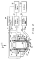
- Figs. 1 to 4 show a microscope apparatus according to a first embodiment of the present invention.
- the apparatus comprises vertical illumination type bright-field optical microscope body 10 which includes substantially T-shaped body tube 12 which has vertical section 12a and horizontal section 12b. Tube 12 is supported, in the state as illustrated, by a supporting mechanism (not shown).
- Eyepiece section 14 is formed at a top opening portion of vertical section 12a, and industrial television (ITV) camera 16 is mounted on the eyepiece section.
- Unit mounting section 18 is formed at a bottom opening portion of vertical section 12a, and observation unit 20 (mentioned later) is fitted to the mounting section.
- half mirror 21 is provided at the middle portion of vertical section 12a.
- Mounting section 22 is formed at an end opening portion of horizontal section 12b, and illuminator 24 having lamp 23 is mounted on section 22 so as to face mirror 21.
- Sample stage 26 is positioned opposing the bottom of observation unit 20, at a predetermined distance therefrom.
- a light beam from illuminator 24 is deflected downward by half mirror 21, so as to be incident on observation surface 28a of object 28 placed on sample stage 26.
- An image of object 28 is transmitted through observation unit 20, to be imaged on the side of eyepiece section 14, so that it can be observed through camera 16.
- observation unit 20 is provided with objective lens unit 30 and tip unit 32.
- Unit 30 includes cylindrical lens holder 34, in which objective lens optical system 35 is arranged.
- System 35 includes objective lens 36 fixed to the lower end of holder 34.
- Male screw portion 34a which is formed at the upper end portion of holder 34, is threaded in female screw portion 18a formed on mounting section 18 of body 10.
- unit 30 is removably fitted to section 18 and such that the optical axis of optical system 35 is in alignment with the axis of the light beam from illuminator 24.
- Tip unit 32 includes tip 38 (mentioned later), piezoelectric section 40, and support cylinder 42 supporting these two elements.
- Cylinder 42 has upper and lower cylinderes 42a and 42b, between which ring-shaped piezoelectric section 40 is fixed.
- Male screw portion 44 which is formed at the upper end portion of upper cylinder 42a, is threaded in female screw portion 18b formed on mounting section 18 of body 10.
- support cylinder 42 is fitted to section 18 so that it is situated with a gap outside lens holder 34, and its position can be independently adjusted along the optical axis of optical system 35.
- Female screw portions 18a and 18b of mounting section 18 have the same diameter.
- a light transmitting member e.g., glass plate 48
- Tip 38 is fixed to plate 48.
- Tip 38 is formed by sharpening the distal end of a tip of tungsten or platinum, with a length of several millimeters to tens of millimeters and a diameter of several millimeters or less, for example, to a diameter of 0.1 »m or less by electrolytic polishing or machining (grinding). Extending parallel to the optical axis of optical system 35, tip 38 is fixed to glass plate 48 in a manner such that its proximal end portion penetrates the glass plate.
- tip 38 is coaxial with the optical axis of system 35.
- support cylinder 42 and glass plate 48 constitute support means for supporting tip 38.
- conduction passage 49 made of conductive thin film of e.g. gold or platinum, is formed on the underside of plate 48.
- the inner end portion of passage 49 is connected to tip 38 by means of conductive bonding agent 47, which is used for fixing the tip to glass plate 48.
- One end of lead wire 51 is connected to the outer end portion of passage 49. Since tip 38 is thus fixed to glass plate 48 between object 28 and objective lens 36, the sample and the tip can be viewed from right above, through plate 48, by means of objective optical system 35 and camera 16.
- Piezoelectric section 40 of tip unit 32 constitutes part of relative position shifting means which finely moves tip 38, along with lower cylinder 42b and glass plate 48, in the directions of the x-axis, y-axis, and Z-axis (along the optical axis of optical system 35 or the axis of the tip), thereby finely shifting the relative positions of object 28 of observation and the tip.
- piezoelectric section 40 is formed of a tube scanner in which electrode G is pasted on the inner circumferencial surface of cylindrical piezoelectric ceramics 50, while electrodes x , y , -x, -y and Z are pasted on the outer circumferencial surface of the ceramics.
- the shifting means includes control unit 52 for controlling the operation of piezoelectric section 40.
- Unit 52 includes, for example, a microcomputer and peripheral circuits associated therewith.
- the control unit is connected with xy-scanning circuit 53, servo circuit 54, and display 56.
- Scanning circuit 53 is connected with electrodes G, x , y , -x and -y of piezoelectric section 40.
- servo circuit 54 is connected with electrodes G and Z and tunnel current amplifier 58.
- Amplifier 58 is connected to conduction passage 49 on glass plate 48, and is also connected to object 28 on sample stage 26 through power source 60.
- xy-scanning circuit 53 serves particularly as a control circuit which supplies piezoelectric section 40 with x- and y-scanning voltages for scanning tip 38 in the x- and y-axis directions.
- amplifier 58 detects and amplifies a fine voltage flowing between the two, that is, tunnel current AT.
- servo circuit 54 supplies piezoelectric section 40 with a feedback voltage, which shift tip 38 in the Z-axis direction so as to keep detected current AT constant.
- Control unit 52 receives the x- and y-scanning voltages and the Z-axis feedback voltage through an interface (not shown) or the like, and processes information on the regularity of the surface of object 28 in accordance with the values of the input voltages.
- Display 56 which has a CRT or the like, having an image memory for density indication, an xy plotter, etc., serves to indicate the information processed by control unit 52, that is, the regularity of the sample surface.
- observation unit 20 is fitted to mounting section 18 of body 10, and amplifier 58 is connected to object 28 of observation through power source 60. Then, object 28 is set on sample stage 26. In this state, stage 26 is raised to bring observation surface 28a of object 28 close to tip 38 of unit 20, and objective optical system 35 is focused on surface 28a while observing the image photographed by means of ITV camera 16. In doing this, support cylinder 42 of tip unit 32 is previously rotated to adjust the position of tip 38 relative to objective lens 36, so that the region (focal depth of STM) for the tunnel current detection by means of the tip is within the range of the focal depth of optical system 35. In general, the focal depth of the optical system of body 10 varies depending on illuminator 24 and optical magnification.
- the focal depth is several micrometers or less. If the magnification is 40, the focal depth is tens of micrometers or less. As compared with this, the detectable region for the tunnel current is approximately 1 nm, which is about 1/10,000 to 1/1,000 of the focal depth of the optical system. Thus, the region for the tunnel current detection by means of tip 38 can be easily set within the range of the focal depth of optical system 35.
- object 28 is moved in the x- and y-axis directions while observing the image of surface 28a of the sample photographed by means of ITV camera 16.
- that portion of the sample which is to be observed by means of tip 38 is situated in the central portion of a field of vision of body 10 or in a predetermined setting position.
- a voltage is applied between electrodes G and Z of piezoelectric section 40, thereby shifting tip 38 in the Z-axis direction, so that distal end of the tip is placed at about 1 nm from object surface 28a.
- piezoelectric section 40 When the voltage is applied to electrodes G and Z, piezoelectric section 40 is shifted in the Z-axis direction, so that tip 38 can be shifted together with section 40, in the Z-axis direction.
- voltages +Vx and -Vx are applied between electrodes G and x of section 40 and between electrodes G and -x, respectively.
- voltages -Vx and +Vx are applied between electrodes G and x and between electrodes G and -x, respectively.
- Tip 38 can be shifted in the y-axis direction in like manner.
- tip 38 can be shifted independently in the x-, y-, and Z-axis directions by applying the voltages to electrodes G, x , y , -x, -y and Z of piezoelectric section 40, and the surface of object 28 to be observed can be observed through the STM.
- observation unit 20 mounted on mounting section 18 of microscope body 10 includes objective optical system 35, tip 38 for fine current detection, and piezoelectric section 40 for shifting object 28 and tip 38 relative to each other.
- tip 38 can be accurately positioned in a specified place for observation within the field of vision of body 10.
- a fine tunnel current detected by means of tip 38 a specified region of object surface 28a can be accurately observed while the relative positions of object 28 and tip 38 are being shifted in this state.
- tip 38 can be easily positioned at the specified observation place with high accuracy. Accordingly, the operating efficiency, compared to that of a conventional STM, can be considerably improved.
- Tip unit 32 of observation unit 20 is located outside objective lens unit 30 with objective optical system 35 so as to cover the lens unit. Therefore, object 28 of observation can be observed even when it is in the atmosphere, water, or liquid nitrogen or some other liquid. Thus, the fine structure of object 28 can be observed more easily with higher magnifying power and accuracy than in the case where an STM and SEM are combined so that the environment of observation is restricted to a vacuum. Unlike the combination of the STM and SEM, moreover, the arrangement of this embodiment does not require use of any expensive equipment for evacuation, so that the total cost of the apparatus can be reduced. Since the time for evacuation can be saved, furthermore, the time for the observation of object 28 can be shortened.
- tip unit 32 having tip 38 and piezoelectric section 40 for finely moving the tip, is formed separately from objective lens unit 30 which includes objective optical system 35, and is independently mounted on body 10. Even though tip 38 is finely moved, therefore, optical system 35 and an optical image formed thereby can be prevented from moving. Thus, the optical image can be satisfactorily viewed during the operation. Moreover, only tip 38, glass plate 48, and lower support cylinder 42b are adapted to be finely moved by means of piezoelectric section 40, and objective optical system 35 is not. Accordingly, the mass of those parts to be finely moved by section 40 is relatively small. In consequence, piezoelectric section 40 is improved in frequency characteristic, and the position of tip 38 can be finely adjusted with ease.
- observation unit 20 is formed as an independent unit including objective lens unit 30 and tip unit 32, moreover, the STM may be obtained by mounting the observation unit, in place of the conventional objective lens unit, on the objective lens mounting section of a conventional optical microscope.
- tip unit 32 is formed independently of objective lens unit 30, so that the STM may alternatively be obtained by mounting the tip unit, as well as the conventional objective lens unit, on the objective lens mounting section of a conventional optical microscope.
- tip 38 must only be arranged substantially parallel to the optical axis of objective optical system 35, within the field of vision thereof, and may be fixed to glass plate 48 so that it is eccentric to the optical axis of system 35, as is shown in Fig. 5. In this case, tip 38 can be prevented from intercepting the illumination light from illuminator 24 and darkening the image observed through optical microscope body 10.
- piezoelectric section 40 may alternatively be formed of a tube scanner in which electrode G is pasted on the inner circumferencial surface of cylindrical piezoelectric ceramics 50, while electrodes x , y , -x, and -y are pasted on the outer circumferencial surface of the ceramics.
- section 40 can be shifted in the Z-axis direction by only applying voltage Vz between electrodes G and x , between G and -x, between G and y , and between G and -y.
- the voltages are applied in the same manner as in the case of the first embodiment.
- Figs. 7 and 8 show a microscope apparatus according to a third embodiment of the present invention.
- piezoelectric section 40 is formed of a tube scanner of a vertical-effect type in which electrodes G and Z are pasted on the top and bottom surfaces, respectively, of cylindrical piezoelectric ceramics 50, and tip 38 is finely moved only in the Z-axis direction.
- xy-direction drive mechanism 62 is mounted on sample stage 26, and object 28 is placed on mechanism 62.
- object 28 is scanned in the x- and y-axis directions by means of drive mechanism 62.
- the scanning area or observation area of the STM can be much wider than in the case where tip 38 is moved for scanning in the x- and y-axis directions by means of the tube scanner.
- piezoelectric section 40 may be formed of a tube scanner of a horizontal-effect type, as is shown in Fig. 9, in place of the vertical-effect tube scanner.
- electrodes G and Z are pasted on the inner and outer circumferencial surfaces, respectively, of cylindrical piezoelectric ceramics 50, and tip 38 is finely moved only in the Z-axis direction.
- piezoelectric section 40 is constructed so as to finely move tip 38 only in the Z-axis direction.
- the tip may be finely moved in the Z- and x-axis directions or in the Z- and y-axis directions by section 40.
- the piezoelectric section may be omitted.
- a mechanism for driving object 28 of observation in the x-and y-axis directions must be mounted on sample stage 26.
- Fig. 10 shows a microscope apparatus according to a fourth embodiment of the present invention. This embodiment differs from the first embodiment in the arrangement of observation unit 20. As regards the arrangement of the other components, the fourth embodiment is the same as the first embodiment.
- like reference numerals are used to designate like portions throughout the drawings, and a detailed description of those portions is omitted.
- an objective lens unit and a tip unit of observation unit 20 are formed integrally with each other. More specifically, unit 20 includes lens holder 34, which supports all of objective lens 36, tip 38, and piezoelectric section 40.
- Objective lens 36 of an objective optical system is fixed in a bottom opening of holder 34.
- Male screw portion 34a which is formed at the upper end portion of holder 34, is threaded in female screw portion 18a formed on mounting section 18 of body 10.
- holder 34 is removably mounted on section 18 so that the optical axis of optical lens 36 is in alignment with that of the light from illuminator 24.
- the intermediate portion of holder 34 is formed of ring-shaped piezoelectric section 40.
- Section 40 which is formed in the same manner as in the first embodiment, is connected to a control section through an xy-operation circuit, a servo circuit, and a tunnel current amplifier (not shown).
- Electrically conductive film 64 is formed on the whole lower or outer surface of objective lens 36, which faces object 28.
- Tip 38 for fine current detection is fixed to the center of the lower surface of lens 36. Having its proximal end fixed to film 64 by brazing or bonding, for example, tip 38 extends coaxially with the optical axis of the objective lens.
- Conductive film 64, which transmits light, is formed by, for example, depositing a conductive material, such as gold, to a thickness of hundreds of angstroms by sputtering. As film 64 is connected to the power supply by means of lead wire 51, a voltage is applied between tip 38 and object 28.
- objective lens 36 constitutes the support means for supporting tip 38.
- tip 38 can be shifted independently in the x-, y-, and Z-axis directions by applying voltages to electrodes G, x , y , -x, -y and Z of piezoelectric section 40, and the surface of object 28 of observation can be observed through the STM.
- objective lens 36 is shifted integrally with tip 38 as section 40 shifts its position. Accordingly, an image of object 28 observed through camera 16 finely moves. This fine movement, however, ranges from only tens to hundreds of micrometers.
- the magnification of the optical system the amount of the fine movement can be reduced to a level about 1/10 to 1/100 of the entire field of vision of microscope body 10. Therefore, the image of object 28 can be prevented from being extremely blurred and becoming unobservable.
- tip 38 can be accurately positioned at a specified observation region of the surface of object 28, while observing the sample through microscope body 10.
- this embodiment provides substantially the same advantages of the first embodiment.
- conductive film 64 is formed over the whole lower surface of objective lens 36.
- the film may be in the form of a belt extending from tip 38 to the peripheral edge of lens 36.
- a fifth embodiment shown in Fig. 11 through hole 36a is bored through objective lens 36, and the proximal end portionof tip 38 is passed through the hole and bonded thereto.
- the proximal end of tip 38 which projects upward from the objective lens, is connected to a tunnel current amplifier through lead wire 51.
- the supporting structure for tip 38 is improved in strength, and conductive film 64 on the outer surface of lens 36 may be omitted.
- the conductive film may be formed on the inner surface of objective lens 36 so that the end portion of tip 38 projecting inside the lens is connected to the film.
- tip 38 is fixed directly to objective lens 36.
- the tip may be mixed to glass plate 66 which is independent of lens 36.
- a top opening portionof substantially cylindrical tip retaining member 68 is removably fitted on the lower end portion of lens holder 34 which holds objective lens 36.
- Glass plate 66 is fixed inside a bottom opening portion of member 68, so as to be situated at right angles to the optical axis of lens 36, between object 28 and the lens.
- Plate 66 is attached to retaining member 68 for position adjustment with respect thereto, by means of a plurality of adjusting screws 70 threaded in member 68 in the radial direction thereof.
- tip 38 Having its proximal end portion fixed to the center of glass plate 66, tip 38 extends coaxially with the optical axis of objective lens 36. The proximal end portion of the tip fixedly penetrates plate 66.
- tip 38 is fixed to the glass plate which is independent of objective lens 36, instead of being fixed directly to the lens. Therefore, lens 36 itself need not be specially worked, so that the manufacture can be simplified. If there occurs trouble, such as bending of tip 38, during measurement by means of STM, it is necessary only that glass plate 66, with the tip thereon, be replaced. Thus, the replacement work can be achieved more easily than in the case where the whole objective lens must be replaced. Since the proximal end portion of tip 38 fixedly penetrates plate 66, moreover, the tip has improved mounting strength.
- adjusting screws 70 are used to adjust the mounting position of glass plate 66, so that tip 38 can be aligned with the optical axis of objective lens 36 by simple adjustment work. Also, setting the distal end portion of tip 38 within the focal plane of the optical system or in any other suitable position can be facilitated.
- optical microscope body 10 is not limited to the bright-field optical microscope of the vertical illumination type, and may alternatively be a dark-field optical microscope or a Nomarski interference microscope. It is to be understood that various other changes and modifications may be effected in the present invention by one skilled in the art without departing from the scope of the claims.
Landscapes
- Physics & Mathematics (AREA)
- General Physics & Mathematics (AREA)
- Health & Medical Sciences (AREA)
- General Health & Medical Sciences (AREA)
- Nuclear Medicine, Radiotherapy & Molecular Imaging (AREA)
- Radiology & Medical Imaging (AREA)
- Chemical & Material Sciences (AREA)
- Engineering & Computer Science (AREA)
- Nanotechnology (AREA)
- Optics & Photonics (AREA)
- Analytical Chemistry (AREA)
- Crystallography & Structural Chemistry (AREA)
- Biophysics (AREA)
- Life Sciences & Earth Sciences (AREA)
- Length Measuring Devices By Optical Means (AREA)
- Microscoopes, Condenser (AREA)
- Measurement Of Length, Angles, Or The Like Using Electric Or Magnetic Means (AREA)
Claims (24)
- Gerät zum Beobachten einer Beobachtungsfläche (28a) einer Probe (28) unter Nutzung des Tunneleffekts, umfassend:
eine leitfähige Spitze (38),
eine Verschiebeeinrichtung (40) zum Verschieben der Spitze (38) und der Probe (28) relativ zueinander,
eine Einrichtung (60) zum Anlegen einer Spannung (V) zwischen die Probe (28) und die Spitze (38), so daß ein Tunnelstrom (AT) zwischen der Probe (28) und der Spitze (38) fließt,
eine Einrichtung (58) zum Messen des Tunnelstroms (AT),
einen Mikroskopkörper (10),
eine am Mikroskopkörper (10) angebrachte optische Objektiveinheit (35) mit einer der Beobachtungsfläche (28a) zugewandten Objektivlinse (36) zum Erzeugen eines durch den Mikroskopkörper (10) sichtbaren optischen Bilds der Beobachtungsfläche (28a) und
eine Haltereinrichtung zum Haltern der Spitze (38) in einem Bereich zwischen der Objektivlinse (36) und der Beobachtungsfläche (28a), wobei die Haltereinrichtung ein zwischen der Probe (28) und der Objektivlinse (36) angeordnetes, letzterer zugewandtes lichtübertragendes Element bzw. Lichtdurchlaßelement (48, 66) aufweist und wobei die leitfähige Spitze (38) am Lichtdurchlaßelement (48, 66) angebracht ist und von letzterem in Richtung auf die Beobachtungsfläche (28a) absteht,
dadurch gekennzeichnet, daß
die Haltereinrichtung ein Halterelement (42, 68) aufweist, dessen einer Endabschnitt am Mikroskopkörper (10) angebracht ist und dessen anderer Endabschnitt das Lichtdurchlaßelement (48, 66) haltert. - Gerät nach Anspruch 1, dadurch gekennzeichnet, daß das Halterelement (42, 68) im wesentlichen zylindrisch (geformt) und die Objektivlinse (36) umgebend angeordnet ist.
- Gerät nach Anspruch 1, dadurch gekennzeichnet, daß die Spitze (38) koaxial zur optischen Achse der Objektivlinse (36) angeordnet ist.
- Gerät nach Anspruch 1, dadurch gekennzeichnet, daß die Spitze (38) gegenüber der optischen Achse der Objektivlinse (36) exzentrisch angeordnet ist.
- Gerät nach Anspruch 1, dadurch gekennzeichnet, daß das Lichtdurchlaßelement (48, 66) eine unter einem rechten Winkel zur optischen Achse der Objektivlinse (36) angeordnete Glasplatte oder -scheibe aufweist.
- Gerät nach Anspruch 1, dadurch gekennzeichnet, daß die Spitze (38) einen fest in das Lichtdurchlaßelement (48, 66) eingesetzten proximalen Endabschnitt aufweist.
- Gerät nach Anspruch 1, dadurch gekennzeichnet, daß das Halterelement (68) eine Einrichtung zum Einstellen der Lage der Spitze (38) relativ zur optischen Achse der Objektivlinse (36) aufweist.
- Gerät nach Anspruch 7, dadurch gekennzeichnet, daß die Einstelleinrichtung eine Anzahl von Einstellschrauben (70) zum Befestigen des Lichtdurchlaßelements (66) am Halterelement (68) aufweist, von denen jede Schraube (70) in einer Richtung senkrecht zur optischen Achse der Objektivlinse (36) in das Halterelement (68) eingeschraubt ist.
- Gerät nach Anspruch 1, dadurch gekennzeichnet, daß das Halterelement (42, 66) für Verschiebung in der Richtung der optischen Achse der Objektivlinse (36) am Körper (10) abnehmbar angebracht ist.
- Gerät nach Anspruch 9, dadurch gekennzeichnet, daß der Körper (10) eine Montage- oder Anbausektion (18), an welcher die optische Einheit (35) montiert ist, und einen an der Anbausektion (18) angeformten ersten Schraubabschnitt (18a) aufweist und das Halterelement (42) einen an seinem einen Endabschnitt angeformten und mit dem ersten Schraubabschnitt (18a) in Eingriff stehenden zweiten Schraubabschnitt (44) aufweist.
- Gerät nach Anspruch 1, dadurch gekennzeichnet, daß die Verschiebeeinrichtung eine am Halterelement (42) angebrachte piezoelektrische Sektion (40) aufweist, die einstückig (gemeinsam) mit dem Lichtdurchlaßelement (48) in einer vorbestimmten Richtung verschiebbar ist.
- Gerät nach Anspruch 11, dadurch gekennzeichnet, daß die piezoelektrische Sektion (40) in der Richtung der optischen Achse der Objektivlinse (36), in einer ersten, zur optischen Achse senkrechten Richtung und in einer zweiten, zur optischen Achse und zur ersten Richtung senkrechten Richtung verschiebbar ist und die Verschiebeeinrichtung eine zweite Spannungsanlegeeinrichtung (52, 53, 54) zum Anlegen einer vorbestimmten Spannung an die piezoelektrische Sektion (40) aufweist.
- Gerät nach Anspruch 11, dadurch gekennzeichnet, daß die piezoelektrische Sektion (40) in der Richtung der optischen Achse der Objektivlinse (36) verschiebbar ist und die Verschiebeeinrichtung eine zweite Spannungsanlegeeinrichtung (52, 53, 54) zum Anlegen einer vorbestimmten Spannung an die piezoelektrische Sektion (40) und einen Antriebsmechanismus (62) zum Verschieben der Probe (28) in einer ersten Richtung senkrecht zur optischen Achse und einer zweiten Richtung senkrecht zur optischen Achse und zur ersten Richtung umfaßt.
- Gerät nach Anspruch 11, dadurch gekennzeichnet, daß das Halterelement (42) einen am Körper (10) angebrachten ersten Abschnitt (42a) und einen das Lichtdurchlaßelement (48) halternden zweiten Abschnitt (42b) aufweist und die piezoelektrische Sektion (40) zwischen den ersten und zweiten Abschnitten (42a, 42b) so befestigt ist, daß sie die optische Einheit (35) umgibt.
- Gerät nach Anspruch 10, dadurch gekennzeichnet, daß der Körper (10) ein die Anbausektion (18) aufweisendes Körperrohr (12) und einen im wesentlichen zylindrischen, die optische Einheit (35) (darin) enthaltenden und abnehmbar an der Anbausektion (18) montierten Linsenhalter (34), der durch das Halterelement (42) hindurchgeführt ist, umfaßt.
- Gerät nach Anspruch 1, dadurch gekennzeichnet, daß der Körper (10) ein eine Anbausektion (18) aufweisendes Körperrohr (12) und einen im wesentlichen zylindrischen, die optische Einheit (35) (darin) enthaltenden und abnehmbar an der Anbausektion (18) montierten Linsenhalter (34) umfaßt, wobei der eine Endabschnitt des Halterelements (68) abnehmbar am Linsenhalter (34) angebracht ist.
- Gerät nach Anspruch 16, dadurch gekennzeichnet, daß die Verschiebeeinrichtung eine am Linsenhalter (34) angebrachte piezoelektrische Sektion (40), die einstückig (gemeinsam) mit dem Lichtdurchlaßelement (66) in einer vorbestimmten Richtung verschiebbar ist, aufweist.
- Gerät zum Beobachten einer Beobachtungsfläche (28a) einer Probe (28) unter Nutzung des Tunneleffekts, umfassend:
eine leitfähige Spitze (38),
eine Verschiebeeinrichtung (40) zum Verschieben der Spitze (38) und der Probe (28) relativ zueinander,
eine Einrichtung (60) zum Anlegen einer Spannung (V) zwischen die Probe (28) und die Spitze (38), so daß ein Tunnelstrom (AT) zwischen der Probe (28) und der Spitze (38) fließt,
eine Einrichtung (58) zum Messen des Tunnelstroms (AT),
einen Mikroskopkörper (10) und
eine am Mikroskopkörper (10) angebrachte optische Objektiveinheit (35) mit einer der Beobachtungsfläche (28a) zugewandten Objektivlinse (36) zum Erzeugen eines durch den Mikroskopkörper (10) sichtbaren optischen Bilds der Beobachtungsfläche (28a),
dadurch gekennzeichnet, daß
die Spitze (38) an der Objektivlinse (36) befestigt ist und von dieser in der Richtung einer optischen Achse der Objektivlinse (36) zur Beobachtungsfläche (28a) hin absteht. - Gerät nach Anspruch 18, dadurch gekennzeichnet, daß die Spitze (38) koaxial zur optischen Achse der Objektivlinse (36) angeordnet ist.
- Gerät nach Anspruch 18, dadurch gekennzeichnet, daß die Objektivlinse (36) eine Fläche aufweist, die der Probe (28) gegenübersteht und an der ein elektrisch leitfähiger Film (64) geformt ist, und die Spitze (38) über den leitfähigen Film (64) an der Objektivlinse (36) befestigt und mittels des leitfähigen Films (64) mit der Spannungsanlegeeinrichtung (60) verbunden ist.
- Gerät nach Anspruch 18, dadurch gekennzeichnet, daß die Objektivlinse (36) eine sich in der Richtung ihrer optischen Achse erstreckende durchgehende Bohrung (36a) aufweist und die Spitze (38) mit einem proximalen Endabschnitt (derselben) durch die durchgehende Bohrung (36a) hindurchgeführt und an der Objektivlinse (36) befestigt ist.
- Gerät nach Anspruch 18, dadurch gekennzeichnet, daß die optische Objektiveinheit (35) einen die Objektivlinse (36) halternden und am Körper (10) montierten Linsenhalter (34) aufweist und die Verschiebeeinrichtung eine piezoelektrische Sektion (40) umfaßt, die einstückig (gemeinsam) mit der Objektivlinse (36) in einer vorbestimmten Richtung verschiebbar ist.
- Gerät nach Anspruch 22, dadurch gekennzeichnet, daß die piezoelektrische Sektion (40) in der Richtung der optischen Achse der Objektivlinse (36), in einer ersten, zur optischen Achse senkrechten Richtung und in einer zweiten, zur optischen Achse und zur ersten Richtung senkrechten Richtung verschiebbar ist.
- Gerät nach Anspruch 22, dadurch gekennzeichnet, daß der Linsenhalter (34) abnehmbar am Körper (10) montiert ist.
Applications Claiming Priority (4)
| Application Number | Priority Date | Filing Date | Title |
|---|---|---|---|
| JP50891/88 | 1988-03-04 | ||
| JP5089188 | 1988-03-04 | ||
| JP214104/88 | 1988-08-29 | ||
| JP63214104A JPH0216403A (ja) | 1988-03-04 | 1988-08-29 | 顕微鏡装置 |
Publications (3)
| Publication Number | Publication Date |
|---|---|
| EP0331148A2 EP0331148A2 (de) | 1989-09-06 |
| EP0331148A3 EP0331148A3 (de) | 1991-06-12 |
| EP0331148B1 true EP0331148B1 (de) | 1994-07-13 |
Family
ID=26391371
Family Applications (1)
| Application Number | Title | Priority Date | Filing Date |
|---|---|---|---|
| EP89103590A Expired - Lifetime EP0331148B1 (de) | 1988-03-04 | 1989-03-01 | Mikroskop |
Country Status (3)
| Country | Link |
|---|---|
| US (1) | US4914293A (de) |
| EP (1) | EP0331148B1 (de) |
| DE (1) | DE68916667T2 (de) |
Families Citing this family (55)
| Publication number | Priority date | Publication date | Assignee | Title |
|---|---|---|---|---|
| US6127681A (en) * | 1987-08-12 | 2000-10-03 | Olympus Optical Co., Ltd. | Scanning tunnel microscope |
| US4947042A (en) * | 1988-12-13 | 1990-08-07 | Mitsubishi Denki Kabushiki Kaisha | Tunnel unit and scanning head for scanning tunneling microscope |
| US5041783A (en) * | 1989-02-13 | 1991-08-20 | Olympus Optical Co., Ltd. | Probe unit for an atomic probe microscope |
| US5260824A (en) * | 1989-04-24 | 1993-11-09 | Olympus Optical Co., Ltd. | Atomic force microscope |
| JPH0334250A (ja) * | 1989-06-29 | 1991-02-14 | Seiko Instr Inc | 光学顕微鏡複合走査型トンネル顕微鏡 |
| JP2909828B2 (ja) * | 1989-07-05 | 1999-06-23 | セイコーインスツルメンツ株式会社 | 複合走査型トンネル顕微鏡 |
| JP2909829B2 (ja) * | 1989-07-05 | 1999-06-23 | セイコーインスツルメンツ株式会社 | 位置合わせ機能付複合走査型トンネル顕微鏡 |
| JP2815196B2 (ja) * | 1989-10-02 | 1998-10-27 | オリンパス光学工業株式会社 | 微細表面形状計測装置 |
| JP2821005B2 (ja) * | 1989-10-02 | 1998-11-05 | オリンパス光学工業株式会社 | 微細表面形状計測装置 |
| US5289004A (en) * | 1990-03-27 | 1994-02-22 | Olympus Optical Co., Ltd. | Scanning probe microscope having cantilever and detecting sample characteristics by means of reflected sample examination light |
| US5060248A (en) * | 1990-06-29 | 1991-10-22 | General Electric Company | Scanning analysis and imaging system with modulated electro-magnetic energy source |
| US5394741A (en) * | 1990-07-11 | 1995-03-07 | Olympus Optical Co., Ltd. | Atomic probe microscope |
| US5157251A (en) * | 1991-03-13 | 1992-10-20 | Park Scientific Instruments | Scanning force microscope having aligning and adjusting means |
| EP0509856B1 (de) * | 1991-03-15 | 1998-08-12 | Nikon Corporation | Mikroskop bestehend aus Rastertunnelmikroskop kombiniert mit optischem Mikroskop |
| US5155361A (en) * | 1991-07-26 | 1992-10-13 | The Arizona Board Of Regents, A Body Corporate Acting For And On Behalf Of Arizona State University | Potentiostatic preparation of molecular adsorbates for scanning probe microscopy |
| JPH0540009A (ja) * | 1991-08-08 | 1993-02-19 | Nikon Corp | 走査型トンネル顕微鏡 |
| JPH0540034A (ja) * | 1991-08-08 | 1993-02-19 | Nikon Corp | 複合型顕微鏡 |
| FR2685789A1 (fr) * | 1991-12-31 | 1993-07-02 | Centre Nat Rech Scient | Microscope en champ proche fonctionnant par detection tunnel optique. |
| US5319960A (en) * | 1992-03-06 | 1994-06-14 | Topometrix | Scanning force microscope |
| JPH05256641A (ja) * | 1992-03-11 | 1993-10-05 | Olympus Optical Co Ltd | カンチレバー変位検出装置 |
| US5376790A (en) * | 1992-03-13 | 1994-12-27 | Park Scientific Instruments | Scanning probe microscope |
| US5448399A (en) * | 1992-03-13 | 1995-09-05 | Park Scientific Instruments | Optical system for scanning microscope |
| DE4233399C2 (de) * | 1992-10-05 | 2002-09-19 | Zeiss Carl | Kraftmikroskop |
| US5426302A (en) * | 1993-04-28 | 1995-06-20 | Board Of Regents, University Of Texas | Optically guided macroscopic-scan-range/nanometer resolution probing system |
| US5689063A (en) * | 1993-07-15 | 1997-11-18 | Nikon Corporation | Atomic force microscope using cantilever attached to optical microscope |
| US5463897A (en) * | 1993-08-17 | 1995-11-07 | Digital Instruments, Inc. | Scanning stylus atomic force microscope with cantilever tracking and optical access |
| US5440920A (en) * | 1994-02-03 | 1995-08-15 | Molecular Imaging Systems | Scanning force microscope with beam tracking lens |
| US5866805A (en) * | 1994-05-19 | 1999-02-02 | Molecular Imaging Corporation Arizona Board Of Regents | Cantilevers for a magnetically driven atomic force microscope |
| US5513518A (en) * | 1994-05-19 | 1996-05-07 | Molecular Imaging Corporation | Magnetic modulation of force sensor for AC detection in an atomic force microscope |
| US5753814A (en) * | 1994-05-19 | 1998-05-19 | Molecular Imaging Corporation | Magnetically-oscillated probe microscope for operation in liquids |
| US5515719A (en) * | 1994-05-19 | 1996-05-14 | Molecular Imaging Corporation | Controlled force microscope for operation in liquids |
| US5751683A (en) * | 1995-07-24 | 1998-05-12 | General Nanotechnology, L.L.C. | Nanometer scale data storage device and associated positioning system |
| US6339217B1 (en) * | 1995-07-28 | 2002-01-15 | General Nanotechnology Llc | Scanning probe microscope assembly and method for making spectrophotometric, near-field, and scanning probe measurements |
| US5621210A (en) * | 1995-02-10 | 1997-04-15 | Molecular Imaging Corporation | Microscope for force and tunneling microscopy in liquids |
| US5675154A (en) * | 1995-02-10 | 1997-10-07 | Molecular Imaging Corporation | Scanning probe microscope |
| US5750989A (en) * | 1995-02-10 | 1998-05-12 | Molecular Imaging Corporation | Scanning probe microscope for use in fluids |
| US5581082A (en) * | 1995-03-28 | 1996-12-03 | The Regents Of The University Of California | Combined scanning probe and scanning energy microscope |
| US5654546A (en) * | 1995-11-07 | 1997-08-05 | Molecular Imaging Corporation | Variable temperature scanning probe microscope based on a peltier device |
| US5821545A (en) * | 1995-11-07 | 1998-10-13 | Molecular Imaging Corporation | Heated stage for a scanning probe microscope |
| US5952562A (en) * | 1995-11-22 | 1999-09-14 | Olympus Optical Co., Ltd. | Scanning probe microscope incorporating an optical microscope |
| US5952657A (en) * | 1997-08-22 | 1999-09-14 | Thermo Microscopes, Corp. | Atomic force microscope with integrated optics for attachment to optical microscope |
| WO1999010705A2 (en) * | 1997-08-22 | 1999-03-04 | Thermomicroscopes Corp. | A scanning probe microscope system removably attached to an optical microscope objective |
| DE19841931C2 (de) * | 1998-09-14 | 2002-06-20 | Zeiss Carl Jena Gmbh | Mikroskop für die optische Nahfeldmikroskopie |
| US6369397B1 (en) * | 1999-01-04 | 2002-04-09 | International Business Machines Corporation | SPM base focal plane positioning |
| JP2001154098A (ja) * | 1999-11-30 | 2001-06-08 | Mitsutoyo Corp | 画像プローブ |
| DE10066519B3 (de) * | 1999-11-30 | 2019-08-14 | Mitutoyo Corporation | Bilderzeugungssonde |
| JP2003202284A (ja) * | 2002-01-09 | 2003-07-18 | Hitachi Ltd | 走査プローブ顕微鏡およびこれを用いた試料観察方法およびデバイス製造方法 |
| US7571638B1 (en) * | 2005-05-10 | 2009-08-11 | Kley Victor B | Tool tips with scanning probe microscopy and/or atomic force microscopy applications |
| US9423693B1 (en) | 2005-05-10 | 2016-08-23 | Victor B. Kley | In-plane scanning probe microscopy tips and tools for wafers and substrates with diverse designs on one wafer or substrate |
| US7784107B2 (en) * | 2006-06-02 | 2010-08-24 | Victor B. Kley | High speed measurement, analysis and imaging systems and methods for length scales from meter to sub-nanometer |
| CN101501785A (zh) * | 2006-06-02 | 2009-08-05 | 维克托·B·克利 | 针对米到亚纳米长度范围内的高速测量、分析和成像的系统及方法 |
| DE112007001927B4 (de) * | 2006-08-18 | 2016-07-07 | Jpk Instruments Ag | Vorrichtung und Verfahren zum sondermikroskopischen Untersuchen einer Probe |
| JP2014041734A (ja) * | 2012-08-22 | 2014-03-06 | Hitachi High-Technologies Corp | 複合荷電粒子線装置 |
| US9778572B1 (en) | 2013-03-15 | 2017-10-03 | Victor B. Kley | In-plane scanning probe microscopy tips and tools for wafers and substrates with diverse designs on one wafer or substrate |
| EP3538941B1 (de) | 2016-11-10 | 2025-04-23 | The Trustees of Columbia University in the City of New York | Schnelles hochauflösendes bildgebungsverfahren für grosse proben |
Citations (1)
| Publication number | Priority date | Publication date | Assignee | Title |
|---|---|---|---|---|
| EP0406413A1 (de) * | 1987-08-12 | 1991-01-09 | Olympus Optical Co., Ltd. | Tunnel-abtastmikroskop |
Family Cites Families (3)
| Publication number | Priority date | Publication date | Assignee | Title |
|---|---|---|---|---|
| CH643397A5 (de) * | 1979-09-20 | 1984-05-30 | Ibm | Raster-tunnelmikroskop. |
| JPS60205411A (ja) * | 1984-03-29 | 1985-10-17 | Olympus Optical Co Ltd | 倒立型顕微鏡 |
| JPS643502A (en) * | 1987-06-25 | 1989-01-09 | Seiko Instr & Electronics | Scanning type tunnel microscope |
-
1989
- 1989-03-01 EP EP89103590A patent/EP0331148B1/de not_active Expired - Lifetime
- 1989-03-01 US US07/317,465 patent/US4914293A/en not_active Expired - Fee Related
- 1989-03-01 DE DE68916667T patent/DE68916667T2/de not_active Expired - Fee Related
Patent Citations (1)
| Publication number | Priority date | Publication date | Assignee | Title |
|---|---|---|---|---|
| EP0406413A1 (de) * | 1987-08-12 | 1991-01-09 | Olympus Optical Co., Ltd. | Tunnel-abtastmikroskop |
Also Published As
| Publication number | Publication date |
|---|---|
| EP0331148A3 (de) | 1991-06-12 |
| DE68916667T2 (de) | 1995-01-12 |
| US4914293A (en) | 1990-04-03 |
| EP0331148A2 (de) | 1989-09-06 |
| DE68916667D1 (de) | 1994-08-18 |
Similar Documents
| Publication | Publication Date | Title |
|---|---|---|
| EP0331148B1 (de) | Mikroskop | |
| JP4174357B2 (ja) | 走査型プローブ顕微鏡 | |
| US5714756A (en) | Scanning probe microscope having a single viewing device for on-axis and oblique angle views | |
| US5376790A (en) | Scanning probe microscope | |
| EP0406413B1 (de) | Tunnel-abtastmikroskop | |
| US6928863B2 (en) | Apparatus and method for isolating and measuring movement in a metrology apparatus | |
| JP2821005B2 (ja) | 微細表面形状計測装置 | |
| EP0509856A1 (de) | Rastertunnelmikroskop kombiniert mit optischem Mikroskop | |
| US20020174716A1 (en) | Method for replacing a probe sensor assembly on a scanning probe microscope | |
| US7047796B2 (en) | Multiple plate tip or sample scanning reconfigurable scanned probe microscope with transparent interfacing of far-field optical microscopes | |
| JP2005069972A (ja) | 走査型プローブ顕微鏡の探針移動制御方法 | |
| EP0709704A1 (de) | Optisches Probenmikroskop für zerstörungsfreie Dickenmessung grosser Probenflächen | |
| KR920005446B1 (ko) | 현미경 장치 | |
| WO2006098123A1 (ja) | 走査型プローブ顕微鏡とその測定方法 | |
| JPH0579814A (ja) | 走査プローブ型顕微鏡装置 | |
| Guckenberger et al. | Design of a scanning tunneling microscope for biological applications | |
| JPH11271631A (ja) | 光学顕微鏡を組み込んだ走査型電子顕微鏡 | |
| JP2691460B2 (ja) | トンネル電流検出装置 | |
| JPH0371001A (ja) | 微細表面形状計測装置 | |
| JPH0334250A (ja) | 光学顕微鏡複合走査型トンネル顕微鏡 | |
| JPH01316602A (ja) | 電子顕微鏡組込型走査トンネル顕微鏡 | |
| JP3333111B2 (ja) | 走査型プローブ顕微鏡及び走査型プローブ顕微鏡に用いられるユニット | |
| JP2000249645A (ja) | 走査型プローブ顕微鏡 | |
| JPH07190753A (ja) | 走査型プローブ顕微鏡 | |
| JPH08254541A (ja) | 走査型プローブ顕微鏡 |
Legal Events
| Date | Code | Title | Description |
|---|---|---|---|
| PUAI | Public reference made under article 153(3) epc to a published international application that has entered the european phase |
Free format text: ORIGINAL CODE: 0009012 |
|
| 17P | Request for examination filed |
Effective date: 19890329 |
|
| AK | Designated contracting states |
Kind code of ref document: A2 Designated state(s): DE FR GB IT NL |
|
| PUAL | Search report despatched |
Free format text: ORIGINAL CODE: 0009013 |
|
| AK | Designated contracting states |
Kind code of ref document: A3 Designated state(s): DE FR GB IT NL |
|
| 17Q | First examination report despatched |
Effective date: 19930330 |
|
| GRAA | (expected) grant |
Free format text: ORIGINAL CODE: 0009210 |
|
| AK | Designated contracting states |
Kind code of ref document: B1 Designated state(s): DE FR GB |
|
| REF | Corresponds to: |
Ref document number: 68916667 Country of ref document: DE Date of ref document: 19940818 |
|
| ET | Fr: translation filed | ||
| PLBI | Opposition filed |
Free format text: ORIGINAL CODE: 0009260 |
|
| 26 | Opposition filed |
Opponent name: OLYMPUS OPTICAL CO. LTD. Effective date: 19950412 |
|
| PLBF | Reply of patent proprietor to notice(s) of opposition |
Free format text: ORIGINAL CODE: EPIDOS OBSO |
|
| PLBO | Opposition rejected |
Free format text: ORIGINAL CODE: EPIDOS REJO |
|
| PLBN | Opposition rejected |
Free format text: ORIGINAL CODE: 0009273 |
|
| STAA | Information on the status of an ep patent application or granted ep patent |
Free format text: STATUS: OPPOSITION REJECTED |
|
| 27O | Opposition rejected |
Effective date: 19970225 |
|
| PGFP | Annual fee paid to national office [announced via postgrant information from national office to epo] |
Ref country code: GB Payment date: 19980220 Year of fee payment: 10 |
|
| PGFP | Annual fee paid to national office [announced via postgrant information from national office to epo] |
Ref country code: DE Payment date: 19980306 Year of fee payment: 10 |
|
| PGFP | Annual fee paid to national office [announced via postgrant information from national office to epo] |
Ref country code: FR Payment date: 19980310 Year of fee payment: 10 |
|
| PG25 | Lapsed in a contracting state [announced via postgrant information from national office to epo] |
Ref country code: GB Free format text: LAPSE BECAUSE OF NON-PAYMENT OF DUE FEES Effective date: 19990301 |
|
| GBPC | Gb: european patent ceased through non-payment of renewal fee |
Effective date: 19990301 |
|
| PG25 | Lapsed in a contracting state [announced via postgrant information from national office to epo] |
Ref country code: FR Free format text: LAPSE BECAUSE OF NON-PAYMENT OF DUE FEES Effective date: 19991130 |
|
| REG | Reference to a national code |
Ref country code: FR Ref legal event code: ST |
|
| PG25 | Lapsed in a contracting state [announced via postgrant information from national office to epo] |
Ref country code: DE Free format text: LAPSE BECAUSE OF NON-PAYMENT OF DUE FEES Effective date: 20000101 |
|
| PLAB | Opposition data, opponent's data or that of the opponent's representative modified |
Free format text: ORIGINAL CODE: 0009299OPPO |