EP0333864A1 - circuit emetteur-suiveur - Google Patents
circuit emetteur-suiveur Download PDFInfo
- Publication number
- EP0333864A1 EP0333864A1 EP88907769A EP88907769A EP0333864A1 EP 0333864 A1 EP0333864 A1 EP 0333864A1 EP 88907769 A EP88907769 A EP 88907769A EP 88907769 A EP88907769 A EP 88907769A EP 0333864 A1 EP0333864 A1 EP 0333864A1
- Authority
- EP
- European Patent Office
- Prior art keywords
- emitter follower
- mos transistor
- transistor
- emitter
- current
- Prior art date
- Legal status (The legal status is an assumption and is not a legal conclusion. Google has not performed a legal analysis and makes no representation as to the accuracy of the status listed.)
- Granted
Links
Images


Classifications
-
- H—ELECTRICITY
- H03—ELECTRONIC CIRCUITRY
- H03K—PULSE TECHNIQUE
- H03K3/00—Circuits for generating electric pulses; Monostable, bistable or multistable circuits
- H03K3/02—Generators characterised by the type of circuit or by the means used for producing pulses
- H03K3/353—Generators characterised by the type of circuit or by the means used for producing pulses by the use, as active elements, of field-effect transistors with internal or external positive feedback
- H03K3/356—Bistable circuits
- H03K3/356017—Bistable circuits using additional transistors in the input circuit
-
- H—ELECTRICITY
- H03—ELECTRONIC CIRCUITRY
- H03K—PULSE TECHNIQUE
- H03K19/00—Logic circuits, i.e. having at least two inputs acting on one output; Inverting circuits
- H03K19/0008—Arrangements for reducing power consumption
- H03K19/0016—Arrangements for reducing power consumption by using a control or a clock signal, e.g. in order to apply power supply
Definitions
- the present invention relates to an emitter follower circuit, and particularly to an emitter follower circuit employing a metal oxide semiconductor transistor.
- an emitter follower circuit is used as an input circuit for inputting a signal or an output circuit for outputting a signal.
- Bipolar-CMOS bipolar-complementaly metal oxide semiconductor
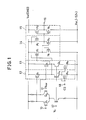
- FIG .1 illustrates a level converter, which includes a conventional emitter follower circuit.
- a differential circuit is made up of transistors Q1 and Q2.
- the transistor Q1 is supplied with a voltage signal through a terminal 10, and the transistor Q2 supplied with a reference voltage V REF through a terminal 11.
- Two output signals derived from the differential circuit pass through emitter follower circuits 12 and 13 including transistors Q3 and Q4, respectively, and are supplied to a flip-flop 14, which includes MOS transistors P1, P2, N1 and N2.
- An output signal derived from the flip-flop 14 passes through an inverter 15 including MOS transistors P3 and N3, and is output through a terminal 16.
- the flip-flop 14 has a function of converting the ECL (Emitter Coupled Logic) level of a supplied signal to the MOS level.
- the emitter follower circuits 11 and 13 include transistors Q5 and Q6, respectively, which function as constant-current sources, each of which is supplied to a fixed voltage V R through a terminal 17.
- N-channel MOS transistors N4 and N5 are current source resistors, and conduct when a chip select signal CS applied through a terminal 18 is held at a high (H) level, so that emitter follower circuits 12 and 13 are held in the active state.
- the MOS transistors N4 and N5 are cut off when the chip select signal CL is switched to a low (L) level, so that the emitter follower circuits 12 and 13 are switched to the inactive state.
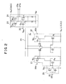
- FIG.2 illustrates a sense amplification circuit for a memory including a conventional emitter follower circuit.
- terminals 20a and 20b are connected to bit lines (not shown) which are paired.
- the voltages of the terminals 20a and 20b pass through emitter follower circuits 21 and 22 including transistors Q10 and Q11, respectively, and are then applied to a differential circuit made up of transistors Q12 and Q13.
- the collectors of the transistors Q12 and Q13 are coupled to corresponding current/voltage conversion circuits 25 and 26 through corresponding common lines 23 and 24, which are used in common with differential circuits associated with other bit lines.
- a fixed voltage V CNO is applied, through a terminal 30, to the base of transistors Q14 and Q15, which are included in the current/voltage conversion circuits 25 and 16, respectively.
- Collector currents of the transistors Q14 and Q15 are converted to corresponding voltages by the MOS transistors N12 and N13, respectively, which function as resistors.
- the output signals of the current/voltage conversion circuits 25 and 26 are supplied to a differential amplifier (not shown) of the next stage through terminals 27a and 27b, respectively.
- the N-channel MOS transistors N10 and N11 included in the emitter follower circuits 21 and 22 are current source resistors.
- the MOS transistors N10 and N11 conduct when a bit select signal BS supplied from a terminal 28 through an inverter is held at L level, whereby the emitter follower circuits 11 and 22 are held in the active state.
- the MOS transistors N10 and N11 are cut off when the bit select signal BS is held at H level, so that the emitter follower circuits 21 and 22 are held in the inactive state.
- FIG.1 when the emitter follower circuits 12 and 13 are switched to the inactive state, the potential of the emitter of each of the transistors Q3 and Q4 becomes unstable. Therefore, the flip-flop 14 becomes unstable, and the input signal of the inverter is unnecessarily inverted. It is noted that the circuit of FIG.1 is wasteful of current when the MOS transistors P1, P2, N1 and N2 included in the flip-flop 14 and the inverter 15 are inverted. The above leads to an increase of consumption power.
- the potential of emitter of each of the transistors Q10 and Q11 becomes unstable, when the emitter follower circuits 21 and 22 are switched to the inactive state.
- the emitter potentials of the transistors Q10 and Q11 decrease to the ground level (Vcc) as time goes. Therefore, it takes long for the emitter potential of each of the transistors Q10 and Q11 to become equal to the predetermined potential when the emitter follower circuits 21 and 22 is set to the active state again. The above prevents the sense amplifier from operating at high speeds.
- An object of the present invention is to provide an emitter follower circuit capable of reducing power consumption in the level converter circuit and enabling it to be possible to operate the sense amplification circuit at high speeds.
- the present invention relates to an emitter follower circuit including an emitter follower transistor, and a power source coupled to the emitter of the emitter follower transistor.
- the power source includes a MOS transistor, and the emitter follower circuit is switched between active and inactive states by switching the MOS transistor by a control signal.
- the present invention has the following essential features. That is, between the source and drain of the MOS transistor, there is provided current path means for providing a resistance considerably larger than a resistance of the MOS transistor provided during conducting, when the MOS transistor is at least cut off and for passing an extremely small current therethrough at that time.
- the extremely small current passes through the current path means during the time when the MOS transistor is OFF so that the emitter potential of the emitter follower transistor can be stabilized.
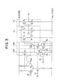
- FIG.3 is a circuit diagram of a level converter circuit in which an emitter follower circuit of an embodiment of the present invention is employed.
- Emitter follower circuits 12A and 13A correspond to emitter follower circuits 12 and 13, respectively.
- a resistor R1 is connected across the source and drain of the MOS transistor N4 provided in the emitter follower circuit 12A. Similarly, a resistor R1 is connected across the drain and source of the MOS transistor MS.
- the resistors R1 and R2 have resistances which are considerably larger than an ON resistance of each of the MOS transistors N4 and N5. It is preferable that each of the resistors R1 and R2 has a resistance as large as 10 times the ON resistance. Generally, the ON resistance of a MOS transistor is a few hundred ohms. Therefore, each of the resistors R1 and R2 is formed by a resistor having a resistance equal to or larger than a few kilo-ohms.
- a P-channel MOS transistor may be substituted for the resistor R1 as the current path means.
- the source and drain of the MOS transistor P4 are connected to the source and drain of the MOS transistor N4, respectively.
- the gate of the MOS transistor P4 is connected to the terminal 18.
- the ON resistance of the MOS transistor P4 is selected in the same way as the resistor R1. In the case of FIG. 4, an extremely small current passes through the MOS transistor P4, only when the MOS transistor N4 is cut off and thereby the emitter follower circuit 12A is held in the inactive state.
- resistor R2 may be replaced with a P-channel MOS transistor as described previously.
- FIG.5 illustrates a sense amplifier to which the present invention is applied.
- Emitter follower circuits 21A and 22A correspond to the aforementioned emitter follower circuits 21 and 22.
- a resistor R3 is connected across the drain and source of the MOS transistor N10 provided in the emitter follower circuit 21A, and a resistor R4 is connected across the drain and source of the MOS transistor N11.
- the resistances of the resistors R3 and R4 are set considerably large, compared with the MOS transistors N10 and N11. Thereby, even when the bit select signal held at H level and therefore the emitter follower circuits 21A and 22A are held in the inactive state, extremely small currents pass through the resistors R3 and R4. Therefore, the potentials of the emitters of the transistors Q10 and Q11 are fixed to levels which are lower by a fixed voltage than the potential of the terminals 20a and 20b, respectively. Thereby, it becomes possible to reduce a time it take for the emitter potential of each of the transistors Q10 and Q11 to become equal to the predetermined potential when the emitter follower circuits 21A and 22A are switched to the active state.
- the P-channel MOS transistor as shown in FIG .4 may be substituted for each of the resistors R3 and R4 as the current path means.
- the emitter follower circuit of the present invention As described above, according to the emitter follower circuit of the present invention, an extremely small current passes through the emitter follower circuit when held in the inactive state, and thereby emitter potential of the emitter follower transistor can be settled. As a result, it becomes possible to reduce the consumption power in the level converter circuit and operate the sense amplification circuit at high speeds. Consequently, the present invention is effective to practical use.
Landscapes
- Physics & Mathematics (AREA)
- Engineering & Computer Science (AREA)
- Computer Hardware Design (AREA)
- Computing Systems (AREA)
- General Engineering & Computer Science (AREA)
- Mathematical Physics (AREA)
- Logic Circuits (AREA)
- Amplifiers (AREA)
- Manipulation Of Pulses (AREA)
- Static Random-Access Memory (AREA)
Abstract
Applications Claiming Priority (2)
| Application Number | Priority Date | Filing Date | Title |
|---|---|---|---|
| JP233190/87 | 1987-09-17 | ||
| JP62233190A JPS6474823A (en) | 1987-09-17 | 1987-09-17 | Emitter follower circuit |
Publications (3)
| Publication Number | Publication Date |
|---|---|
| EP0333864A1 true EP0333864A1 (fr) | 1989-09-27 |
| EP0333864A4 EP0333864A4 (fr) | 1989-12-18 |
| EP0333864B1 EP0333864B1 (fr) | 1992-07-22 |
Family
ID=16951153
Family Applications (1)
| Application Number | Title | Priority Date | Filing Date |
|---|---|---|---|
| EP88907769A Expired EP0333864B1 (fr) | 1987-09-17 | 1988-09-13 | circuit emetteur-suiveur |
Country Status (5)
| Country | Link |
|---|---|
| US (1) | US4958094A (fr) |
| EP (1) | EP0333864B1 (fr) |
| JP (1) | JPS6474823A (fr) |
| DE (1) | DE3873071T2 (fr) |
| WO (1) | WO1989002677A1 (fr) |
Cited By (5)
| Publication number | Priority date | Publication date | Assignee | Title |
|---|---|---|---|---|
| EP0363189A3 (en) * | 1988-10-06 | 1990-08-16 | Nec Corporation | Three state emitter coupled logic circuit with a small amount of current consumption |
| EP0485291A3 (en) * | 1990-11-06 | 1992-08-19 | Fujitsu Limited | Level conversion circuit |
| EP0613247A2 (fr) * | 1993-01-08 | 1994-08-31 | DYNA LOGIC CORPORATION (a Californian Corporation) | Logique BICMOS reprogrammable |
| EP0429829B1 (fr) * | 1989-11-22 | 1997-04-09 | STMicroelectronics S.r.l. | Circuit comparateur électronique |
| EP1137185A1 (fr) * | 2000-03-24 | 2001-09-26 | SiGe Microsystems Inc. | Circuit hybride comprenant une source de courant commandée par un comparateur |
Families Citing this family (9)
| Publication number | Priority date | Publication date | Assignee | Title |
|---|---|---|---|---|
| JPH082019B2 (ja) * | 1989-09-13 | 1996-01-10 | 株式会社東芝 | レベル変換回路 |
| JP2547863B2 (ja) * | 1989-10-06 | 1996-10-23 | 東芝マイクロエレクトロニクス株式会社 | ソースカップルドfetロジック形出力回路 |
| JP2518068B2 (ja) * | 1989-11-17 | 1996-07-24 | 日本電気株式会社 | 電流切換回路 |
| US5216298A (en) * | 1989-12-14 | 1993-06-01 | Mitsubishi Denki Kabushiki Kaisha | ECL input buffer for BiCMOS |
| US5017812A (en) * | 1990-03-20 | 1991-05-21 | Integrated Device Technology, Inc. | Combined ECL-to-TTL translator and decoder |
| JP3001014B2 (ja) * | 1991-03-13 | 2000-01-17 | 富士通株式会社 | バイアス電圧発生回路 |
| US5315167A (en) * | 1992-04-09 | 1994-05-24 | International Business Machines Corporation | Voltage burn-in scheme for BICMOS circuits |
| JP2570185B2 (ja) * | 1994-07-08 | 1997-01-08 | 日本電気株式会社 | サンプルホールド回路 |
| JP3149759B2 (ja) * | 1995-11-17 | 2001-03-26 | 日本電気株式会社 | ラッチ回路 |
Family Cites Families (16)
| Publication number | Priority date | Publication date | Assignee | Title |
|---|---|---|---|---|
| JPS4953365A (fr) * | 1972-09-25 | 1974-05-23 | ||
| US4099070A (en) * | 1976-11-26 | 1978-07-04 | Motorola, Inc. | Sense-write circuit for random access memory |
| JPS5428707A (en) * | 1977-08-08 | 1979-03-03 | Tokyo Yogyo Kk | Container for molten metal for use in iron producing process |
| DE2740353C2 (de) * | 1977-09-07 | 1982-05-13 | Siemens AG, 1000 Berlin und 8000 München | ECL-kompatibler Registerbaustein mit bipolaren Speicherzellen |
| JPS5883434A (ja) * | 1981-11-13 | 1983-05-19 | Hitachi Ltd | 半導体集積回路装置 |
| JPS5912661A (ja) * | 1982-07-13 | 1984-01-23 | Fujitsu Ltd | 閾値可変型差動信号レシ−バ |
| US4604533A (en) * | 1982-12-28 | 1986-08-05 | Tokyo Shibaura Denki Kabushiki Kaisha | Sense amplifier |
| JPS60141019A (ja) * | 1983-12-28 | 1985-07-26 | Nec Corp | 論理回路 |
| JPS60176978A (ja) * | 1984-02-22 | 1985-09-11 | 株式会社イナックス | 高強度セメント製品の製法 |
| JPS6145491A (ja) * | 1984-08-10 | 1986-03-05 | Fujitsu Ltd | 半導体記憶装置 |
| JPS62159916A (ja) * | 1986-01-09 | 1987-07-15 | Toshiba Corp | レベル変換回路 |
| US4713560A (en) * | 1986-06-05 | 1987-12-15 | Fairchild Semiconductor Corporation | Switched impedance emitter coupled logic gate |
| JPS635617A (ja) * | 1986-06-25 | 1988-01-11 | Hitachi Ltd | 半導体回路 |
| US4868421A (en) * | 1987-02-24 | 1989-09-19 | Fairchild Semiconductor Corporation | Bimos circuit that provides low power dissipation and high transient drive capability |
| US4858183A (en) * | 1987-06-02 | 1989-08-15 | Texas Instruments Incorporated | ECL high speed semiconductor memory and method of accessing stored information therein |
| JPS6424628A (en) * | 1987-07-21 | 1989-01-26 | Fujitsu Ltd | Emitter coupled logic circuit |
-
1987
- 1987-09-17 JP JP62233190A patent/JPS6474823A/ja active Pending
-
1988
- 1988-09-13 EP EP88907769A patent/EP0333864B1/fr not_active Expired
- 1988-09-13 DE DE8888907769T patent/DE3873071T2/de not_active Expired - Lifetime
- 1988-09-13 US US07/391,605 patent/US4958094A/en not_active Expired - Lifetime
- 1988-09-13 WO PCT/JP1988/000923 patent/WO1989002677A1/fr not_active Ceased
Cited By (6)
| Publication number | Priority date | Publication date | Assignee | Title |
|---|---|---|---|---|
| EP0363189A3 (en) * | 1988-10-06 | 1990-08-16 | Nec Corporation | Three state emitter coupled logic circuit with a small amount of current consumption |
| EP0429829B1 (fr) * | 1989-11-22 | 1997-04-09 | STMicroelectronics S.r.l. | Circuit comparateur électronique |
| EP0485291A3 (en) * | 1990-11-06 | 1992-08-19 | Fujitsu Limited | Level conversion circuit |
| US5287019A (en) * | 1990-11-06 | 1994-02-15 | Fujitsu Limited | ECL to CMOS level conversion circuit |
| EP0613247A2 (fr) * | 1993-01-08 | 1994-08-31 | DYNA LOGIC CORPORATION (a Californian Corporation) | Logique BICMOS reprogrammable |
| EP1137185A1 (fr) * | 2000-03-24 | 2001-09-26 | SiGe Microsystems Inc. | Circuit hybride comprenant une source de courant commandée par un comparateur |
Also Published As
| Publication number | Publication date |
|---|---|
| US4958094A (en) | 1990-09-18 |
| WO1989002677A1 (fr) | 1989-03-23 |
| EP0333864B1 (fr) | 1992-07-22 |
| DE3873071D1 (de) | 1992-08-27 |
| DE3873071T2 (de) | 1992-12-03 |
| EP0333864A4 (fr) | 1989-12-18 |
| JPS6474823A (en) | 1989-03-20 |
Similar Documents
| Publication | Publication Date | Title |
|---|---|---|
| EP0333864B1 (fr) | circuit emetteur-suiveur | |
| EP0231062A1 (fr) | Circuit de conversion de niveau | |
| JPH029221A (ja) | Ecl―cmos変換器 | |
| US4607177A (en) | Circuit arrangement for conversion TTL logic signals to ECL logic signals | |
| JP3003625B2 (ja) | Cmlcmos変換回路 | |
| US5216298A (en) | ECL input buffer for BiCMOS | |
| US4639661A (en) | Power-down arrangement for an ECL circuit | |
| JPS6210920A (ja) | デイジタルマルチプレクサモジユ−ルおよびこのモジユ−ルを具えるマルチプレクサ | |
| EP0555075A2 (fr) | Convertisseur de niveau à basse consommation | |
| JP2743401B2 (ja) | Ecl回路 | |
| US5198704A (en) | Bi-CMOS output circuit with limited output voltage | |
| US5359553A (en) | Low power ECL/MOS level converting circuit and memory device and method of converting a signal level | |
| US4801825A (en) | Three level state logic circuit having improved high voltage to high output impedance transition | |
| US5287016A (en) | High-speed bipolar-field effect transistor (BI-FET) circuit | |
| US5083046A (en) | Source-coupled fet logic type output circuit | |
| KR920004343B1 (ko) | 인터페이스 회로 | |
| US6380794B1 (en) | Hybrid circuit having current source controlled by a comparator | |
| JP2754906B2 (ja) | 半導体集積回路 | |
| US5446400A (en) | GTL compatible BICMOS input stage | |
| JP2638016B2 (ja) | 半導体回路 | |
| JP2540928B2 (ja) | 論理回路 | |
| US5148060A (en) | Ecl input buffer for bicmos | |
| US5434517A (en) | ECL output buffer with a MOS transistor used for tristate enable | |
| US6014045A (en) | Minimal headroom, minimal area multi-terminal current steering circuits | |
| US5397935A (en) | Bias current supplying circuit |
Legal Events
| Date | Code | Title | Description |
|---|---|---|---|
| PUAI | Public reference made under article 153(3) epc to a published international application that has entered the european phase |
Free format text: ORIGINAL CODE: 0009012 |
|
| 17P | Request for examination filed |
Effective date: 19890605 |
|
| AK | Designated contracting states |
Kind code of ref document: A1 Designated state(s): DE FR GB |
|
| A4 | Supplementary search report drawn up and despatched |
Effective date: 19891218 |
|
| 17Q | First examination report despatched |
Effective date: 19911002 |
|
| GRAA | (expected) grant |
Free format text: ORIGINAL CODE: 0009210 |
|
| AK | Designated contracting states |
Kind code of ref document: B1 Designated state(s): DE FR GB |
|
| REF | Corresponds to: |
Ref document number: 3873071 Country of ref document: DE Date of ref document: 19920827 |
|
| ET | Fr: translation filed | ||
| PLBE | No opposition filed within time limit |
Free format text: ORIGINAL CODE: 0009261 |
|
| STAA | Information on the status of an ep patent application or granted ep patent |
Free format text: STATUS: NO OPPOSITION FILED WITHIN TIME LIMIT |
|
| 26N | No opposition filed | ||
| PGFP | Annual fee paid to national office [announced via postgrant information from national office to epo] |
Ref country code: GB Payment date: 19970904 Year of fee payment: 10 |
|
| PGFP | Annual fee paid to national office [announced via postgrant information from national office to epo] |
Ref country code: FR Payment date: 19970909 Year of fee payment: 10 |
|
| PGFP | Annual fee paid to national office [announced via postgrant information from national office to epo] |
Ref country code: DE Payment date: 19970919 Year of fee payment: 10 |
|
| PG25 | Lapsed in a contracting state [announced via postgrant information from national office to epo] |
Ref country code: GB Free format text: LAPSE BECAUSE OF NON-PAYMENT OF DUE FEES Effective date: 19980913 |
|
| GBPC | Gb: european patent ceased through non-payment of renewal fee |
Effective date: 19980913 |
|
| PG25 | Lapsed in a contracting state [announced via postgrant information from national office to epo] |
Ref country code: FR Free format text: LAPSE BECAUSE OF NON-PAYMENT OF DUE FEES Effective date: 19990531 |
|
| PG25 | Lapsed in a contracting state [announced via postgrant information from national office to epo] |
Ref country code: DE Free format text: LAPSE BECAUSE OF NON-PAYMENT OF DUE FEES Effective date: 19990701 |
|
| REG | Reference to a national code |
Ref country code: FR Ref legal event code: ST |