EP0337202B1 - Mémoire RAM statique avec un détecteur de changement d'adresse - Google Patents
Mémoire RAM statique avec un détecteur de changement d'adresse Download PDFInfo
- Publication number
- EP0337202B1 EP0337202B1 EP89105628A EP89105628A EP0337202B1 EP 0337202 B1 EP0337202 B1 EP 0337202B1 EP 89105628 A EP89105628 A EP 89105628A EP 89105628 A EP89105628 A EP 89105628A EP 0337202 B1 EP0337202 B1 EP 0337202B1
- Authority
- EP
- European Patent Office
- Prior art keywords
- gate
- mosfet
- current path
- output terminal
- output
- Prior art date
- Legal status (The legal status is an assumption and is not a legal conclusion. Google has not performed a legal analysis and makes no representation as to the accuracy of the status listed.)
- Expired - Lifetime
Links
- 230000007704 transition Effects 0.000 title claims description 57
- 230000003068 static effect Effects 0.000 title claims description 17
- 239000011159 matrix material Substances 0.000 claims description 3
- 230000003213 activating effect Effects 0.000 claims 1
- 238000010586 diagram Methods 0.000 description 8
- 230000007257 malfunction Effects 0.000 description 3
- 208000032368 Device malfunction Diseases 0.000 description 1
- 230000009286 beneficial effect Effects 0.000 description 1
- 230000001934 delay Effects 0.000 description 1
- 238000000034 method Methods 0.000 description 1
Images



Classifications
-
- G—PHYSICS
- G11—INFORMATION STORAGE
- G11C—STATIC STORES
- G11C8/00—Arrangements for selecting an address in a digital store
-
- G—PHYSICS
- G11—INFORMATION STORAGE
- G11C—STATIC STORES
- G11C8/00—Arrangements for selecting an address in a digital store
- G11C8/18—Address timing or clocking circuits; Address control signal generation or management, e.g. for row address strobe [RAS] or column address strobe [CAS] signals
-
- G—PHYSICS
- G11—INFORMATION STORAGE
- G11C—STATIC STORES
- G11C11/00—Digital stores characterised by the use of particular electric or magnetic storage elements; Storage elements therefor
- G11C11/21—Digital stores characterised by the use of particular electric or magnetic storage elements; Storage elements therefor using electric elements
- G11C11/34—Digital stores characterised by the use of particular electric or magnetic storage elements; Storage elements therefor using electric elements using semiconductor devices
- G11C11/40—Digital stores characterised by the use of particular electric or magnetic storage elements; Storage elements therefor using electric elements using semiconductor devices using transistors
- G11C11/41—Digital stores characterised by the use of particular electric or magnetic storage elements; Storage elements therefor using electric elements using semiconductor devices using transistors forming static cells with positive feedback, i.e. cells not needing refreshing or charge regeneration, e.g. bistable multivibrator or Schmitt trigger
- G11C11/413—Auxiliary circuits, e.g. for addressing, decoding, driving, writing, sensing, timing or power reduction
- G11C11/417—Auxiliary circuits, e.g. for addressing, decoding, driving, writing, sensing, timing or power reduction for memory cells of the field-effect type
- G11C11/418—Address circuits
-
- G—PHYSICS
- G11—INFORMATION STORAGE
- G11C—STATIC STORES
- G11C7/00—Arrangements for writing information into, or reading information out from, a digital store
- G11C7/06—Sense amplifiers; Associated circuits, e.g. timing or triggering circuits
- G11C7/062—Differential amplifiers of non-latching type, e.g. comparators, long-tailed pairs
-
- G—PHYSICS
- G11—INFORMATION STORAGE
- G11C—STATIC STORES
- G11C7/00—Arrangements for writing information into, or reading information out from, a digital store
- G11C7/12—Bit line control circuits, e.g. drivers, boosters, pull-up circuits, pull-down circuits, precharging circuits, equalising circuits, for bit lines
Definitions
- the present invention relates to a static random access memory (SRAM) comprising: a memory cell array containing a plurality of static memory cells for storing data arrayed in a matrix fashion; word lines for selecting rows of the memory cells in said memory cell array, said word lines being arranged along the rows of said memory cell array; bit line pairs arranged along the columns of the memory cells in said memory cell array, said bit line pairs each corresponding to one column of said memory cells to transfer data to and from one of the memory cells of the selected column; address input means for receiving an address signal to select one of said memory cells of said memory cell array; row decoder means for decoding a row address signal supplied from said address input means and for selectively driving said word lines; column decoder means for decoding a column address signal supplied from said address input means to select one of said bit line pairs; address transition detector means for detecting a transition of an address signal supplied from said address input means, to generate an address transition detect signal; bit line initialize means for initializing the potential of each said bit line pair to a predetermined potential,
- Such a memory is disclosed in "Two 13-ns 64K CMOS SRAM's with Very Low Active Power and Improved Asynchronous Circuit Techniques", by Flannagan et al, published in IEEE Journal of Solid-State Circuits, vol. SC-21, No.5, Oct.1986., pp 692-703.
- the SRAM is also described in, for example, IEEE Journal of Solid-State Circuits, Vol. SC-19, No. 5, October 1984, "A LOW POWER 46ns 256kbit CMOS STATIC RAM WITH DYNAMIC DOUBLE WORD LINE", Sakurai et al., and 1987 IEEE Journal of Solid-State Circuits Conference DIGEST OF TECHNICAL PAPERS "A 25ns 1Mb CMOS SRAMs" Ohtani et al.
- the SRAMS discussed in these papers contain ATDs.
- the output stage of a data output circuit is provided with a pull-up transistor for pulling up a potential at the data output terminal, and a pull-down transitor for pulling down the potential at that terminal.
- a pull-up transistor for pulling up a potential at the data output terminal
- a pull-down transitor for pulling down the potential at that terminal.
- An object of the present invention is to provide a static random access memory capable of minimizing the read time delay and the malfunction, which arise from the power noise.
- the memory initially defined is characterized by: clock signal generator means for generating a clock signal a predetermined period of time elapsing from generation of said address transition detect signal in a read mode, said clock signal generator means being coupled for reception of said address transition detect signal from said address transition detector means; said sense amplifier means being initialized by an address transition detect signal generated by said address transition detector means and rendered active by removal of said detect signal during a period of time that said sense amplifier means receives said clock signal from said clock signal generator means; said data output means outputting the amplified signal from said sense amplifier means during a period that said clock signal is being generated, and holding the amplified signal after generation of said clock signal ceases; a data output detector means being provided for detecting whether said data output means is in a data outputting state by determining data output from said sense amplifier means to said data output means; and a logic means being provided for logically summing the output signal of said clock signal generator means and the output signal of said data output detector means and controlling said sense amplifier means and said data output means on the
- the output terminal of the data output circuit in a read mode, is placed in a high impedance state during a period from the inputting of an address signal till the outputting of the data read out of a memory cell specified by the address signal. Therefore, when the data currently read out is different from the data previously read out, no through-current flows between a power source and a ground potential.
- the SRAM is less susceptible to read time delay and malfunction, which are problems of the prior art.
- Fig. 1 is a block diagram showing an arrangement of an SRAM.
- An address input terminal 1 to which an address signal Add is applied is connected to the input terminal of an address input circuit 2.
- the output terminal of the address input circuit 2 is connected to the input terminal of a row decoder 3.
- the row decoder 3 decodes a row address signal derived from the address input circuit 2.
- Word lines 4 are connected to the output terminals of the row decoder 3.
- the word lines 4 are selectively driven by an output signal of the row decoder 3.
- Paired bit lines 5 and 5 are disposed orthogonal to the word lines 4.
- Each pair of bit lines 5 and 5 is coupled at first end to a bit line initializing circuit 6, which is provided in association with the bit line pair.
- Each bit line initializing circuit 6 is for initializing a potential of the paired bit lines 5 and 5 to a predetermined potential.
- Static memory cells 7 are located at the cross-points of the word lines 4 and the bit line pairs 5 and 5 , respectively, forming a matrix array MA of the memory cells.
- the input terminal of a column decoder 8 is connected to the output terminal of the address input circuit 2.
- the column decoder 8 decodes a column address signal derived from the address input circuit 2.
- Each column selector 9 is connected to a second terminal of the bit line pair 5 and 5 , which is provided in association with the column selector 9.
- the column selector 9 is driven by a column select signal supplied through an output line 22 of the column decoder 8.
- a sense amplifier 10 is connected at the input terminal to the output terminal of the column selector 9, through a pair of sense amplifier input lines 25 and 25 .
- the sense amplifier 10 amplifies the data read out from a memory cell which is selected by the cooperation of the row decoder 3 and the column decoder 8.
- a data output circuit 11 is connected to the output terminals of the sense amplifier 10, through a pair of sense amplifier output lines 26 and 26 .
- a data output terminal 12 is connected to the output terminal of the sense amplifier 10.
- the data, which is read out of the memory cell 7 and amplified by the sense amplifier 10 is applied through the data output circuit 11 to the data output terminal 12 and is outputted to exterior.
- the input terminal of an address transition detector 13 is connected to the address input circuit 2.
- the address transition detector 13 detects a transition of an address signal inputted to the address input circuit 2, and produces an address transition detect signal SATD.
- the address transition detect signal SATD is supplied through an output line 21 of the address transistor detector 13 to the bit line initializing circuits 6, through an output line 24 to the sense amplifier 10, and through an output line 27 to a clock signal generator 14.
- the clock signal generator 14 receives the address transition detect signal SATD from the address transition detector 13, and produces a clock signal ⁇ S that is effective in level for a fixed period.
- the clock signal ⁇ S is applied through a clock signal line 23 to the sense amplifier 10 and the data output circuit 11, so that those circuits are rendered active during the fixed period.
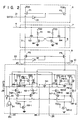
- Fig. 2 shows the details of an arrangement of a part of the SRAM circuit of Fig. 1, which contains the bit line initializing circuit 6, memory cell 7, row selector 9, and sense amplifier 10 which are provided in connection with one column of the memory cell array MA.
- the bit line initializing circuit 6 is made up of a pair of p-channel MOSFETs P1 and P2, and an inverter 31.
- the source of the MOSFET P1 is connected to a power source V DD , and the drain thereof to the bit line 5.
- the source of the MOSFET P2 is connected to the power source V DD , and the drain thereof to the bit line 5 .
- the gates of the MOSFETs P1 and P2 are connected together, and a connection point of those gates is connected to the output terminal of the inverter 31.
- the input terminal of the inverter 31 is connected to the output line 21 of the address transition detector 13. With this connection, the address transition detector 13 supplies the address transition detect signal SATD to the inverter 31.
- bit line initializing circuit 6 when the address transition detect signal SATD goes high, the MOSFETs P1 and P2 are both turned on to initialize the bit line pair 5 and 5 and set it at a level of a power source voltage V DD .
- the memory cell 7 is made up of resistors R1 and R2 as high resistance loads, drive MOSFETs N1 and N2, and transfer MOSFETs N3 and N4.
- the resistor R1 is connected at one end to the power source V DD and at the other end to the drain of the drive MOSFET N1.
- the resistor R2 is connected at one end to the power source V DD and at the other end to the drain of the drive MOSFET N2.
- the gate of the drive MOSFET N1 is connected to the drain of the drive MOSFET N2 and the source thereof to a ground point.
- the gate of the drive MOSFET N2 is connected to the drain of the drive MOSFET N1 and the source thereof to a ground point.
- a current path between the source and drain of the transfer MOSFET N3 is inserted between the bit line 5 and the drain of the drive MOSFET N1.
- a current path between the source and drain of the transfer MOSFET N4 is inserted between the bit line 5 and the drain of the drive MOSFET N2.
- the word line 4 is connected to the gates of the MOSFETs N3 and N4.
- one of the drive MOSFETs N1 and N2 is in an on state and the other in an off state in accordance with the content of the stored data.
- the transfer MOSFETs N3 and N4 are both turned on. A potential of the bit line connected to the drive MOSFET being in an on state drops, while a potential of the bit line connected to the drive MOSFET being in an off state is maintained in V DD level.
- the column selector 9 is made up of p-channel MOSFETs P3 and P4, and an inverter 32.
- the drain of the MOSFET P3 is connected to the bit line 5, and the drain of the MOSFET P4 to the bit line 5 .
- the source of the MOSFET P3 is connected to one end of a sense amplifier input line 25, and the source of the MOSFET P4 is connected to one end of a sense amplifier input line 25 .
- the gates of the MOSFETs P3 and P4 are connected together, and a connection point of these gates is connected to the output terminal of the inverter 32.
- the input terminal of the inverter 32 is connected to an output line 22 of the column decoder 8, and supplied with a column select signal from the decoder 8.
- the sense amplifier 10 is made up of input MOSFETs of n-channel N5-1, N6-1, N5-2, and N6-2, control MOSFETs of n-channel N7-1, N8-1, N7-2 and N8-2, current restricting MOSFETs of n-channel N9-1 and N9-2, potential equalizing MOSFETs of n-channel N10-1, N10-2, and N11, load MOSFETs of p-channel P5-1, P6-1, P5-2, and P6-2, p-channel MOSFETs for sense amplifier initialization P7-1, P8-1, P7-2 and P8-2, an inverter 33, and an AND gate 34.
- the other end of the sense amplifier input line 25 is connected to the gates of MOSFETs N6-1 and N5-2.
- the current paths of the MOSFETs P8-1 and P6-1 are connected in parallel between the drain of the MOSFET N6-1 and the power source V DD .
- the other end of the sense amplifier input line 25 is connected to the gates of MOSFETs P7-1 and P5-1.
- the current paths of the MOSFETs P7-1 and P5-1 are connected in parallel between the drain of the MOSFET N5-1 and the power source V DD .
- the gates of the MOSFETs P8-1 and P7-1 are connected to the output terminal of the AND gate 34.
- the gates of the MOSFETs P6-1 and P5-1 are connected together, and a connection point of them is further connected to the drain of the MOSFET P6-1.
- a current path between the source and drain of the MOSFET N10-1 is inserted between the drain of the MOSFET P6-1 and the drain of the MOSFET P5-1.
- the gate of the MOSFET N10-1 is connected to the output line 24 of the address transition detector 13.
- the source of the MOSFET N6-1 is connected to the drain of the MOSFET N8-1, and the source of the MOSFET N5-1 is connected to the drain of the MOSFET N7-1.
- the sources of the MOSFETs N8-1 and N7-1 are connected together and the gates of them are connected to the output terminal of the AND gate 34.
- One of the input terminals of the AND gate 34 is connected to a clock signal line 23, and the other input terminal thereof is connected to the output terminal of the inverter 33.
- the input terminal of the inverter 33 is connected to the output line 24.
- a source-drain current path of the MOSFET N9-1 is connected to a ground point and a node where the sources of the MOSFETs N8-1 and N7-1 are interconnected.
- the gate of the MOSFET N9-1 is connected to the power source V DD .
- the current paths of the MOSFETs P7-2 and P5-2 are connected in parallel between the drain of the MOSFET N5-2 and the power source V DD .
- the current paths of the MOSFETs P8-2 and P6-2 are connected in parallel between the drain of the MOSFET N6-2 and the power source V DD .
- the gates of the MOSFETs P7-2 and P8-2 are connected to the output terminal of the AND gate 34.
- the gates of the MOSFETs P5-2 and P6-2 are interconnected and then to the drain of the MOSFET P6-2.
- the current path between the source and drain of the MOSFET N10-2 is connected between the drain of the MOSFET P5-2 and the drain of the MOSFET P6-2.
- the gate of the MOSFET N10-2 is connected to the output line 24 of the address transition detector 13.
- the source of the MOSFET N5-2 is coupled with the drain of the MOSFET N7-2
- the source of the MOSFET N6-2 is coupled with the drain of the MOSFET N8-2.
- the sources of the MOSFETs N7-2 and N8-2 are interconnected and the gates of them is connected to the output terminal of the AND gate 34.
- a source-drain current path of the MOSFET N9-2 is connected between a ground point and a connection point interconnecting the sources of the MOSFETs N7-2 and N8-2.
- the gate of the MOSFET N9-2 is connected to the power source V DD .
- a source-drain current path of the MOSFET N11 is inserted between the drains of the MOSFETs N5-1 and N5-2.
- the gate of the MOSFET N11 is connected to the output line 24.
- the drain of the MOSFET N5-1 is connected to one end of the sense amplifier output line 26, and the drain of the MOSFET N5-2 is connected to one end of the sense amplifier output line 26 .
- the sense amplifier thus arranged will operate in the following way.
- a transition of an address signal Add is detected by the address transition detector 13, so that an address transition detect signal SATD from the detector goes high.
- the signal SATD renders a clock signal ⁇ S produced from the clock signal generator 14 high in level.
- the MOSFETs N10-1, N10-2, N11, P8-1, P7-1, P7-2 and P8-2 are all turned on, while the MOSFETs N8-1, N7-1, N7-2, and N8-2 are all turned off. Under this condition, the potentials at the output node of the sense amplifier 10 and the sense amplifier output line pair 26 and 26 are initialized and set at a potential level of the power source voltage V DD .
- the address transition detect signal SATD goes low, and the clock signal ⁇ S maintains a high level. Under this condition, the MOSFETs N10-1, N10-2, N11, P8-1, P7-1, P7-2 and P8-2 are all turned off, while the MOSFETs N8-1, N7-1, N7-2, and N8-2 are all turned on. Then, the sense amplifier 10 becomes active, and amplifies a potential difference between paired input lines 25 and 25 for the sense amplifier.
- the clock signal ⁇ S goes low, fhe MOSFETs P8-1, P7-1, P7-2, and P8-2 are all turned on, and the MOSFETs N8-1, N7-1, N7-2, and N8-2 are all turned off. Accordingly, the sense amplifier 10 becomes inactive.
- the data output circuit 11 is made up of 2-input NOR gates 35 to 38, 40, and 41, inverters 39 and 42, a pull-up MOSFET P9 of p-channel, and a pull-down MOSFET N12 of n-channel.
- the 2-input NOR gates 35 to 38, 40, and 41, and the inverters 39 and 42 make up a master slave flip-flop.
- the MOSFETs P9 and N12 are turned on and off by the flip-flop.
- One of the input terminals of the NOR gate 35 is connected to the other end of the sense amplifier output line 26 , and one of the input terminals of the NOR gate 36 is connected to the other end of the sense amplifier output line 26.
- the other input terminal of the NOR gate 35 is connected to the output terminal of the NOR gate 36, and the other input terminal of the NOR gate 36 is connected to the output terminal of the NOR gate 35.
- the output terminal of the NOR gate 35 is connected to the one of the input terminals of the NOR gate 37, and the output terminal of the NOR gate 36 is connected to one of the input terminals of the NOR gate 38.
- the other input terminals of the NOR gates 37 and 38 are connected to the output terminal of the inverter 39.
- the input terminal of the inverter 39 is connected to the output line 23 of the address transition detector 13.
- One of the input terminals of the NOR gate 40 is connected to the output terminal of the NOR gate 37, and one of the input terminals of the NOR gate 41 is connected to the output terminal of the NOR gate 38.
- the output terminal of the NOR gate 41 is connected to the other input terminal of the NOR gate 40, and the output terminal of the NOR gate 40 is connected to the other input terminal of the NOR gate 41.
- the output terminal of the NOR gate 40 is connected to the input terminal of the inverter 42.
- the output terminal inverter 42 is connected to the gate of the MOSFET P9.
- the source of the MOSFET P9 is connected to the power source V DD , and the drain of it is connected to the data output terminal 12 and the drain of the MOSFET N12.
- the output terminal of the NOR gate 41 is connected to the gate of the MOSFET N12 whose source is grounded.
- MOSFETs P9 and N12 are both turned off.
- one of the MOSFETs is turned on, while the other is turned off in accordance with the potentials of the sense amplifier output lines 26 and 26 .
- the sense amplifier 10 is initialized and the sense amplifier output lines 26 and 26 become high. Accordingly, the output signals of the NOR gates 35 and 36 go low in level. Since the clock signal ⁇ S is high, the two input terminals of each NOR gate 37 and 38 are set in a low level.
- the output signals of the NOR gates 37 and 38 go high, so that the output signals of the NOR gates 40 and 41 also go high.
- the MOSFETs P9 and N12 are both turned off, and in turn the data output terminal 12 has a high impedance.
- the clock signal ⁇ S goes low (at this time the sense amplifier output line pair 26 and 26 is placed such that one of them is set in a high level and the other in a low level in accordance with the data read out of the selected memory cell)
- one of the MOSFETs is turned on and the other is turned off in accordance with the potentials of the output lines 26 and 26 .
- the result is that a high or low signal, which depends on the read data, is derived from the data output terminal 12.
- An address signal Add is supplied to the address input circuit 2 through the address input terminal 1.
- a row address signal contained in the address signal Add is applied to the row decoder 3, and a column address signal also contained in the same is applied to the column decorder 8.
- the address transition detector 13 detects a transition of the address signal Add, and produces an address transition detect signal SATD.
- SATD is supplied to the bit line initializing circuits 6, to initialize both the paired bit lines 5 and 5 and set them in the level of the power soruce voltage V DD .
- the row decoder 3 decodes a row address to select a specific word line 4.
- the memory cells 7 coupled with the selected word line 4 are all selected.
- a potential difference is caused between the paired bit lines 5 and 5 coupled with these memory cells 7.
- the column decoder 8 decodes a column address, and selects one column selector 9.
- the potential difference between the paired bit lines 5 and 5 of the selected column selector 9 is transferred to the sense amplifier 10.
- the address transition detect signal SATD drives the clock signal generator 14 which in turn generates a clock signal during a fixed period of time.
- the output line pair 26 and 26 of the sense amplifier 10 is initialized and set at the power source voltage V DD level. Thereafter, during a high level period of the clock signal ⁇ S, the active state of the sense amplifier 10 continues. Under this condition, the potential difference between the paired bit lines 5 and 5 , and the potential difference is supplied to the data output circuit 11.
- the output line pair 26 and 26 for the sense amplifier 10 is initialized to the V DD level, so that the data output terminal 12 exhibits a high impedance. Then, after the sense amplifier 10 operates, it outputs the data. After a predetermined period of time, the clock signal ⁇ S is returned to low, to render the sense amplifier 10 inactive. The data output circuit 11 continues the outputting of data Dout via the data output terminal 12.
- the MOSFETs P9 and N12 in the data output circuit 11 are both in an off state.
- the output terminal of the data output circuit 11 (data output terminal 12) is kept high in impedance. Therefore, even when the present data is different from the data previously read out, no through current flows between the power source V DD and a ground point. Consequently, the SRAM can minimize the read time delay and malfunction problem due to the power noise.
- Fig. 4 there is shown another configuration of the data output circuit 11, which is available for the SRAM of Fig. 1.
- the data output circuit 11 is composed of 2-input NAND gates 43 to 46, inverter 47, pull-up MOSFET of p-channel P9, and pull-down MOSFET of n-channel N12.
- the present circuit configuration like the Fig. 3 circuit, constitutes a master slave flip-flop.
- One of the input terminals of the NAND gate 43 is connected to the other end of the sense amplifier output line 26
- one of the input terminals of the NAND gate 44 is connected to the other end of the sense amplifier output line 26.
- the other input terminals of the NAND gates 43 and 44 are coupled with the output line 23 of the address transition detector 13.
- One of the input terminals of the NAND gate 45 is connected to the output terminal of the NAND gate 43, and one of the input terminals of the NAND gate 46 is connected to the output terminal of the NAND gate 44.
- the output terminal of the NAND gate 46 is connected to the other input terminal of the NAND gate 45, and the output terminal of the NAND gate 45 is connected to the other input terminal of the NAND gate 46.
- the output terminal of the NAND gate 45 is connected to the gate of the MOSFET P9.
- the source of the MOSFET P9 is connected to the power source V DD , and its drain is connected to the data output terminal 12 and the drain of the MOSFET N12.
- the output terminal of the NAND gate 46 is connected to the input terminal of the inverter 47, and the output terminal of this inverter is connected to the gate of the MOSFET N12 whose source is grounded.
- the above configuration of the data output circuit 11 has a similar logic operation to that of the Fig. 3 configuration.
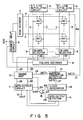
- Fig. 5 shows a circuit configuration of an SRAM according to an embodiment of the present invention.
- the Fig. 5 configuration improves over the Fig. 1 circuit in that a power dissipation is reduced in a read mode, and a read operation is more reliable.
- a data output circuit 11 is connected to the input terminal of a data output detector 15.
- An output line 28 of the data output detector 15 is connected to one of the input terminals of an OR gate 16.
- the other input terminal of the OR gate 16 is connected to a clock signal line 23 also coupled with the output terminal of a clock signal generator 14.
- a signal line 29 coupled with the output terminal of the OR gate 16 is connected to a sense amplifier 10 and a data output circuit 11.
- a circuit configuration of a part of the SRAM of Fig. 5, which contains a bit line initializing circuit 6, memory cell 7, column selector 9, and sense amplifier 10 which are provided in connection with one column line of an memory cell array MA, is the same as the Fig. 2 configuration.
- Fig. 6 shows the details of the data output circuit 11 and the data output detector 15 in the Fig. 5 circuit.
- a configuration of the circuit 11 is the same as that of the Fig. 3 circuit.
- the data output detector 15 consists of a 2-input NOR gate 48.
- the output terminal of the NOR gate 40 is connected to one of the input terminals of the NOR gate 48, while the output terminal of the NOR gate 41 to the other input terminal.
- the output terminal of the NOR gate 48 is connected to the output line 28.
- Figs. 5 and 6 An operation of the circuit illustrated in Figs. 5 and 6 will be described.
- Fig. 5 circuit an operation that after an address signal Add is inputted, the data from a selected memory cell 7 is supplied to the data output circuit 11 and is derived from the output terminal 12, is substantially the same as that of the Fig. 1 circuit.
- the SRAM of the second embodiment is different from the Fig. 1 circuit of the first embodiment in that a signal ⁇ SO as a logical sum of an output signal of the data output detector 15 and a clock signal ⁇ S from the clock signal generator 14 is used for controlling the sense amplifier 10 and the data output circuit 11. So long as the data output detector 15 detects the data outputting, if the clock signal ⁇ S goes low, the sense amplifier 10 and the data output circuit 11 are continuously active.
- a high level period of the clock signal ⁇ S is preset, as recalled. Therefore, a drive force by the memory cell 7 for the bit line pair 5 and 5 is weak.
- the clock signal ⁇ S may go low before the read operation ends. In such a case, the read operation is imperfect.
- the Fig. 5 circuit can successfully cope with such a situation.
- the output signal of the data output detector 15 continuously activates the sense amplifier 10 and the data output circuit 11.
- the read operation will be normally performed even when the drive.force by the memory cell 7 for the bit line pair 5 and 5 is weak. Additionally, an appropriate adjustment of a time length of generating the clock signal ⁇ S may reduce a power dissipation when the drive force of the memory cell 7. Specifically, the clock signal ⁇ S is pulsed from a high level to a low level immediately after the signal ⁇ S goes high to activate the sense amplifier 10 and the data output circuit 11, and the data output detector 15 produces a signal to activate the sense amplifier 10 and the data output circuit 11. If so pulsed, the memory cell 7 forcibly drives the bit line pair 5 and 5 . When the data is quickly applied through the sense amplifier to the data output circuit 11, the output signal of the data output detector 15 goes low immediately. Accordingly, the sense amplifier 10 and the data output circuit 11 are quickly rendered inactive, reducing a power dissipation by the sense amplifier 10 and the data output circuit 11.
- the read mode in a read mode, after the reading out data from the memory cell is detected, the read mode is terminated. Accordingly, the read operation is more reliable with a lessened power dissipation.
- FIG. 7 Another circuit configuration containing the data output circuit 11 and the data output detector 15 is shown in Fig. 7.
- the data output circuit 11 has the same configuration as that of the Fig. 4 circuit.
- the data output detector 15 is made up of a 2-input AND gate 49.
- the output terminal of a NAND gate 45 is connected to one of the input terminals of the AND gate 49, and the output terminal of a NAND gate 46 is connected to the other input terminal.
- the output terminal of the AND gate 49 is connected to the output line 28.
- the Fig. 7 circuit has substantially the same logical operation and the beneficial effects as the Fig. 6 circuit.
Landscapes
- Engineering & Computer Science (AREA)
- Microelectronics & Electronic Packaging (AREA)
- Computer Hardware Design (AREA)
- Static Random-Access Memory (AREA)
- Dram (AREA)
Claims (10)
- Mémoire à accès sélectif statique, comprenant :
un réseau de cellules de mémoire (MA) contenant une pluralité de cellules de mémoire statique (7) pour mémoriser des données, disposées en matrice ; des fils de mot (4) pour sélectionner des lignes des cellules de mémoire (7) dans ladite matrice de cellules de mémoire (MA), lesdits fils de mot (4) étant disposés le long des lignes de ladite matrice de cellules de mémoire (MA) ; des paires de fils de bit (5,5 ) disposées le long des colonnes des cellules de mémoire (7) dans ladite matrice de cellules de mémoire (MA), lesdites paires de fils de Vit (5,5 ) correspondant chacune à une colonne desdites cellules de mémoire pour transférer des données vers les et à partir des cellules de mémoire de la colonne sélectionnée ; un moyen d'entrée d'adresse (1,2) pour recevoir un signal d'adresse (Add) afin de sélectionner une desdites cellules de mémoire (7) de ladite matrice de cellules de mémoire (MA) ; un moyen décodeur de ligne (3) pour décoder un signal d'adresse de ligne fourni par ledit moyen d'entrée d'adresse (1 et 2) et pour commander sélectivement lesdits fils de mot (4) ; un moyen décodeur de colonne (8 et 9) pour décoder un signal d'adresse de colonne fourni par ledit moyen d'entrée d'adresse (1 et 2) afin de sélectionner une desdites paires de fils de bit (5,5 ) ; un moyen détecteur de changement d'adresse (13) pour détecter une transition d'un signal d'adresse (Add) fourni par ledit moyen d'entrée d'adresse (1,2), afin d'engendrer un signal de détection de changement d'adresse (SATD) ; un moyen d'initialisation de fil de bit (6) pour initialiser le potentiel de chaque dite paire de fils de bit (5,5 ) à un potentiel prédéterminé, ledit moyen d'initialisation de fil de bit (6) étant sous la commande d'un signal de détection de changement d'adresse (SATD) sorti par ledit moyen détecteur de changement d'adresse (13), quand une transition dudit signal d'adresse (Add) est détectée ; un moyen amplificateur de détection (10) pour amplifier la donnée telle que lue dans une cellule de mémoire sélectionnée (7) sur ladite paire de fils de bit (5,5 ) associée à ladite cellule de mémoire sélectionnée (7) ; et un moyen de sortie de données (11 et 12) pour sortir un signal (Dout) correspondant à la donnée telle que lue dans ladite cellule de mémoire (7) et sortie par ledit moyen amplificateur de détection (10), caractérisée par :
un moyen générateur de signaux d'horloge (14) pour engendrer un signal d'horloge (φs), une période de temps prédéterminée s'écoulant à partir de la génération dudit signal de détection de changement d'adresse (SATD) dans un mode de lecture, ledit moyen générateur de signaux d'horloge (14) étant couplé pour la réception dudit signal de détection de changement d'adresse (SATD) dudit moyen détecteur de changement d'adresse (13) ;
ledit moyen amplificateur de détection (10) étant initialisé par un signal de détection de changement d'adresse (SATD) engendré par ledit moyen détecteur de changement d'adresse (13) et rendu actif par la suppression dudit signal de détection (SATD) pendant une période de temps où ledit moyen amplificateur de détection (10) reçoit ledit signal d'horloge (φS) dudit moyen générateur de signaux d'horloge (14) ;
ledit moyen de sortie de données (11 et 12) sortant le signal amplifié dudit moyen amplificateur de détection (10) pendant une période où ledit signal d'horloge (φS) est engendré, et maintenant le signal amplifié après que la génération dudit signal d'horloge (φS) a cessé ;
un moyen détecteur de sortie de données (15) étant fourni pour détecter si ledit moyen de sortie de données (11) est dans un état de sortie des données en déterminant la sortie de données dudit moyen amplificateur de détection (10) vers ledit moyen de sortie de données (11) ; et,
un moyen logique (16) étant fourni pour faire la somme logique du signal de sortie (φS) dudit moyen générateur de signaux d'horloge (14) et du signal de sortie dudit moyen détecteur de sortie de données (15) et commander ledit moyen amplificateur de détection (10) et ledit moyen de sortie de données (11) selon la somme logique obtenue. - Mémoire à accès sélectif statique selon la revendication 1, caractérisée en ce que ledit moyen amplificateur de détection (10) inclut un moyen amplificateur différentiel (N6-1, N5-1, N9-1, P6-1, P5-1, N6-2, N5-2, N9-2, P6-2, P5-2) pour l'amplification différentielle des potentiels desdits fils de bit associés par paires (5,
5 ), un moyen de charge (N10-1, N10-2, N12) pour charger des noeuds de sortie (26,26 ) dudit moyen amplificateur différentiel (N6-1, N5-1, N9-1, P6-1, P5-1, N6-2, N5-2, N9-2, P6-2, P5-2) conformément à un moyen détecteur de changement d'adresse (13), et un moyen de commande (N8-1, N7-1, P8-1, P7-1, N8-2, N7-2, P8-2, P7-2) pour rendre actif ledit moyen amplificateur différentiel (N6-1, N5-1, N9-1, P6-1, P5-1, N6-2, N5-2, N9-2, P6-2, P5-2) quand le signal de détection de changement d'adresse est absent et un signal d'horloge (φS) est reçu dudit moyen générateur de signaux d'horloge (14), et pour rendre inactif ledit moyen amplificateur différentiel (N6-1, N5-1, N9-1, P6-1, P5-1, N6-2, N5-2, N9-2, P6-2, P5-2) quand ledit signal d'horloge (φS) se termine. - Mémoire à accès sélectif statique selon la revendication 1, caractérisée en ce que ledit moyen amplificateur de détection (10) inclut un premier transistor à effet de champ MOSFET (N6-1) d'un premier type de conductivité couplé par sa grille à un desdit fils de bit d'une paire sélectionnée (5,
5 ), un deuxième transistor MOSFET (N5-1) du premier type de conductivité couplé par sa grille à l'autre desdits fils de bit de la paire sélectionnée (5,5 ), une porte ET (34) recevant par une borne d'entrée un signal d'horloge (φS) dudit moyen générateur de signaux d'horloge (14) et par l'autre borne d'entrée le signal inversé d'un signal de détection de changement d'adresse (SATD) dudit moyen détecteur de changement d'adresse (13), un troisième transistor MOSFET (P8-1) d'un second type de conductivité dont la voie de courant est connectée entre une extrémité d'une voie de courant dudit premier transistor MOSFET (N6-1) et une première source de potentiel (VDD), et dont la conduction est contrôlée par le signal de sortie de ladite porte ET (34), un 4ième transistor MOSFET (P7-1) du second type de conductivité dont la voie de courant est connectée entre une extrémité d'une voie de courant dudit deuxième transistor MOSFET (N5-1) et ladite première source de potentiel (VDD), et dont la conduction est contrôlée par le signal de sortie de ladite porte ET (34), un 5ième transistor MOSFET (P6-1) du second type de conductivité dont la voie de courant est connectée en parallèle avec la voie de courant dudit troisième transistor MOSFET (P8-1), un 6ième transistor MOSFET (P5-1) du second type de conductivité dont la voie de courant est connectée en parallèle avec la voie de courant dudit 4ième transistor MOSFET (P7-1), et dont la grille est connectée à la grille dudit 5ième transistor MOSFET (P6-1) et à une extrémité de ladite voie de courant dudit premier transistor MOSFET (N6-1), un 7ième transistor MOSFET (P10-1) du premier type de conductivité dont la voie de courant est connectée entre une extrémité de la voie de courant dudit premier transistor MOSFET (N6-1) et une extrémité de la voie de courant dudit deuxième transistor MOSFET (N5-1), et dont la grille est couplée pour la réception du signal de détection de changement d'adresse (SATD), un 8ième transistor MOSFET (N8-1) du premier type de conductivité dont la voie de courant est connectée par une extrémité à l'autre extrémité de la voie de courant dudit premier transistor MOSFET (N6-1), et dont la grille est couplée pour la réception du signal de sortie de ladite porte ET (34), un 9ième transistor MOSFET (N7-1) du premier type de conductivité dont la voie de courant est connectée par une extrémité à l'autre extrémité de la voie de courant dudit deuxième transistor MOSFET (N5-1), et par l'autre extrémité à l'autre extrémité dudit 8ième transistor MOSFET (N8-1), et dont la grille est couplée pour la réception du signal de sortie de ladite porte ET (34), un 10iéme transistor MOSFET (N9-1) du premier type de conductivité dont la voie de courant est connectée par une extrémité aux autres extrémités des voies de courant des 8ième et 9ième transistors MOSFET (N8-1, N7-1), et par l'autre extrémité à une seconde source de potentiel, et dont la grille est couplée à ladite première source de potentiel (VDD), un 11ième transistor MOSFET (N5-2) du premier type de conductivité dont la grille est couplée à la grille dudit premier transistor MOSFET (N6-1), un 12ième transistor MOSFET (N6-2) du premier type de conductivité dont la grille est couplée à la grille dudit deuxième transistor MOSFET (N5-1), un 13ième transistor MOSFET (P7-2) du second type de conductivité dont la voie de courant est connectée entre une extrémité de la voie de courant dudit 11ième transistor MOSFET (N5-2) et ladite première source de potentiel (VDD), et dont la conduction est contrôlée par le signal de sortie de ladite porte ET (34), un 14ième transistor MOSFET (P8-2) du second type de conductivité dont la voie de courant est connectée entre une extrémité de la voie de courant dudit 12ième transistor MOSFET (N6-2) et ladite première source du potentiel (VDD), et dont la conduction est contrôlée par le signal de sortie de ladite porte ET (34), un 15ième transistor MOSFET (P5-2) du second type de conductivité dont la voie de courant est connectée en parallèle avec la voie de courant dudit 13ième transistor MOSFET (P7-2), un 16ième transistor MOSFET (P6-2) du second type de conductivité dont la voie de courant est connectée en parallèle avec la voie de courant dudit 14ième transistor MOSFET (P8-2) et dont la grille est couplée à la grille dudit 15ième transistor MOSFET (P5-2) et à une extrémité de la voie de courant dudit 11ième transistor MOSFET (N5-2), un 17ième transistor MOSFET (N10-2) du premier type de conductivité dont la voie de courant est connectée entre une extrémité de la voie de courant dudit 11ième transistor MOSFET (N5-2) et une extrémité de la voie de courant dudit 12ième transistor MOSFET (N6-2), et dont la grille est couplée pour la réception du signal de détection de changement d'adresse (SATD), un 18ième transistor MOSFET (N7-2) du premier type de conductivité dont la voie de courant est connectée par une extrémité à l'autre extrémité de la voie de courant dudit 11ième transistor MOSFET (N5-2), et dont la grille est couplée pour la réception du signal de sortie de ladite porte ET (34), un 19ième transistor MOSFET (N8-2) du premier type de conductivité dont la voie de courant est connectée par une extrémité à l'autre extrémité de la voie de courant dudit 12ième transistor MOSFET (N6-2) et par l'autre extrémité à l'autre extrémité de la voie de courant dudit 18ième transistor MOSFET (N7-2), et dont la grille est couplée par la réception du signal de sortie de ladite porte ET (34), un 20ième transistor MOSFET (N9-1) du premier type de conductivité dont la voie de courant est connectée par une extrémité aux autres extrémités des voies de courant desdits 18ième et 19ième transistors MOSFET (N7-2, N8-2), et par l'autre extrémité à ladite seconde source potentiel, et dont la grille est couplée à ladite première source de potentiel (VDD), un 21ième transistor MOSFET (N11) du premier type de conductivité dont la voie de courant est connectée entre une extrémité de la voie de courant dudit deuxième transistor MOSFET (N5-1) et une extrémité de la voie de courant dudit 11ième transistor MOSFET (N5-2), et dont la conduction est contrôlée par le signal de détection de changement d'adresse (SATD), une première ligne de sortie d'amplificateur de détection (26 ) couplée à une extrémité de la voie de courant dudit deuxième transistor MOSFET (N5-1), et une seconde ligne de sortie d'amplificateur de détection (26) couplée à une extrémité de la voie de courant dudit 11ième transistor MOSFET (N5-2). - Mémoire à accès sélectif statique selon la revendication 1, caractérisée en ce que ledit moyen de sortie de données (11) comprend une bascule maître-esclave qui est remise à l'état initial quand la borne de sortie dudit moyen amplificateur de détection (10) est chargée en synchronisme avec la sortie dudit signal de détection de changement de vitesse (SATD), en permettant audit moyen amplificateur de détection (10) de laisser passer un signal de sortie dans celui-ci quand ledit signal d'horloge (φS) est engendré, et étant mise dans un état de maintien de données à la fin dudit signal d'horloge (φS), un moyen de charge (P9) qui est rendu conducteur et bloqué selon le signal de sortie de ladite bascule et servant à charger la borne de sortie, et un moyen de décharge (N12) qui est rendu conducteur et bloqué selon le signal de sortie de ladite bascule et servant à décharger la borne de sortie.
- Mémoire à accès sélectif statique selon la revendication 1, caractérisée en ce que ledit moyen de sortie de données (11) inclut une première porte NI (35) ayant deux bornes d'entrée, une desdites bornes d'entrée étant connectée à la première ligne de sortie (
26 ) dudit moyen amplificateur de détection (10), une deuxième porte NI (36) ayant deux bornes d'entrée, une desdites bornes d'entrée étant connectée à la seconde ligne de sortie (26) dudit moyen amplificateur de détection (10), et l'autre borne d'entrée étant connectée à la borne de sortie de ladite première porte NI (35), et la borne de sortie de la deuxième porte NI étant l'autre borne d'entrée de ladite première porte NI (35), une troisième porte NI (37) ayant deux bornes d'entrée, une des bornes d'entrée étant connectée à la borne de sortie de ladite première porte NI (35), une 4ième porte NI (38) ayant deux bornes d'entrée, une desdites bornes d'entrée étant connectée à la borne de sortie de la deuxième porte NI (36), un premier inverseur (39) connecté par sa borne d'entrée à la ligne de sortie (23) dudit moyen générateur de signaux d'horloge (14), par sa borne de sortie aux autres bornes d'entrée des troisième et 4ième portes NI (37, 38), une 5ième porte NI (40) connectée par une de ses bornes d'entrée à la borne de sortie de ladite troisième porte NI (37), une 6ième porte NI (41) couplée par une de ses bornes d'entrée à la borne de sortie de ladite 4ième porte NI (38), par son autre borne d'entrée à la borne de sortie de ladite 5ième porte NI (40), et par sa borne de sortie à l'autre borne d'entrée de ladite 5ième porte NI (40), un deuxième inverseur (42) couplé par sa borne d'entrée à la borne de sortie de ladite 5ième porte NI (40), un premier transistor MOSFET (P9) d'un premier type de conductivité dont la voie de courant est connectée par une extrémité à une première source de potentiel (VDD) et par sa grille à la borne de sortie dudit deuxième inverseur (42), un deuxième transistor MOSFET (N12) d'un second type de conductivité dont la voie de courant est connectée entre l'autre extrémité de la voie de courant dudit premier transistor MOSFET (P9) et une seconde source de potentiel et par sa grille à la borne de sortie de ladite 6ième porte NI (41), et une borne de sortie de données (12) couplée à un point de connexion entre ledit premier transistor MOSFET (P9) et ledit deuxième transistor MOSFET (N12). - Mémoire à accès sélectif statique selon la revendication 1, caractérisée en ce que ledit moyen de sortie de données (11) inclut une première porte NON-ET (43) ayant deux bornes d'entrée, une desdites bornes d'entrée étant connectée à la première ligne de sortie (
26 ) dudit moyen amplificateur de détection (10) et l'autre étant connectée à la ligne de sortie (23) dudit moyen générateur de signaux d'horloge (14), une deuxième porte NON-ET (44) ayant deux bornes d'entrée, une desdites bornes d'entrée étant connectée à la deuxième ligne de sortie (26) dudit moyen amplificateur de détection (10), et l'autre borne d'entrée étant connectée à la ligne de sortie (23) dudit moyen générateur de signaux d'horloge (14), une troisième porte NON-ET (45) ayant deux bornes d'entrée, une desdites bornes d'entrée étant connectée à la borne de sortie de ladite première porte NON-ET (43), une 4ième porte NON-ET (46) ayant deux bornes d'entrée, une desdites bornes d'entrée étant connectée à la borne de sortie de ladite deuxième porte NON-ET (44) et l'autre borne d'entrée à la borne de sortie de ladite troisième porte NON-ET (45), et la borne de sortie de ladite 4ième porte NON-ET étant connectée à l'autre borne d'entrée de ladite troisième porte NON-ET (45), un inverseur (47) connecté par sa borne d'entrée à la borne de sortie de ladite 4ième porte NON-ET (46), un premier transistor MOSFET (P9) d'un premier type de conductivité dont la voie de courant est connectée par une extrémité à une première source de potentiel (VDD) et par sa grille à la borne de sortie de ladite troisième porte NON-ET (45), un deuxième transistor MOSFET (N12) d'un second type de conductivité dont la voie de courant est connectée entre l'autre extrémité de la voie de courant dudit premier transistor MOSFET (P9) et une seconde source de potentiel et par sa grille à la borne de sortie dudit inverseur (47), et une borne de sortie de données (12) couplée à un point de connexion entre ledit premier transistor MOSFET (P9) et ledit deuxième transistor MOSFET (N12). - Mémoire à accès sélectif statique selon l'une quelconque des revendications 1 à 6, caractérisée en ce que la période de génération d'un signal d'horloge (φS) par ledit moyen générateur de signaux d'horloge (14) s'étend de l'instant où ledit moyen détecteur de changement d'adresse (2) détecte une transition de signal d'adresse (Add) jusqu'à ce que ledit moyen détecteur de sortie de données (15) détecte la sortie de données.
- Mémoire à accès sélectif statique selon l'une quelconque des revendications 1 à 7, caractérisée en ce que ledit moyen logique inclut une porte OU (16).
- Mémoire à accès sélectif statique selon l'une quelconque des revendications 1 à 8, caractérisée en ce que ledit moyen de sortie de données (11) inclut une première porte NI (35) ayant deux bornes d'entrée, une desdites bornes d'entrée étant connectée à la première ligne de sortie (
26 ) dudit moyen amplificateur de détection (10), une deuxième porte NI (36) ayant deux bornes d'entrée, une desdites bornes d'entrée étant connectée à la seconde ligne de sortie (26) dudit moyen amplificateur de détection (10), et l'autre borne d'entrée étant connectée à la borne de sortie de ladite première porte NI (35), et la borne de sortie de ladite deuxième porte NI (36) étant l'autre borne d'entrée de ladite première porte NI (35), une troisième porte NI (37) ayant deux bornes d'entrée, une desdites bornes d'entrée étant connectée à la borne de sortie de ladite première porte NI (35), une 4ième porte NI (38) ayant deux bornes d'entrée, une desdites bornes d'entrée étant connectée à la borne de sortie de ladite deuxième porte NI (36), un premier inverseur (39) connecté par sa borne d'entrée à la ligne de sortie (23) dudit moyen générateur de signaux d'horloge (14), par sa borne de sortie aux autres bornes d'entrée desdites troisième et 4ième portes NI (37, 38), une 5ième porte NI (40) connectée par une de ses bornes d'entrée à la borne de sortie de ladite troisième porte NI (37), une 6ième porte NI (41) couplée par une de ses bornes d'entrée à la borne de sortie de ladite 4ième porte NI (38), par son autre borne d'entrée à la borne de sortie de ladite 5ième porte NI (40), et par sa borne de sortie à l'autre borne d'entrée de ladite 5ième porte NI (40), un deuxième inverseur (42) couplé par sa borne d'entrée à la borne de sortie de ladite 5ième porte NI (40), un premier transistor MOSFET (P9) d'un premier type de conductivité dont la voie de courant est connectée par une extrémité à une première source de potentiel (VDD) et par sa grille à la borne de sortie dudit deuxième inverseur (42), un deuxième transistor MOSFET (N12) d'un second type de conductivité dont la voie de courant est connectée entre l'autre extrémité de la voie de courant dudit premier transistor MOSFET (P9) et une seconde source de potentiel et par sa grille à la borne de sortie de ladite 6ième porte NI (41), et une borne de sortie de données (12) couplée à un point de connexion entre ledit premier transistor MOSFET (P9) et ledit deuxième transistor MOSFET (N12), et ledit moyen détecteur de sortie de données inclut une 7ième porte NI (48) qui est couplée par une de ses bornes d'entrée à la borne de sortie de ladite 5ième porte NI (40), par son autre borne d'entrée à la borne de sortie de ladite 6ième porte NI (41), et par sa borne de sortie à une des bornes d'entrée dudit moyen logique (16). - Mémoire à accès sélectif statique selon l'une quelconque des revendications 1 à 8, caractérisée en ce que ledit moyen de sortie de données (11) inclut une première porte NON-ET (43) ayant deux bornes d'entrée, une desdites bornes d'entrée étant connectée à la première ligne de sortie (
26 ) dudit moyen amplificateur de détection (10) et l'autre borne d'entrée étant connectée à la ligne de sortie (23) dudit moyen générateur de signaux d'horloge (14), un deuxième porte NON-ET (44) ayant deux bornes d'entrée, une desdites bornes d'entrée étant connectée à la seconde ligne de sortie (26) dudit moyen amplificateur de détection (10), et l'autre borne d'entrée étant connectée à la ligne de sortie (23) dudit moyen générateur de signaux d'horloge (14), une troisième porte NON-ET (45) ayant deux bornes d'entrée, une desdites bornes d'entrée étant connectée à la borne de sortie de ladite première porte NON-ET (43), une 4ième porte NON-ET (46) ayant deux bornes d'entrée, une desdites bornes d'entrée étant connectée à la borne de sortie de ladite deuxième porte NON-ET (44) et par l'autre borne d'entrée à la borne de sortie de ladite troisième porte NON-ET (45), et la borne de sortie de la 4ième porte NON-ET (46) étant connectée à l'autre borne d'entrée de ladite troisième porte NON-ET (45), un inverseur (47) connecté par sa borne d'entrée à la borne de sortie de ladite 4ième porte NON-ET (46), un premier transistor MOSFET (P9) d'un premier type de conductivité dont la voie de courant est connectée par une extrémité à une première source de potentiel (VDD) et par sa grille à la borne de sortie de ladite troisième porte NON-ET (45), un deuxième transistor MOSFET (N12) d'un second type de conductivité dont la voie de courant est connectée entre l'autre extrémité de la voie de courant dudit premier transistor MOSFET (P9) et une seconde source de potentiel et par sa grille à la borne de sortie dudit inverseur (47), et une borne de sortie de données (12) couplée à un point de connexion entre ledit premier transistor MOSFET (P9) et ledit deuxième transistor MOSFET (N12), et ledit moyen détecteur de sortie de données (15) inclut une porte ET (49) qui est couplée par une de ses bornes d'entrée à la borne de sortie des ladite troisième porte NON-ET (45), par l'autre borne d'entrée à la borne de sortie de ladite 4ième porte NON-ET (46), et par sa borne de sortie à une des bornes d'entrée dudit moyen logique (16).
Applications Claiming Priority (4)
| Application Number | Priority Date | Filing Date | Title |
|---|---|---|---|
| JP63074518A JPH0711919B2 (ja) | 1988-03-30 | 1988-03-30 | スタティック型ランダムアクセスメモリ |
| JP74519/88 | 1988-03-30 | ||
| JP74518/88 | 1988-03-30 | ||
| JP63074519A JPH01248393A (ja) | 1988-03-30 | 1988-03-30 | スタティック型ランダムアクセスメモリ |
Publications (3)
| Publication Number | Publication Date |
|---|---|
| EP0337202A2 EP0337202A2 (fr) | 1989-10-18 |
| EP0337202A3 EP0337202A3 (fr) | 1991-03-27 |
| EP0337202B1 true EP0337202B1 (fr) | 1994-06-29 |
Family
ID=26415669
Family Applications (1)
| Application Number | Title | Priority Date | Filing Date |
|---|---|---|---|
| EP89105628A Expired - Lifetime EP0337202B1 (fr) | 1988-03-30 | 1989-03-30 | Mémoire RAM statique avec un détecteur de changement d'adresse |
Country Status (4)
| Country | Link |
|---|---|
| US (1) | US4922461A (fr) |
| EP (1) | EP0337202B1 (fr) |
| KR (1) | KR930000896B1 (fr) |
| DE (1) | DE68916461T2 (fr) |
Families Citing this family (40)
| Publication number | Priority date | Publication date | Assignee | Title |
|---|---|---|---|---|
| US5276369A (en) * | 1989-07-20 | 1994-01-04 | Kabushiki Kaisha Toshiba | Sense amplifier circuit having a bias current control means |
| DE69023456T2 (de) * | 1989-10-30 | 1996-06-20 | Ibm | Bitdekodierungsschema für Speichermatrizen. |
| JP2925600B2 (ja) * | 1989-11-07 | 1999-07-28 | 富士通株式会社 | 半導体記憶装置 |
| KR930000815B1 (ko) * | 1990-02-20 | 1993-02-05 | 삼성전자 주식회사 | Rom 회로 |
| CA2042432A1 (fr) * | 1990-05-31 | 1991-12-01 | Robert M. Reinschmidt | Circuit de selection de memoire |
| JPH0438793A (ja) * | 1990-06-04 | 1992-02-07 | Toshiba Corp | データ転送制御回路およびこれを用いたダイナミック型半導体記憶装置 |
| US5132927A (en) * | 1990-10-09 | 1992-07-21 | Tandem Computers Incorporated | System for cache space allocation using selective addressing |
| JP2740063B2 (ja) * | 1990-10-15 | 1998-04-15 | 株式会社東芝 | 半導体記憶装置 |
| JP2781651B2 (ja) * | 1990-10-15 | 1998-07-30 | 日本電気アイシーマイコンシステム株式会社 | Icメモリ回路 |
| US5124584A (en) * | 1990-10-22 | 1992-06-23 | Sgs-Thomson Microelectronics, Inc. | Address buffer circuit with transition-based latching |
| JP2991479B2 (ja) * | 1990-11-16 | 1999-12-20 | 富士通株式会社 | 半導体集積回路及び半導体記憶装置 |
| US5304874A (en) * | 1991-05-31 | 1994-04-19 | Thunderbird Technologies, Inc. | Differential latching inverter and random access memory using same |
| JP2876830B2 (ja) * | 1991-06-27 | 1999-03-31 | 日本電気株式会社 | 半導体記憶装置 |
| EP0525270A1 (fr) * | 1991-07-31 | 1993-02-03 | International Business Machines Corporation | BICMOS circuit locale de détection de transition d'adresse |
| US5295104A (en) * | 1991-12-17 | 1994-03-15 | Sgs-Thomson Microelectronics, Inc. | Integrated circuit with precharged internal data bus |
| US5355349A (en) * | 1991-12-19 | 1994-10-11 | Oki Electric Industry Co., Ltd. | Semiconductor integrated circuit device |
| US5295102A (en) * | 1992-01-31 | 1994-03-15 | Sgs-Thomson Microelectronics, Inc. | Semiconductor memory with improved redundant sense amplifier control |
| JPH05217365A (ja) * | 1992-02-03 | 1993-08-27 | Mitsubishi Electric Corp | 半導体記憶装置 |
| JPH05325569A (ja) * | 1992-05-27 | 1993-12-10 | Toshiba Corp | 半導体記憶装置 |
| US5297092A (en) * | 1992-06-03 | 1994-03-22 | Mips Computer Systems, Inc. | Sense amp for bit line sensing and data latching |
| US5440506A (en) * | 1992-08-14 | 1995-08-08 | Harris Corporation | Semiconductor ROM device and method |
| US5313120A (en) * | 1993-01-22 | 1994-05-17 | Motorola, Inc. | Address buffer with ATD generation |
| JP2994534B2 (ja) * | 1993-09-09 | 1999-12-27 | 富士通株式会社 | 半導体記憶装置 |
| US5721875A (en) * | 1993-11-12 | 1998-02-24 | Intel Corporation | I/O transceiver having a pulsed latch receiver circuit |
| US5493537A (en) * | 1994-02-28 | 1996-02-20 | Sgs-Thomson Microelectronics, Inc. | Semiconductor memory with edge transition detection pulse disable |
| JPH07254286A (ja) * | 1994-03-16 | 1995-10-03 | Nippon Motorola Ltd | 低消費電力半導体メモリ装置 |
| US5471157A (en) * | 1994-03-31 | 1995-11-28 | Sgs-Thomson Microelectronics, Inc. | Integrated circuit with centralized control of edge transition detection pulse generation |
| US5481500A (en) * | 1994-07-22 | 1996-01-02 | International Business Machines Corporation | Precharged bit decoder and sense amplifier with integrated latch usable in pipelined memories |
| US5526322A (en) * | 1994-09-23 | 1996-06-11 | Xilinx, Inc. | Low-power memory device with accelerated sense amplifiers |
| US5713005A (en) * | 1995-02-10 | 1998-01-27 | Townsend And Townsend And Crew Llp | Method and apparatus for pipelining data in an integrated circuit |
| JPH09265791A (ja) * | 1996-03-28 | 1997-10-07 | Nec Corp | 半導体記憶装置 |
| JP3169835B2 (ja) * | 1996-07-31 | 2001-05-28 | 日本電気株式会社 | 半導体装置 |
| JPH11126483A (ja) * | 1997-10-20 | 1999-05-11 | Fujitsu Ltd | 省電力同期回路及びそれを有する半導体記憶装置 |
| US6087858A (en) * | 1998-06-24 | 2000-07-11 | Cypress Semiconductor Corp. | Self-timed sense amplifier evaluation scheme |
| GB2350029B (en) * | 1999-05-11 | 2001-07-11 | 3Com Corp | Method and apparatus for the detection of the presence of a device on a high speed digital data bus |
| US6466501B2 (en) * | 2000-06-28 | 2002-10-15 | Hynix Semiconductor Inc. | Semiconductor memory device having sense amplifier and method for driving sense amplifier |
| JP3816079B2 (ja) * | 2004-01-30 | 2006-08-30 | 株式会社半導体理工学研究センター | Uwb受信回路 |
| US7268589B2 (en) * | 2005-12-16 | 2007-09-11 | Actel Corporation | Address transition detector for fast flash memory device |
| KR101506700B1 (ko) * | 2013-05-28 | 2015-03-30 | 중소기업은행 | 저 전압에서 안정적인 읽기 동작이 가능한 메모리 |
| KR101506699B1 (ko) * | 2013-05-28 | 2015-04-06 | 중소기업은행 | 프로그램 인히비트 오동작을 방지하기 위한 칼럼디코더 프리차지 회로를 포함하는 메모리 |
Family Cites Families (4)
| Publication number | Priority date | Publication date | Assignee | Title |
|---|---|---|---|---|
| US4592028A (en) * | 1982-06-09 | 1986-05-27 | Tokyo Shibaura Denki Kabushiki Kaisha | Memory device |
| JPS59121688A (ja) * | 1982-12-28 | 1984-07-13 | Toshiba Corp | スタテイツクランダムアクセスメモリ− |
| JPS59178685A (ja) * | 1983-03-30 | 1984-10-09 | Toshiba Corp | 半導体記憶回路 |
| JPS60254485A (ja) * | 1984-05-31 | 1985-12-16 | Nec Corp | スタテイツク型半導体記憶装置 |
-
1989
- 1989-03-28 US US07/329,717 patent/US4922461A/en not_active Expired - Lifetime
- 1989-03-30 EP EP89105628A patent/EP0337202B1/fr not_active Expired - Lifetime
- 1989-03-30 DE DE68916461T patent/DE68916461T2/de not_active Expired - Fee Related
- 1989-03-30 KR KR1019890004082A patent/KR930000896B1/ko not_active Expired - Fee Related
Non-Patent Citations (1)
| Title |
|---|
| IEEE JOURNAL OF SOLID-STATE CIRCUITS, vol. SC-22, no. 5, Oct. 1987, pages 733-740, MATSUI et al.: "A 25-ns 1-Mbit CMOS RAM with Loading-Free Bit Lines" * |
Also Published As
| Publication number | Publication date |
|---|---|
| DE68916461D1 (de) | 1994-08-04 |
| EP0337202A2 (fr) | 1989-10-18 |
| EP0337202A3 (fr) | 1991-03-27 |
| KR890015264A (ko) | 1989-10-28 |
| KR930000896B1 (ko) | 1993-02-11 |
| US4922461A (en) | 1990-05-01 |
| DE68916461T2 (de) | 1994-12-01 |
Similar Documents
| Publication | Publication Date | Title |
|---|---|---|
| US4922461A (en) | Static random access memory with address transition detector | |
| US4612631A (en) | Static type semiconductor memory circuit | |
| US5396457A (en) | Random access memory including or gate sensing networks | |
| US4953127A (en) | Semiconductor memory having different read and write word line voltage levels | |
| EP0347530B1 (fr) | Dispositif de mémoire RAM avec une fonction de réduction de consommation | |
| KR950014093B1 (ko) | 반도체 메모리장치 | |
| KR960001107B1 (ko) | 메모리 장치 | |
| KR970004416B1 (ko) | 동기식 스태틱 랜덤 액세스 메모리 및 전송통신 패킷 스위치에 사용하기 위한 방법 | |
| KR0161510B1 (ko) | 반도체 메모리 장치 | |
| KR100574181B1 (ko) | 고속기입회복을갖춘메모리장치및그에관련된기입회복방법 | |
| EP0336319B1 (fr) | MOS SRAM du type à synchronisation interne avec circuit de détection pour transition d'adresse | |
| KR100332331B1 (ko) | 다이나믹 감지 증폭기 및 디지탈 데이타 출력 신호 발생 방법 | |
| JPH08279282A (ja) | 集積回路メモリ | |
| EP0639000B1 (fr) | Circuit amplificateur du type bascule | |
| JP3947219B2 (ja) | 論理レベル出力データを加速ラッチするプルアップ回路を備えたセンス増幅器 | |
| KR100203717B1 (ko) | 반도체 기억장치의 데이터버스 클램프회로 | |
| US5684745A (en) | SRAM device with a bit line discharge circuit for low power | |
| KR950005171B1 (ko) | 전류 미러 증폭회로 및 그의 구동 방법 | |
| US5229964A (en) | Read circuit for large-scale dynamic random access memory | |
| KR950006300B1 (ko) | 반도체 메모리 회로 | |
| US5602774A (en) | Low-power BiCMOS/ECL SRAM | |
| US5305269A (en) | Differential latching inverter and random access memory using same | |
| US5199002A (en) | SRAM-address-change-detection circuit | |
| JP3181759B2 (ja) | 半導体記憶装置 | |
| EP0199458B1 (fr) | Circuit de mémoire ayant un schéma d'écriture |
Legal Events
| Date | Code | Title | Description |
|---|---|---|---|
| PUAI | Public reference made under article 153(3) epc to a published international application that has entered the european phase |
Free format text: ORIGINAL CODE: 0009012 |
|
| 17P | Request for examination filed |
Effective date: 19890330 |
|
| AK | Designated contracting states |
Kind code of ref document: A2 Designated state(s): DE FR GB |
|
| RAP1 | Party data changed (applicant data changed or rights of an application transferred) |
Owner name: KABUSHIKI KAISHA TOSHIBA |
|
| PUAL | Search report despatched |
Free format text: ORIGINAL CODE: 0009013 |
|
| AK | Designated contracting states |
Kind code of ref document: A3 Designated state(s): DE FR GB |
|
| 17Q | First examination report despatched |
Effective date: 19921209 |
|
| GRAA | (expected) grant |
Free format text: ORIGINAL CODE: 0009210 |
|
| AK | Designated contracting states |
Kind code of ref document: B1 Designated state(s): DE FR GB |
|
| REF | Corresponds to: |
Ref document number: 68916461 Country of ref document: DE Date of ref document: 19940804 |
|
| ET | Fr: translation filed | ||
| PLBE | No opposition filed within time limit |
Free format text: ORIGINAL CODE: 0009261 |
|
| STAA | Information on the status of an ep patent application or granted ep patent |
Free format text: STATUS: NO OPPOSITION FILED WITHIN TIME LIMIT |
|
| 26N | No opposition filed | ||
| PGFP | Annual fee paid to national office [announced via postgrant information from national office to epo] |
Ref country code: GB Payment date: 19970321 Year of fee payment: 9 |
|
| PGFP | Annual fee paid to national office [announced via postgrant information from national office to epo] |
Ref country code: DE Payment date: 19970404 Year of fee payment: 9 |
|
| PG25 | Lapsed in a contracting state [announced via postgrant information from national office to epo] |
Ref country code: GB Free format text: LAPSE BECAUSE OF NON-PAYMENT OF DUE FEES Effective date: 19980330 |
|
| GBPC | Gb: european patent ceased through non-payment of renewal fee |
Effective date: 19980330 |
|
| PG25 | Lapsed in a contracting state [announced via postgrant information from national office to epo] |
Ref country code: DE Free format text: LAPSE BECAUSE OF NON-PAYMENT OF DUE FEES Effective date: 19981201 |
|
| REG | Reference to a national code |
Ref country code: FR Ref legal event code: D6 |
|
| PGFP | Annual fee paid to national office [announced via postgrant information from national office to epo] |
Ref country code: FR Payment date: 20060308 Year of fee payment: 18 |
|
| REG | Reference to a national code |
Ref country code: FR Ref legal event code: ST Effective date: 20071130 |
|
| PG25 | Lapsed in a contracting state [announced via postgrant information from national office to epo] |
Ref country code: FR Free format text: LAPSE BECAUSE OF NON-PAYMENT OF DUE FEES Effective date: 20070402 |