EP0339838B1 - Mémoire de commande à registrer à décalage - Google Patents
Mémoire de commande à registrer à décalage Download PDFInfo
- Publication number
- EP0339838B1 EP0339838B1 EP89303678A EP89303678A EP0339838B1 EP 0339838 B1 EP0339838 B1 EP 0339838B1 EP 89303678 A EP89303678 A EP 89303678A EP 89303678 A EP89303678 A EP 89303678A EP 0339838 B1 EP0339838 B1 EP 0339838B1
- Authority
- EP
- European Patent Office
- Prior art keywords
- signal
- timing
- shift registers
- storing
- sync
- Prior art date
- Legal status (The legal status is an assumption and is not a legal conclusion. Google has not performed a legal analysis and makes no representation as to the accuracy of the status listed.)
- Expired - Lifetime
Links
Images


Classifications
-
- H—ELECTRICITY
- H04—ELECTRIC COMMUNICATION TECHNIQUE
- H04Q—SELECTING
- H04Q11/00—Selecting arrangements for multiplex systems
- H04Q11/04—Selecting arrangements for multiplex systems for time-division multiplexing
-
- H—ELECTRICITY
- H04—ELECTRIC COMMUNICATION TECHNIQUE
- H04Q—SELECTING
- H04Q11/00—Selecting arrangements for multiplex systems
- H04Q11/04—Selecting arrangements for multiplex systems for time-division multiplexing
- H04Q11/08—Time only switching
Definitions
- This invention relates to control memory apparatus.
- control signals are supplied to the switch from a so-called control memory.
- the control memory stores the TDM switch control signals, i.e., control word time slots, which control the route that each of the digital TDM signals traverses through the TDM switch.
- RAM random access memory
- RAM is inefficient from capacity, size, power and cost standpoints. It just has more capacity and capability than is needed for the control memory task.
- Shift registers have been used as memory units in such arrangements as digital signal processors, echo cancelers and the like.
- control memory apparatus as claimed in claim 1.
- a plurality of shift registers connected in the recirculating configuration is used to form a matrix of memory cells for storing a plurality of control words in so-called control time slots.
- Synchronization of the control time slots in the memory matrix with system timing is realized by storing a timing marker which is referenced to a system timing synchronization pattern.
- the stored timing marker is advantageously used to automatically resynchronize the control time slots in the memory matrix after interruption of the system timing. Resynchronization is achieved by comparing the stored timing marker with the restored system timing synchronization pattern. If there is no match between the timing marker and synchronization pattern, advancing of the timing marker and of the control word time slots in the memory matrix is controllably inhibited until there is a match.
- the timing marker and control time slots are again allowed to advance without interruption. More particularly, during each synchronization interval, e.g., data frame, that there is no match between the timing marker and synchronization pattern, advancing of the timing marker and control time slots is inhibited for a predetermined portion of the synchronization interval. In a specific example, the advancing is inhibited for one clock interval during each data frame until a match is obtained.
- the timing marker is stored in a shift register connected in a recirculating configuration similar to that of those forming the control memory matrix and is advanced therein in the same manner as the control time slots in the shift registers of the control memory matrix.
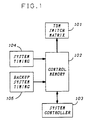
- FIG. 1 shows in simplified block diagram form a typical switch arrangement employing an embodiment of the invention.
- switch matrix 101 which, in this example, is a time division multiplexed (TDM) switch for controllably switching digital signals on incoming communication links to outgoing communication links.
- Control memory 102 supplies control words in so-called control time slots for controlling TDM switch matrix 101 to select the desired switch connections for the digital TDM signals on the incoming links to the outgoing links.
- System controller 103 supplies the control words which are stored in control memory 102, in well-known fashion.
- System timing unit 104 provides primary system timing reference signals which are generated, in well-known fashion.
- Backup system timing unit 105 provides an alternate source of the primary system timing reference signals.
- the timing reference signal commonly referred to as the CLOCK signal, is at a rate of approximately 27 mega Hz.
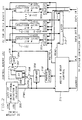
- FIG. 2 depicts in simplified block diagram form details of control memory 102 including a preferred embodiment of the invention. Accordingly, shown are a plurality of shift registers 201-1 through 201-M. Each of shift registers 201-1 through 201-M has N stages and is connected in recirculating configuration via circuit path 202-1 through 202-M, respectively.
- shift registers 201 are of the so-called dynamic type. Use of dynamic shift registers provides a memory matrix of minimum area and, hence, minimum cost. Consequently, more area is available for other circuit components in such systems.
- Select units 203-1 through 203-M are associated on a one-to-one basis with shift registers 201-1 through 201-M, respectively, and are used normally to recirculate the data bits. Additionally, select units 203-1 through 203-M are employed to controllably write control words in parallel from system controller 103 (FIG. 1) into the MxN memory matrix formed by shift registers 201-1 through 201-M.
- M and N may each be any desired integer number. In one example, not to be construed as limiting the scope of the invention, M is 10 and N is 16. N also corresponds to a data frame for TDM switch matrix 101 (FIG. 1).
- control memory 102 is expandable by a desired number of MxN memory matrix units. In a specific example, 16 such MxN control memory matrix units are employed.
- a control word to be inserted into a control time slot in the memory matrix in this example, includes 10 bits. Eight of the control word bits include a switch address, while the two remaining bits are used for so-called overhead.
- the control words in the control time slots are sequentially advanced in shift registers 201 and sequentially supplied to TDM switch matrix 101 (FIG. 1) via SCK signals from CLK generator 204.
- CLK generator 204 generates a pair of sc-called non-overlapping SCK signals in response to the system CLOCK signal, in well-known fashion.
- the non-overlapping SCK signal pair is used to clock the dynamic shift registers 202-1 through 202-M.
- the SCK signal pair is also shown as being supplied to marker storage unit 210 which, in this example, is also a N-bit dynamic shift register.
- marker storage unit 210 which, in this example, is also a N-bit dynamic shift register.
- the system CLOCK and SYNC timing signals are obtained from either system timing unit 104 or backup system timing unit 105 (FIG. 1) under control of loss of timing signal detector and selector 205. Operation of loss of timing signal detector and selector 205 is straightforward.
- a switch is made to the backup system timing unit 105 (FIG. 1).
- the relationship between the system CLOCK signal and system SYNC signal is shown in FIG. 3. As shown in this example, a SYNC pulse is generated at the beginning of each TDM data frame which, in this example, is 16 CLOCK pulses.
- CLOCK is supplied to a clock input of flip-flop 206 and one input of AND gate 207.
- flip-flop 206 An output from flip-flop 206 is supplied to a second input of AND gate 207.
- Flip-flop 206 in this example, is a D type which operates to output the state of the signal supplied to its D input upon the occurrence of the next CLOCK pulse being supplied to its clock input.
- Flip-flop 206 and AND gate 207 form an inhibitor for controllably inhibiting CLK generator 204 to thereby inhibit generation of a SCK pulse pair. Such inhibition of SCK, in turn, inhibits advancing of the control words in shift registers 201 and the timing marker in marker storage unit 210 .
- System SYNC is supplied to one input of NAND gate 208, compare circuit 209 and write and read control 211.
- Write and read control 211 responds to address, SYNC and write/read (W/R) control signals from system controller 103 (FIG. 1) to write a timing marker signal into marker storage unit 210 at an appropriate address.
- the timing marker storage address corresponds to time slot zero (0).
- write and read control 211 responds to address signals, SYNC and the appropriate write control signal to write the control words into shift register 201 via select units 203 as desired.
- System SYNC provides a reference for writing the control words into appropriate control time slots in the control memory matrix.
- Write and read control 211 is also responsive to address signals and a read control signal from system controller 103 to generate a read signal to enable latch 212 to temporarily store the control words recirculating in shift registers 201.
- the control words stored in latch 212 are supplied to system controller 103 for verification purposes.
- An output from marker storage unit 210 is supplied to compare unit 209.
- Compare unit 209 compares whether or not the timing marker stored and being advanced in marker storage unit 210 is in synchronism with the system SYNC signal.
- An output from compare unit 209 is supplied. to a second input of NAND gate 208. Normally, the output from compare unit 209 is a low state corresponding to a logical 0. When there is no match between system SYNC and the output from marker storage unit 210, the output from compare unit 209 is a high state corresponding to a logical 1, as shown in FIG. 4. Normally, the output of NAND gate 208 is a high state corresponding to a logical 1, also shown in FIG. 4.
- compare unit 209 and NAND gate 208 form a comparator for generating a control signal which is a logical 0 whenever the timing marker does not occur concurrently with SYNC.
- This logical 0 output is applied to the D input of flip-flop 206 and upon the occurrence of the next CLOCK pulse supplied to the clock input of flip-flop 206, a low state corresponding to a logical 0 is generated at the output of flip-flop 206.
- This low state output from flip-flop 206 inhibits AND gate 207 from supplying a CLOCK pulse to CLK generator 204. Consequently, generation of a SCK pulse pair is inhibited (FIG. 4) which, in turn, inhibits advancing of the control words in the memory time slots of shift registers 201 and the timing marker in marker storage unit 210. Consequently, the control word advance in shift registers 201 and the timing marker advance in marker storage unit 210 are delayed one time slot interval during the TDM data frame and, in this example, will then be in synchronism for the next TDM data frame, as shown in FIG. 4. If the timing marker was out of synchronism by more than one time slot, additional inhibition cycles would be required up to a total of, in this example, fifteen (15). It is noted that only one SCK pulse pair is inhibited during TDM data frame. Consequently, in this example, for the worse case a total of 15 TDM data frames will be traversed prior to re-establishing synchronization with system timing.
Landscapes
- Engineering & Computer Science (AREA)
- Computer Networks & Wireless Communication (AREA)
- Time-Division Multiplex Systems (AREA)
- Synchronisation In Digital Transmission Systems (AREA)
- Shift Register Type Memory (AREA)
- Use Of Switch Circuits For Exchanges And Methods Of Control Of Multiplex Exchanges (AREA)
- Data Exchanges In Wide-Area Networks (AREA)
Claims (7)
- Dispositif de mémoire de commande (102) comportant une pluralité de registres à décalage (201-1 à 201-M) connectés chacun en une configuration à circulation et disposés pour former une matrice de cellules de stockage pour stocker des binaires de données; une source (205) de signal de cadencement de système (HORLOGE) et de signal de synchronisation de système (SYNC), les binaires de données étant disposés dans des trames de données délimitées par des signaux de synchronisation de système successifs (SYNC) ; et un dispositif (210) pour stocker un marqueur de cadencement; le dispositif de mémoire de commande étant CARACTERISE PAR un dispositif (201-1 à 201-M, 204, 207, 210) sensible audit signal de cadencement de système (HORLOGE) pour avancer les binaires dans ladite pluralité de registres à décalage (201-1 à 201-M) et pour avancer ledit marqueur de cadencement dans ledit dispositif (210) pour le stocker simultanément aux binaires dans la pluralité de registres à décalage; un dispositif (209) pour détecter quand ledit marqueur de cadencement est désynchronisé par rapport audit signal de synchronisation de système (SYNC); et un dispositif (204, 206, 207, 208, 209) pour inhiber l'avancée desdits binaires dans ladite pluralité de registres à décalage (201-1 à 201-M) et pour inhiber simultanément l'avancée dudit marqueur de cadencement dans ledit dispositif (210) de stockage pendant un intervalle prédéterminé durant chaque trame de données pendant laquelle ledit marqueur de cadencement est détecté comme étant désynchronisé par rapport audit signal de synchronisation (SYNC).
- Dispositif selon la revendication 1, dans lequel ladite trame de données comporte un nombre prédéterminé d'intervalles de tranches de temps et ledit intervalle prédéterminé de ladite trame de données est un intervalle de tranche de temps.
- Dispositif selon la revendication 1, dans lequel ledit dispositif de détection comporte un moyen comparateur (208 et 209) sensible à une sortie dudit dispositif (210) pour stocker ledit marqueur de cadencement et audit signal de synchronisation de système (SYNC) pour générer un signal de commande représentatif du fait qu'il n'existe pas de correspondance entre un signal à la sortie dudit dispositif (210) de stockage dudit marqueur de cadencement et ledit signal de synchronisation de système (SYNC).
- Dispositif selon la revendication 3, dans lequel ledit dispositif d'avancée comporte un dispositif (204) pour fournir un signal d'horloge représentatif dudit signal de cadencement de système à ladite pluralité de registres à décalage (201-1 à 201-M) et audit dispositif (210) de stockage dudit marqueur de cadencement, et ledit dispositif d'inhibition comporte un dispositif (206,207) sensible audit signal de commande et audit signal de cadencement de système pour inhiber la fourniture dudit signal d'horloge pendant ledit intervalle prédéterminé.
- Dispositif selon la revendication 4, dans lequel ledit dispositif (210) de stockage dudit marqueur de cadencement comporte un registre à décalage connecté en une configuration à circulation.
- Dispositif selon la revendication 5, dans lequel chacun desdits registres à décalage à N étages.
- Dispositif selon la revendication 6, dans lequel chacun desdits registres à décalage est un registre à décalage dynamique, et ledit dispositif de fourniture dudit signal de cadencement de système est adapté pour fournir un signal d'horloge non chevauchant.
Applications Claiming Priority (2)
| Application Number | Priority Date | Filing Date | Title |
|---|---|---|---|
| US185653 | 1988-04-25 | ||
| US07/185,653 US4873663A (en) | 1988-04-25 | 1988-04-25 | Control memory using recirculating shift registers for a TDM switching apparatus |
Publications (3)
| Publication Number | Publication Date |
|---|---|
| EP0339838A2 EP0339838A2 (fr) | 1989-11-02 |
| EP0339838A3 EP0339838A3 (fr) | 1992-05-27 |
| EP0339838B1 true EP0339838B1 (fr) | 1996-07-03 |
Family
ID=22681899
Family Applications (1)
| Application Number | Title | Priority Date | Filing Date |
|---|---|---|---|
| EP89303678A Expired - Lifetime EP0339838B1 (fr) | 1988-04-25 | 1989-04-13 | Mémoire de commande à registrer à décalage |
Country Status (6)
| Country | Link |
|---|---|
| US (1) | US4873663A (fr) |
| EP (1) | EP0339838B1 (fr) |
| JP (1) | JPH0761171B2 (fr) |
| KR (1) | KR950008650B1 (fr) |
| CA (1) | CA1321023C (fr) |
| DE (1) | DE68926759T2 (fr) |
Families Citing this family (9)
| Publication number | Priority date | Publication date | Assignee | Title |
|---|---|---|---|---|
| EP0363031B1 (fr) * | 1988-09-20 | 1994-11-17 | Fujitsu Limited | Mémoire à semi-conducteur avec entrée/sortie en série |
| USRE38379E1 (en) * | 1989-08-28 | 2004-01-06 | Hitachi, Ltd. | Semiconductor memory with alternately multiplexed row and column addressing |
| KR940008295B1 (ko) * | 1989-08-28 | 1994-09-10 | 가부시기가이샤 히다찌세이사꾸쇼 | 반도체메모리 |
| SE501884C2 (sv) * | 1993-10-12 | 1995-06-12 | Ellemtel Utvecklings Ab | Synkroniserande kretsarrangemang fastställer gräns mellan konsekutiva paket |
| US5666358A (en) * | 1995-10-16 | 1997-09-09 | General Instrument Corporation Of Delaware | Method and apparatus for supporting TDMA operating over hybrid fiber coaxial (HFC) or other channels |
| USRE38619E1 (en) * | 1995-10-16 | 2004-10-12 | General Instrument Corporation | Method and apparatus for supporting TDMA operating over hybrid fiber coaxial (HFC) or other channels |
| US5844942A (en) * | 1997-02-27 | 1998-12-01 | Northrop Grumman Corporation | Pulse position modulation communications protocol |
| US6980563B2 (en) * | 2000-04-13 | 2005-12-27 | International Business Machines Corporation | Method and system for fast ethernet serial port multiplexing to reduce I/O pin count |
| FR2888328B1 (fr) * | 2005-07-08 | 2013-09-20 | Horiba Abx Sas | Procede automatise de preparation d'analyse d'echantillons de sang total et dispositif automatise pour sa mise en oeuvre |
Family Cites Families (11)
| Publication number | Priority date | Publication date | Assignee | Title |
|---|---|---|---|---|
| US2527650A (en) * | 1947-12-24 | 1950-10-31 | Bell Telephone Labor Inc | Synchronization of pulse transmission systems |
| US3639693A (en) * | 1968-11-22 | 1972-02-01 | Stromberg Carlson Corp | Time division multiplex data switch |
| US3742466A (en) * | 1971-11-24 | 1973-06-26 | Honeywell Inf Systems | Memory system for receiving and transmitting information over a plurality of communication lines |
| FR2212055A5 (fr) * | 1972-12-21 | 1974-07-19 | Constr Telephoniques | |
| US4061880A (en) * | 1975-03-21 | 1977-12-06 | Dicom Systems, Ltd. | Time-multiplex programmable switching apparatus |
| US4064370A (en) * | 1976-07-01 | 1977-12-20 | Bell Telephone Laboratories, Incorporated | Time-division switching system |
| US4503490A (en) * | 1981-06-10 | 1985-03-05 | At&T Bell Laboratories | Distributed timing system |
| US4494232A (en) * | 1981-12-04 | 1985-01-15 | Racal-Milgo, Inc. | Statistical multiplexer with dynamic bandwidth allocation for asynchronous and synchronous channels |
| US4740962A (en) * | 1985-12-23 | 1988-04-26 | Motorola, Inc. | Synchronizer for time division multiplexed data |
| CA1254629A (fr) * | 1986-03-21 | 1989-05-23 | Peter Faulkner | Systeme de surete pour materiel |
| NZ220548A (en) * | 1986-06-18 | 1990-05-28 | Fujitsu Ltd | Tdm frame synchronising circuit |
-
1988
- 1988-04-25 US US07/185,653 patent/US4873663A/en not_active Expired - Fee Related
-
1989
- 1989-04-04 CA CA000595591A patent/CA1321023C/fr not_active Expired - Fee Related
- 1989-04-13 EP EP89303678A patent/EP0339838B1/fr not_active Expired - Lifetime
- 1989-04-13 DE DE68926759T patent/DE68926759T2/de not_active Expired - Fee Related
- 1989-04-21 JP JP1100370A patent/JPH0761171B2/ja not_active Expired - Fee Related
- 1989-04-24 KR KR1019890005355A patent/KR950008650B1/ko not_active Expired - Fee Related
Also Published As
| Publication number | Publication date |
|---|---|
| CA1321023C (fr) | 1993-08-03 |
| DE68926759D1 (de) | 1996-08-08 |
| EP0339838A2 (fr) | 1989-11-02 |
| KR950008650B1 (ko) | 1995-08-03 |
| US4873663A (en) | 1989-10-10 |
| JPH0761171B2 (ja) | 1995-06-28 |
| DE68926759T2 (de) | 1996-11-07 |
| JPH0278100A (ja) | 1990-03-19 |
| KR890016870A (ko) | 1989-11-30 |
| EP0339838A3 (fr) | 1992-05-27 |
Similar Documents
| Publication | Publication Date | Title |
|---|---|---|
| EP0026602B1 (fr) | Procédé d'écrire dans et de lire d'une mémoire d'un système de mémoire tampon et système de mémoire tampon utilisant un tel procédé | |
| US4873663A (en) | Control memory using recirculating shift registers for a TDM switching apparatus | |
| US4698806A (en) | Frame alignment of tributaries of a t.d.m. bit stream | |
| US5677931A (en) | Transmission path switching apparatus | |
| US4894821A (en) | Time division switching system with time slot alignment circuitry | |
| US4307462A (en) | Synchronous demultiplexer with elastic dual-memory bit store for TDM/PCM telecommunication system | |
| US4689784A (en) | Data distributor capable of selecting an optional partial data signal and distribution device comprising a plurality of the data distributors | |
| US4053708A (en) | Asynchronous sample pulse generator | |
| JPH08205211A (ja) | 時分割多重時間スイッチ回路 | |
| US6356505B2 (en) | Internal regeneration of the address latch enable (ALE) signal of a protocol of management of a burst interleaved memory and related circuit | |
| GB2066627A (en) | P.C.M. frame aligner with frame slip characteristic | |
| JP2770584B2 (ja) | フレーム位相同期回路 | |
| JPS5939192A (ja) | 時分割スイツチの同期回路 | |
| JP2680141B2 (ja) | フレーム同期方法及びその回路 | |
| JP2702318B2 (ja) | セル位相乗換回路 | |
| JP2799665B2 (ja) | フレーム位相同期装置 | |
| JPS6012890A (ja) | 時分割スイッチ | |
| JP2960761B2 (ja) | Tdma信号用エラスティックバッファ | |
| JPH0681150B2 (ja) | ループネットワーク装置 | |
| JPH03109834A (ja) | フレームアライナ回路 | |
| JPH10257035A (ja) | 伝送装置 | |
| JPH09284262A (ja) | 複数回線の相互同期方法及び相互同期装置 | |
| US20010036244A1 (en) | Accelerated carry generation | |
| JPH06188864A (ja) | 伝送路切替方式 | |
| JPH0453328A (ja) | マルチフレームアライメント回路 |
Legal Events
| Date | Code | Title | Description |
|---|---|---|---|
| PUAI | Public reference made under article 153(3) epc to a published international application that has entered the european phase |
Free format text: ORIGINAL CODE: 0009012 |
|
| AK | Designated contracting states |
Kind code of ref document: A2 Designated state(s): DE FR GB IT SE |
|
| PUAL | Search report despatched |
Free format text: ORIGINAL CODE: 0009013 |
|
| AK | Designated contracting states |
Kind code of ref document: A3 Designated state(s): DE FR GB IT SE |
|
| 17P | Request for examination filed |
Effective date: 19921113 |
|
| RAP3 | Party data changed (applicant data changed or rights of an application transferred) |
Owner name: AT&T CORP. |
|
| 17Q | First examination report despatched |
Effective date: 19940721 |
|
| GRAH | Despatch of communication of intention to grant a patent |
Free format text: ORIGINAL CODE: EPIDOS IGRA |
|
| GRAA | (expected) grant |
Free format text: ORIGINAL CODE: 0009210 |
|
| AK | Designated contracting states |
Kind code of ref document: B1 Designated state(s): DE FR GB IT SE |
|
| ITF | It: translation for a ep patent filed | ||
| ET | Fr: translation filed | ||
| REF | Corresponds to: |
Ref document number: 68926759 Country of ref document: DE Date of ref document: 19960808 |
|
| PLBE | No opposition filed within time limit |
Free format text: ORIGINAL CODE: 0009261 |
|
| STAA | Information on the status of an ep patent application or granted ep patent |
Free format text: STATUS: NO OPPOSITION FILED WITHIN TIME LIMIT |
|
| 26N | No opposition filed | ||
| PGFP | Annual fee paid to national office [announced via postgrant information from national office to epo] |
Ref country code: FR Payment date: 20000322 Year of fee payment: 12 |
|
| PGFP | Annual fee paid to national office [announced via postgrant information from national office to epo] |
Ref country code: SE Payment date: 20000327 Year of fee payment: 12 Ref country code: GB Payment date: 20000327 Year of fee payment: 12 |
|
| PGFP | Annual fee paid to national office [announced via postgrant information from national office to epo] |
Ref country code: DE Payment date: 20000630 Year of fee payment: 12 |
|
| PG25 | Lapsed in a contracting state [announced via postgrant information from national office to epo] |
Ref country code: GB Free format text: LAPSE BECAUSE OF NON-PAYMENT OF DUE FEES Effective date: 20010413 |
|
| PG25 | Lapsed in a contracting state [announced via postgrant information from national office to epo] |
Ref country code: SE Free format text: LAPSE BECAUSE OF NON-PAYMENT OF DUE FEES Effective date: 20010414 |
|
| PG25 | Lapsed in a contracting state [announced via postgrant information from national office to epo] |
Ref country code: FR Free format text: THE PATENT HAS BEEN ANNULLED BY A DECISION OF A NATIONAL AUTHORITY Effective date: 20010430 |
|
| EUG | Se: european patent has lapsed |
Ref document number: 89303678.0 |
|
| GBPC | Gb: european patent ceased through non-payment of renewal fee |
Effective date: 20010413 |
|
| REG | Reference to a national code |
Ref country code: FR Ref legal event code: ST |
|
| PG25 | Lapsed in a contracting state [announced via postgrant information from national office to epo] |
Ref country code: DE Free format text: LAPSE BECAUSE OF NON-PAYMENT OF DUE FEES Effective date: 20020301 |
|
| PG25 | Lapsed in a contracting state [announced via postgrant information from national office to epo] |
Ref country code: IT Free format text: LAPSE BECAUSE OF NON-PAYMENT OF DUE FEES;WARNING: LAPSES OF ITALIAN PATENTS WITH EFFECTIVE DATE BEFORE 2007 MAY HAVE OCCURRED AT ANY TIME BEFORE 2007. THE CORRECT EFFECTIVE DATE MAY BE DIFFERENT FROM THE ONE RECORDED. Effective date: 20050413 |