EP0344715A2 - Integrierte Halbleiterschaltung mit Temperaturerfassungsanordnung - Google Patents
Integrierte Halbleiterschaltung mit Temperaturerfassungsanordnung Download PDFInfo
- Publication number
- EP0344715A2 EP0344715A2 EP89109740A EP89109740A EP0344715A2 EP 0344715 A2 EP0344715 A2 EP 0344715A2 EP 89109740 A EP89109740 A EP 89109740A EP 89109740 A EP89109740 A EP 89109740A EP 0344715 A2 EP0344715 A2 EP 0344715A2
- Authority
- EP
- European Patent Office
- Prior art keywords
- circuit
- voltage
- transistor
- bias
- temperature
- Prior art date
- Legal status (The legal status is an assumption and is not a legal conclusion. Google has not performed a legal analysis and makes no representation as to the accuracy of the status listed.)
- Withdrawn
Links
Images

Classifications
-
- G—PHYSICS
- G11—INFORMATION STORAGE
- G11C—STATIC STORES
- G11C7/00—Arrangements for writing information into, or reading information out from, a digital store
- G11C7/04—Arrangements for writing information into, or reading information out from, a digital store with means for avoiding disturbances due to temperature effects
-
- H—ELECTRICITY
- H02—GENERATION; CONVERSION OR DISTRIBUTION OF ELECTRIC POWER
- H02H—EMERGENCY PROTECTIVE CIRCUIT ARRANGEMENTS
- H02H7/00—Emergency protective circuit arrangements specially adapted for specific types of electric machines or apparatus or for sectionalised protection of cable or line systems, and effecting automatic switching in the event of an undesired change from normal working conditions
- H02H7/20—Emergency protective circuit arrangements specially adapted for specific types of electric machines or apparatus or for sectionalised protection of cable or line systems, and effecting automatic switching in the event of an undesired change from normal working conditions for electronic equipment
-
- G—PHYSICS
- G01—MEASURING; TESTING
- G01R—MEASURING ELECTRIC VARIABLES; MEASURING MAGNETIC VARIABLES
- G01R31/00—Arrangements for testing electric properties; Arrangements for locating electric faults; Arrangements for electrical testing characterised by what is being tested not provided for elsewhere
- G01R31/26—Testing of individual semiconductor devices
-
- G—PHYSICS
- G11—INFORMATION STORAGE
- G11C—STATIC STORES
- G11C5/00—Details of stores covered by group G11C11/00
- G11C5/14—Power supply arrangements, e.g. power down, chip selection or deselection, layout of wirings or power grids, or multiple supply levels
- G11C5/147—Voltage reference generators, voltage or current regulators; Internally lowered supply levels; Compensation for voltage drops
-
- H—ELECTRICITY
- H02—GENERATION; CONVERSION OR DISTRIBUTION OF ELECTRIC POWER
- H02H—EMERGENCY PROTECTIVE CIRCUIT ARRANGEMENTS
- H02H5/00—Emergency protective circuit arrangements for automatic disconnection directly responsive to an undesired change from normal non-electric working conditions with or without subsequent reconnection
- H02H5/04—Emergency protective circuit arrangements for automatic disconnection directly responsive to an undesired change from normal non-electric working conditions with or without subsequent reconnection responsive to abnormal temperature
- H02H5/044—Emergency protective circuit arrangements for automatic disconnection directly responsive to an undesired change from normal non-electric working conditions with or without subsequent reconnection responsive to abnormal temperature using a semiconductor device to sense the temperature
Definitions
- the present invention generally relates to semiconductor integrated circuit devices, and more particularly to a semiconductor integrated circuit device having a function of protecting a large scale integrated circuit from a thermal destruction caused by a rise in temperature.
- a cooling system for cooling the LSI is changing from an air cooled system to a forced air cooled system and a liquid cooled system.
- the temperature of the LSI which is operating rises quickly and in some cases instantaneously reaches a destruction temperature. Accordingly, it is necessary to detect the rise in the LSI temperature before it reaches the destruction temperature and stop the heat generation of the LSI so as to protect the LSI from thermal destruction by the self-generated heat.
- a protection circuit for protecting the LSI from thermal destruction is provided not within the LSI but externally to the LSI in a device on which the LSI is mounted.
- the protection circuit monitors the air temperature within the device or the operation of a motor which drives a cooling fan.
- the protection circuit cuts off the supply of power to the LSI so as to stop the heat generation of the LSI and accordingly prevent the thermal destruction.
- a Japanese Laid-Open Patent Application No.56-120153 proposes an integrated circuit having a temperature protector provided inside the integrated circuit.
- a power source voltage required to drive the temperature protector is greater than a power source voltage required by the integrated circuit.
- the power consumption of this proposed integrated circuit is large.
- Another and more specific object of the present invention is to provide a semiconductor integrated circuit device formed on a single substrate and comprising a first power source, a second power source for supplying a voltage different from a voltage supplied by the first power source, an emitter coupled logic circuit including a pair of first transistors having emitters thereof connected in common and collectors thereof operatively coupled to the first power source and a second transistor having a collector thereof connected to the emitters of the first transistors and an emitter thereof operatively coupled to the second power source, where the second transistor supplies a current to the first transistors, a bias circuit for supplying a bias voltage to a base of the second transistor, where the bias voltage has a first voltage in a normal operating state, a temperature sensor provided in a vicinity of the emitter coupled logic circuit for detecting a temperature, and an abnormal temperature detection circuit coupled between the temperature sensor and the bias circuit for outputting an abnormal temperature signal when the temperature detected by the temperature sensor exceeds a predetermined value.
- the bias circuit includes means for changing the bias voltage from the first voltage to a second voltage which is different from the first voltage responsive to the abnormal temperature signal from the abnormal temperature detection circuit in a shut-down state so that the second transistor of the emitter coupled logic circuit is turned OFF. According to the semiconductor integrated circuit device of the present invention, it is possible to quickly detect a rise in the temperature of the emitter coupled logic circuit (that is, the LSI) and positively prevent thermal destruction thereof.
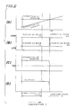
- FIG.1 shows an embodiment of a semiconductor integrated circuit device according to the present invention.
- the semiconductor integrated circuit device has a large scale integrated circuit (LSI) 10 which is to be protected from thermal destruction, a temperature sensor 20 for protecting the LSI 10 from abnormal temperatures, an abnormal temperature detection circuit 30, and a bias circuit 40 having a shut-down function.
- the LSI 10, the temperature sensor 20, the abnormal temperature detection circuit 30, and the bias circuit 40 are provided on a common single substrate (not shown) of the semiconductor integrated circuit device.
- the LSI 10 is made up of an emitter coupled logic (ECL) circuit including a transistor Q15 for supplying a constant current I cs to a current switch circuit and a transistor Q16 for supplying a constant current I ef to an emitter follower circuit.
- the transistor Q15 of the current switch circuit is coupled to a collector voltage source V cc through a transistor Q11 which receives a first input I1 from a terminal 61, a transistor Q12 which receives a second input I2 from a terminal 62, and a transistor Q13 which receives a reference voltage V bb from a circuit which will be described later in conjunction with FIG.3.
- the current switch circuit is connected to an emitter voltage source V ee .
- the transistor Q16 of the emitter follower circuit is coupled to the collector voltage source V cc through a transistor Q14.
- a base of the transistor Q14 is connected to a collector of the transistor Q13.
- An OR output signal from an emitter of the transistor Q14 is output from an output terminal 63.
- a bias voltage V cs which will be described later is applied to bases of the transistors Q15 and Q16.
- the temperature sensor 20 detects the temperature of the LSI 10 by use of the fact that a diode D and a resistor R have mutually different temperature coefficients and supplies voltages which are dependent on the detected temperature to the abnormal temperature detection circuit 30.
- the temperature sensor 20 is provided in a vicinity of the LSI 10, and is provided at a central portion of the substrate in this embodiment.
- the diode D and the resistor R are connected in series to respective constant current sources S1 and S2.
- the output voltages of the temperature sensor 20 are obtained from a node N1 which connects the diode D and the constant current source S1 and from a node N2 which connects the resistor R and the constant current source S2.
- the nodes N1 and N2 correspond to output terminals of the temperature sensor 20.
- the abnormal temperature detection circuit 30 includes a comparator CP and a latch circuit L.
- the output voltages of the temperature sensor 20 are supplied to the comparator CP.
- the temperature sensor 20 is designed so that the potential at the node N1 is lower than the potential at the node N2 at the normal operating temperatures.
- a temperature T of the LSI 10 rises, the terminal voltage of the diode D decreases while the resistance of the resistor R virtually remains unchanged.
- the polarity of the voltage across the nodes N1 and N2 becomes inverted about a predetermined temperature T0 where the potentials at the nodes N1 and N2 become equal, as shown in FIG.2(A). That is, the polarities of the input voltages of the comparator CP are inverted about the predetermined temperature T0, and a logic output of the comparator CP is inverted accordingly.
- the latch circuit L stores an output inversion of the comparator CP and outputs the output inversion as an abnormal temperature signal.
- the output inversion of the latch circuit L continues until a reset signal is applied to a reset terminal R s .
- a node N3 is at a high level and a node N4 is at a low level, and the output inversion occurs due to the temperature rise of the LSI 10 as shown in FIG.2(B).
- the nodes N3 and N4 correspond to output terminals of the abnormal temperature detection circuit 30.
- the predetermined temperature T0 is set to a value which is higher than a maximum temperature (for example, in the order of 125 °C) at which the operation of the LSI 10 is guaranteed. For example, it is appropriate to set the predetermined temperature T0 within a temperature range of 150 °C to 200 °C in which the functional operation of the LSI 10 is correct.
- the predetermined temperature T0 is set in this manner by appropriately selecting the values and characteristics of the diode D, the resistor R and the constant current sources S1 and S2.
- the bias circuit 40 having the shut-down function is made up of a shut-down part 41 which includes transistors Q1 through Q5, and a bias circuit part 42 which includes transistors Q6 through Q10.
- An output signal of the shut-down part 41 is obtained from a node N5, and an output signal of the bias circuit part 42 is obtained from a node N6.
- the transistors Q1 and Q2 form an input portion of the shut-down part 41, and the transistors Q3 and Q4 form a current mirror circuit.
- a collector of the transistor Q3 is coupled to an emitter of the transistor Q1 through a resistor R1, while a collector of the transistor Q4 is coupled to an emitter of the transistor Q2 through a resistor R2.
- the resistors R1 and R2 have identical resistances.
- the collector of the transistor Q4 is also connected to a base of the transistor Q5, and the collector of the transistor Q5 is also connected to the node N5 which corresponds to an output terminal of the shut-down part 42.
- the node N3 is at the high level and the node N4 is at the low level during the normal operation.
- identical currents constantly flow through the transistors Q3 and Q4.
- the resistances of the resistors R1 and R2 are the same. Accordingly, the voltage difference between the nodes N3 and N4 appear between the collectors of the transistors Q3 and Q4, and the collector voltage of the transistor Q4 becomes a predetermined value ⁇ V (voltage difference between the nodes N3 and N4) lower than the collector voltage of the transistor Q3. As a result, the transistor Q5 is cut off.
- the bias circuit part 42 has the transistors Q6 through Q10 and resistors R3 through R7.
- the bias circuit part 42 When the transistor Q5 of the shut-down part 41 is cut off, the bias circuit part 42 generates a bias voltage V cs at the node N6 by a normal operation and supplies this bias voltage V sc to the LSI 10.
- a control is carried out so that the current I cs is supplied to the transistor Q15 which constitutes the current switch circuit within the LSI 10 and the current I ef is supplied to the transistor Q16 which constitutes the emitter follower circuit within the LSI 10.
- the shut-down function of the shut-down part 41 is activated by the abnormal temperature signal from the abnormal temperature detection circuit 30, and no current flows to the LSI 10.
- the potential at the node N1 becomes higher than that at the node N2 in this case, and consequently, the levels at the nodes N3 and N4 respectively become high and low thereby turning the transistor Q5 ON.
- a collector current of this transistor Q5 flows through the resistor R3 and the voltage at the node N5 drops to approximately a saturation voltage (for example, in the order of 0.1 V) between the collector and emitter of the transistor Q5.
- the transistor Q8 is cut off, and the voltage V cs at the node N6 drops to the minimum voltage V ee as shown in FIG.2(C).
- the transistors Q15 and Q16 which are used as constant current sources in the LSI 10 are cut off, and the currents I cs and I ef no longer flow as shown in FIG.2(D). Therefore, the heat generation of the LSI 10 stops and the temperature T of the LSI 10 (that is, the chip temperature) decreases.
- the reset terminal R s of the abnormal temperature detection circuit 30 is normally at a low level.
- the latch circuit L stores the output inversion of the comparator CP and the output inversion of the latch circuit L continues until the reset signal is applied to the reset terminal R s .
- the latch circuit L is provided to prevent an unstable operation of the shut-down part 41 which may occur when the temperature T detected by the temperature sensor 20 fluctuates within a certain temperature range. However, it is possible to return the bias circuit 40 to the normal operating state from the shut-down state by applying a high-level reset signal to the reset terminal R s .
- a monitoring terminal 65 may be connected to any of the nodes N3 through N6 for the purpose of monitoring the state of the bias circuit 40, that is, whether the bias circuit 40 is in the normal operating state or the shut-down state.
- the monitoring terminal 65 is shown as being connected to the node N3 for the sake of convenience. In this case, it is possible to detect that the bias circuit 40 is in the normal operating state when the signal level at the monitoring terminal 65 is high and is in the shut-down state when the signal level at the monitoring terminal 65 is low.
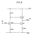
- FIG.3 shows the circuit which generates the reference voltage V bb which is supplied to a base of the transistor Q13 of the LSI 10.
- a reference voltage generating circuit 50 is coupled to a terminal 64 which connects to the node N6.
- the reference voltage generating circuit 50 includes a resistor R51, a transistor Q51, and a resistor R52 which are connected in series between the voltage sources V cc and V ee , and transistors Q52 and Q53 and a resistor R53 which are connected in series between the voltage sources V cc and V ee .
- the voltage V cs from the terminal 64 is supplied to bases of the transistors Q51 and Q53.
- a base of the transistor Q52 is connected to a collector of the transistor Q51.
- a terminal 67 is connected to a node which connects a collector of the transistor Q53 and an emitter of the transistor Q52, and the reference voltage V bb is output from this terminal 67.
- the LSI 10 is made up of one current switch circuit and one emitter follower circuit for the sake of convenience.
- the LSI 10 has a plurality of current switch circuits and emitter follower circuits, and the heat generation mainly occurs at these parts of the LSI 10.
- a current slightly flows through the temperature sensor 20, the abnormal temperature detection circuit 30, and the bias circuit 40 even in the shut-down state, but the number of elements constituting these circuits is small and the heat generated thereby is virtually negligible.
- the shut-down function is activated when the temperature T of the LSI 10 exceeds the predetermined temperature T0, and the heat generation of the LSI 10 is greatly reduced. Therefore, it is possible to positively protect the LSI 10 from thermal destruction. It is expected that the integration density and the power consumption of the bipolar LSI will further increase in the future, and the present invention is applicable to such a bipolar LSI for the purpose of positively preventing the thermal destruction.
- the LSI 10 is shown as a simple ECL circuit.
- the present invention is similarly applicable to other types of LSIs having a bias circuit for the constant current source.
- the temperature sensor 20 of the embodiment is made up of the diode D and the resistor R. However, it is of course possible to constitute the temperature sensor 20 from other elements as long as the elements can be formed on the substrate of the semiconductor integrated circuit device and can detect the temperature rise.
Landscapes
- Engineering & Computer Science (AREA)
- Power Engineering (AREA)
- Physics & Mathematics (AREA)
- General Physics & Mathematics (AREA)
- Semiconductor Integrated Circuits (AREA)
- Measuring Temperature Or Quantity Of Heat (AREA)
- Bipolar Integrated Circuits (AREA)
Applications Claiming Priority (2)
| Application Number | Priority Date | Filing Date | Title |
|---|---|---|---|
| JP133659/88 | 1988-05-31 | ||
| JP63133659A JPH01302849A (ja) | 1988-05-31 | 1988-05-31 | 半導体集積回路装置 |
Publications (2)
| Publication Number | Publication Date |
|---|---|
| EP0344715A2 true EP0344715A2 (de) | 1989-12-06 |
| EP0344715A3 EP0344715A3 (de) | 1991-03-27 |
Family
ID=15109938
Family Applications (1)
| Application Number | Title | Priority Date | Filing Date |
|---|---|---|---|
| EP19890109740 Withdrawn EP0344715A3 (de) | 1988-05-31 | 1989-05-30 | Integrierte Halbleiterschaltung mit Temperaturerfassungsanordnung |
Country Status (3)
| Country | Link |
|---|---|
| EP (1) | EP0344715A3 (de) |
| JP (1) | JPH01302849A (de) |
| KR (1) | KR900019221A (de) |
Cited By (1)
| Publication number | Priority date | Publication date | Assignee | Title |
|---|---|---|---|---|
| CN100389308C (zh) * | 2004-05-26 | 2008-05-21 | 鸿富锦精密工业(深圳)有限公司 | 芯片温测装置及其温测方法 |
Families Citing this family (10)
| Publication number | Priority date | Publication date | Assignee | Title |
|---|---|---|---|---|
| US5461252A (en) * | 1992-10-06 | 1995-10-24 | Matsushita Electric Industrial Co., Ltd. | Semiconductor device comprising an over-temperature detection element for detecting excessive temperature of amplifiers |
| JP3869815B2 (ja) | 2003-03-31 | 2007-01-17 | Necエレクトロニクス株式会社 | 半導体集積回路装置 |
| JP3810411B2 (ja) | 2004-01-23 | 2006-08-16 | Necエレクトロニクス株式会社 | 集積回路装置 |
| JP4541717B2 (ja) | 2004-02-09 | 2010-09-08 | ルネサスエレクトロニクス株式会社 | 集積回路装置及びその製造方法 |
| JP4541742B2 (ja) | 2004-03-30 | 2010-09-08 | ルネサスエレクトロニクス株式会社 | 集積回路装置 |
| JP4536408B2 (ja) | 2004-03-30 | 2010-09-01 | ルネサスエレクトロニクス株式会社 | 集積回路装置 |
| JP4620962B2 (ja) | 2004-03-30 | 2011-01-26 | ルネサスエレクトロニクス株式会社 | 集積回路装置の製造方法及び酸化バナジウム膜の形成方法 |
| JP4535367B2 (ja) | 2004-05-24 | 2010-09-01 | ルネサスエレクトロニクス株式会社 | 集積回路装置 |
| KR100736403B1 (ko) * | 2005-08-19 | 2007-07-09 | 삼성전자주식회사 | 온도 검출기, 온도 검출방법, 및 상기 온도 검출기를구비하는 반도체 장치 |
| JP4524688B2 (ja) * | 2007-01-23 | 2010-08-18 | エルピーダメモリ株式会社 | 基準電圧発生回路及び半導体集積回路装置 |
Family Cites Families (5)
| Publication number | Priority date | Publication date | Assignee | Title |
|---|---|---|---|---|
| US3916263A (en) * | 1971-12-13 | 1975-10-28 | Honeywell Inf Systems | Memory driver circuit with thermal protection |
| DE3415764A1 (de) * | 1984-04-27 | 1985-10-31 | Siemens AG, 1000 Berlin und 8000 München | Schaltungsanordnung zur temperaturueberwachung integrierter schaltungen |
| US4667265A (en) * | 1985-12-20 | 1987-05-19 | National Semiconductor Corporation | Adaptive thermal shutdown circuit |
| JPS6315528A (ja) * | 1986-07-08 | 1988-01-22 | Nec Corp | 半導体装置 |
| JPS63124618A (ja) * | 1986-11-14 | 1988-05-28 | Nec Corp | 論理ゲ−ト駆動制御回路 |
-
1988
- 1988-05-31 JP JP63133659A patent/JPH01302849A/ja active Pending
-
1989
- 1989-05-30 EP EP19890109740 patent/EP0344715A3/de not_active Withdrawn
- 1989-05-30 KR KR1019890007198A patent/KR900019221A/ko active Granted
Cited By (1)
| Publication number | Priority date | Publication date | Assignee | Title |
|---|---|---|---|---|
| CN100389308C (zh) * | 2004-05-26 | 2008-05-21 | 鸿富锦精密工业(深圳)有限公司 | 芯片温测装置及其温测方法 |
Also Published As
| Publication number | Publication date |
|---|---|
| KR920008421B1 (de) | 1992-09-28 |
| JPH01302849A (ja) | 1989-12-06 |
| EP0344715A3 (de) | 1991-03-27 |
| KR900019221A (ko) | 1990-12-24 |
Similar Documents
| Publication | Publication Date | Title |
|---|---|---|
| US4787007A (en) | Output driver circuit | |
| US5523709A (en) | Power-on reset circuit and method | |
| EP0305098A2 (de) | CMOS/ECL Konverter-Ausgangspufferschaltung | |
| JP2540753B2 (ja) | 過熱検出回路 | |
| EP0344715A2 (de) | Integrierte Halbleiterschaltung mit Temperaturerfassungsanordnung | |
| EP0826272B1 (de) | Schaltkreis zur verbesserung der metastabilen zeitauflösung bei einem flipflop mit niedriger leistungsaufnahme | |
| JP2727809B2 (ja) | 半導体集積回路 | |
| KR100213845B1 (ko) | 집적 전원 공급 모니터회로 | |
| EP0730347A2 (de) | Halbleitervorrichtung | |
| US5543996A (en) | Protective circuit for protecting transistor from thermal destruction | |
| US20080030914A1 (en) | Microelectronic device equipped with a thermal protection circuit and thermal protection method for a microelectronic device | |
| US6201436B1 (en) | Bias current generating circuits and methods for integrated circuits including bias current generators that increase and decrease with temperature | |
| EP0211553A1 (de) | Einschaltrücksetzschaltungsanordnungen | |
| JP2006349521A (ja) | 過熱検出回路および半導体集積回路装置 | |
| JPH0919049A (ja) | 半導体保護回路 | |
| US5285346A (en) | Current driven control circuit for a power device | |
| US7499253B2 (en) | Semiconductor integrated-circuit unit with temperature protective circuit | |
| JP3710616B2 (ja) | トランジスタ保護回路および出力電力増幅回路 | |
| US4565959A (en) | Current supply circuit with redundant back-up current source | |
| JPH01218350A (ja) | 電力用半導体装置 | |
| EP1265363B1 (de) | Einstellbare temperaturkompensierte Schwellwertschaltung mit die Versorgungsspannung überschreitenden Auslösepunkten | |
| JP3226866B2 (ja) | 電源電圧監視回路及び入力信号レベル監視回路 | |
| US5130637A (en) | Constant voltage generating circuit | |
| JP3821899B2 (ja) | BiCMOS/CMOSスイッチング回路 | |
| JP3271545B2 (ja) | 電源電圧立ち上がり時における誤動作防止回路 |
Legal Events
| Date | Code | Title | Description |
|---|---|---|---|
| PUAI | Public reference made under article 153(3) epc to a published international application that has entered the european phase |
Free format text: ORIGINAL CODE: 0009012 |
|
| AK | Designated contracting states |
Kind code of ref document: A2 Designated state(s): DE FR GB |
|
| PUAL | Search report despatched |
Free format text: ORIGINAL CODE: 0009013 |
|
| AK | Designated contracting states |
Kind code of ref document: A3 Designated state(s): DE FR GB |
|
| RHK1 | Main classification (correction) |
Ipc: H02H 5/04 |
|
| STAA | Information on the status of an ep patent application or granted ep patent |
Free format text: STATUS: THE APPLICATION IS DEEMED TO BE WITHDRAWN |
|
| 18D | Application deemed to be withdrawn |
Effective date: 19910930 |