EP0345347B1 - Electrode a transistor a effet de champ (fet) - Google Patents
Electrode a transistor a effet de champ (fet) Download PDFInfo
- Publication number
- EP0345347B1 EP0345347B1 EP87907678A EP87907678A EP0345347B1 EP 0345347 B1 EP0345347 B1 EP 0345347B1 EP 87907678 A EP87907678 A EP 87907678A EP 87907678 A EP87907678 A EP 87907678A EP 0345347 B1 EP0345347 B1 EP 0345347B1
- Authority
- EP
- European Patent Office
- Prior art keywords
- fet
- membrane
- electrode
- ion
- carbon
- Prior art date
- Legal status (The legal status is an assumption and is not a legal conclusion. Google has not performed a legal analysis and makes no representation as to the accuracy of the status listed.)
- Expired - Lifetime
Links
- OKTJSMMVPCPJKN-UHFFFAOYSA-N Carbon Chemical compound [C] OKTJSMMVPCPJKN-UHFFFAOYSA-N 0.000 claims abstract description 31
- 229910052799 carbon Inorganic materials 0.000 claims abstract description 30
- 239000000758 substrate Substances 0.000 claims abstract description 19
- 239000012528 membrane Substances 0.000 claims description 48
- 239000011248 coating agent Substances 0.000 claims description 9
- 238000000576 coating method Methods 0.000 claims description 9
- 239000012212 insulator Substances 0.000 claims description 6
- 102000004190 Enzymes Human genes 0.000 claims description 2
- 108090000790 Enzymes Proteins 0.000 claims description 2
- 230000033116 oxidation-reduction process Effects 0.000 claims description 2
- NXXYKOUNUYWIHA-UHFFFAOYSA-N 2,6-Dimethylphenol Chemical compound CC1=CC=CC(C)=C1O NXXYKOUNUYWIHA-UHFFFAOYSA-N 0.000 abstract description 12
- 150000002500 ions Chemical class 0.000 abstract description 11
- 230000005669 field effect Effects 0.000 abstract description 4
- GPRLSGONYQIRFK-UHFFFAOYSA-N hydron Chemical compound [H+] GPRLSGONYQIRFK-UHFFFAOYSA-N 0.000 abstract 1
- 229920006254 polymer film Polymers 0.000 abstract 1
- 229910052594 sapphire Inorganic materials 0.000 description 12
- 239000010980 sapphire Substances 0.000 description 12
- 230000015572 biosynthetic process Effects 0.000 description 8
- XUIMIQQOPSSXEZ-UHFFFAOYSA-N Silicon Chemical compound [Si] XUIMIQQOPSSXEZ-UHFFFAOYSA-N 0.000 description 7
- 229910052710 silicon Inorganic materials 0.000 description 7
- 239000010703 silicon Substances 0.000 description 7
- 238000004544 sputter deposition Methods 0.000 description 6
- 239000004065 semiconductor Substances 0.000 description 5
- 238000002474 experimental method Methods 0.000 description 4
- WEVYAHXRMPXWCK-UHFFFAOYSA-N Acetonitrile Chemical compound CC#N WEVYAHXRMPXWCK-UHFFFAOYSA-N 0.000 description 3
- VYPSYNLAJGMNEJ-UHFFFAOYSA-N Silicium dioxide Chemical compound O=[Si]=O VYPSYNLAJGMNEJ-UHFFFAOYSA-N 0.000 description 3
- 230000001747 exhibiting effect Effects 0.000 description 3
- 238000005259 measurement Methods 0.000 description 3
- 238000006116 polymerization reaction Methods 0.000 description 3
- 229910052581 Si3N4 Inorganic materials 0.000 description 2
- 239000008186 active pharmaceutical agent Substances 0.000 description 2
- 239000012300 argon atmosphere Substances 0.000 description 2
- 239000012298 atmosphere Substances 0.000 description 2
- 238000009792 diffusion process Methods 0.000 description 2
- 230000000694 effects Effects 0.000 description 2
- 239000007789 gas Substances 0.000 description 2
- 238000009413 insulation Methods 0.000 description 2
- 229910052751 metal Inorganic materials 0.000 description 2
- 239000002184 metal Substances 0.000 description 2
- VNWKTOKETHGBQD-UHFFFAOYSA-N methane Chemical compound C VNWKTOKETHGBQD-UHFFFAOYSA-N 0.000 description 2
- 238000000034 method Methods 0.000 description 2
- 229920000620 organic polymer Polymers 0.000 description 2
- VYZAMTAEIAYCRO-UHFFFAOYSA-N Chromium Chemical compound [Cr] VYZAMTAEIAYCRO-UHFFFAOYSA-N 0.000 description 1
- UFHFLCQGNIYNRP-UHFFFAOYSA-N Hydrogen Chemical compound [H][H] UFHFLCQGNIYNRP-UHFFFAOYSA-N 0.000 description 1
- BQCADISMDOOEFD-UHFFFAOYSA-N Silver Chemical compound [Ag] BQCADISMDOOEFD-UHFFFAOYSA-N 0.000 description 1
- 229910021607 Silver chloride Inorganic materials 0.000 description 1
- 239000000853 adhesive Substances 0.000 description 1
- 230000001070 adhesive effect Effects 0.000 description 1
- QVGXLLKOCUKJST-UHFFFAOYSA-N atomic oxygen Chemical compound [O] QVGXLLKOCUKJST-UHFFFAOYSA-N 0.000 description 1
- 229910052804 chromium Inorganic materials 0.000 description 1
- 239000011651 chromium Substances 0.000 description 1
- 229910052681 coesite Inorganic materials 0.000 description 1
- 239000004020 conductor Substances 0.000 description 1
- 229910052906 cristobalite Inorganic materials 0.000 description 1
- 238000005868 electrolysis reaction Methods 0.000 description 1
- 239000008151 electrolyte solution Substances 0.000 description 1
- 239000010439 graphite Substances 0.000 description 1
- 229910002804 graphite Inorganic materials 0.000 description 1
- 239000012535 impurity Substances 0.000 description 1
- WABPQHHGFIMREM-UHFFFAOYSA-N lead(0) Chemical compound [Pb] WABPQHHGFIMREM-UHFFFAOYSA-N 0.000 description 1
- 239000007788 liquid Substances 0.000 description 1
- 229910044991 metal oxide Inorganic materials 0.000 description 1
- 150000004706 metal oxides Chemical class 0.000 description 1
- 239000000203 mixture Substances 0.000 description 1
- 230000007935 neutral effect Effects 0.000 description 1
- 239000001301 oxygen Substances 0.000 description 1
- 229910052760 oxygen Inorganic materials 0.000 description 1
- 239000008055 phosphate buffer solution Substances 0.000 description 1
- 229920001296 polysiloxane Polymers 0.000 description 1
- 239000000377 silicon dioxide Substances 0.000 description 1
- 235000012239 silicon dioxide Nutrition 0.000 description 1
- HQVNEWCFYHHQES-UHFFFAOYSA-N silicon nitride Chemical compound N12[Si]34N5[Si]62N3[Si]51N64 HQVNEWCFYHHQES-UHFFFAOYSA-N 0.000 description 1
- 229910052814 silicon oxide Inorganic materials 0.000 description 1
- 229920002050 silicone resin Polymers 0.000 description 1
- 229910052709 silver Inorganic materials 0.000 description 1
- 239000004332 silver Substances 0.000 description 1
- HKZLPVFGJNLROG-UHFFFAOYSA-M silver monochloride Chemical compound [Cl-].[Ag+] HKZLPVFGJNLROG-UHFFFAOYSA-M 0.000 description 1
- BAZAXWOYCMUHIX-UHFFFAOYSA-M sodium perchlorate Chemical compound [Na+].[O-]Cl(=O)(=O)=O BAZAXWOYCMUHIX-UHFFFAOYSA-M 0.000 description 1
- 229910001488 sodium perchlorate Inorganic materials 0.000 description 1
- 239000000243 solution Substances 0.000 description 1
- 239000002904 solvent Substances 0.000 description 1
- 229910052682 stishovite Inorganic materials 0.000 description 1
- 229910052905 tridymite Inorganic materials 0.000 description 1
Images

Classifications
-
- G—PHYSICS
- G01—MEASURING; TESTING
- G01N—INVESTIGATING OR ANALYSING MATERIALS BY DETERMINING THEIR CHEMICAL OR PHYSICAL PROPERTIES
- G01N27/00—Investigating or analysing materials by the use of electric, electrochemical, or magnetic means
- G01N27/26—Investigating or analysing materials by the use of electric, electrochemical, or magnetic means by investigating electrochemical variables; by using electrolysis or electrophoresis
- G01N27/28—Electrolytic cell components
- G01N27/30—Electrodes, e.g. test electrodes; Half-cells
-
- G—PHYSICS
- G01—MEASURING; TESTING
- G01N—INVESTIGATING OR ANALYSING MATERIALS BY DETERMINING THEIR CHEMICAL OR PHYSICAL PROPERTIES
- G01N27/00—Investigating or analysing materials by the use of electric, electrochemical, or magnetic means
- G01N27/26—Investigating or analysing materials by the use of electric, electrochemical, or magnetic means by investigating electrochemical variables; by using electrolysis or electrophoresis
- G01N27/403—Cells and electrode assemblies
- G01N27/414—Ion-sensitive or chemical field-effect transistors, i.e. ISFETS or CHEMFETS
Definitions
- This invention relates to a FET electrode and, more particularly, to an ion-sensitive FET electrode.
- FET electrodes utilize the principle of a field-effect transistor (FET).
- FET field-effect transistor
- a p-type substrate which comprises a substrate of a metal oxide/semiconductor insulative membrane (p-type SiO2/Si3N4), on the gate portion thereof, thereby forming an n-type source and a drain electrode.
- p-type SiO2/Si3N4 metal oxide/semiconductor insulative membrane
- the potential of the p-type semiconductor in the vicinity of a redox membrane drops to induce electrons within the p-type semiconductor.
- a layer of these electrons forms a channel along which elections flow from the source to the drain to produce a drain current.
- the amount of this drain current is controlled by the gate voltage. Since the voltage at the gate is proportional to the H+ ion activity, the FET electrode can be used as a pH-MOSFET.
- a FET electrode of this type responds to light, besides exhibiting a large amount of drift and poor stability.
- Another FET electrode described in patent document JP-A-57 63444 uses a metal chromium layer between a gate insulation layer and an organic polymer layer in order to prevent the organic polymer layer from being separated from the gate insulation layer.
- a layer of conductive material such as metal between a gate insulating film and a selective ion sensitive layer is provided in order to produce a small-size semiconductor sensor having uniform characteristics.
- An object of the present invention is to solve the foregoing problems of the prior art and provide a FET electrode exhibiting little drift, high stability and little response to light.
- the FET electrode of the present invention comprises a FET, a carbon thin membrane coating a gate insulator of the FET, and an organic thin membrane coating the carbon thin membrane.
- the FET measures the concentration of H+ ion based on a potential, which corresponds to the activity of the H+ ion, produced on the gate portion by the organic thin membrane. Meanwhile, the carbon thin membrane reduces drift, stabilizes the adhesion between the gate insulator of the FET and the organic thin membrane and shuts out light.
- a FET electrode which operates on the principle of the field effect, namely a FET electrode having the following structural arrangement, which is characteristic of the field effect:
- the above carbon thin membrane has a specific resistance of less than 10 ⁇ cm when applied on the gate insulator.
- the organic membrane is a membrane which manifests an oxidation-reduction response.
- the conditions for sputtering were: 100 W, 10.6 Pa (8 x 10 ⁇ 2 Torr), 20 hrs, a substrate temperature of less than 150 o C and an argon atmosphere.
- the sputtering conditions were the same as those in Formation Experiment 1 except for the fact that a methane gas atmosphere was used.
- the sputtering conditions were the same as those in Formation Example 1 except for the fact that a hydrogen gas atmosphere was used.
- carbon was used as the target to coat the surface of sapphire (on silicon) with a carbon thin membrane by a sputtering process.
- the conditions for sputtering were: 600 W, 1.3 Pa (1 x 10 ⁇ 2 Torr), 20 min, a substrate temperature of 300 o C and an argon atmosphere.
- the specific resistance of the carbon-coated sapphire substrate (1 cm x 1 cm in size) obtained in Formation Example 1 was about 10 ⁇ 3 ⁇ cm.
- the periphery of the substrate was insulated with a silicone resin (KE348W, manufactured by Shinetsu Silicone K.K.).
- a silver coaxial line (0.6 mm ⁇ in size) was attached to one side by means of an electrically conductive adhesive to form a lead wire.
- the resulting electrode (active electrode) had a response area of about 0.5 mm x 0.5 mm at its tip.
- the surface of the electrode was coated with a polymeric membrane of 2,6 xylenol by an electrolytic polymerization process carried out under the following conditions:
- the electrolyzing potential was swept three times (sweep rate: 50 mV/sec) from 0 to +1.5 V (vs. SSCE), followed by carrying out constant-potential electrolysis for 10 min at a constant potential of +1.5 V.
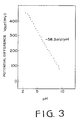
- Example 1 Using the redox membrane-coated carbon-sapphire electrode fabricated in Example 1, the relationship between the electromotive force produced across this electrode and a reference electrode (an Ag/AgCl electrode) and a change in pH in a phosphate buffer solution was determined. As a result, a linear relationship was found over a wide pH range of pH 1.0 - 9.0, and the slope of the straight line was 58 - 59 mV/pH (25 o C), thus substantially approximating the Nernst theoretical equation.
- a reference electrode an Ag/AgCl electrode
- the speed of response was substantially the same as that of a redox membrane-coated carbon electrode (coated wire-type electrode), namely 5 - 30 sec (pH range of pH 5 - 9).
- a semiconductor substrate silicon or sapphire
- a stable carbon thin membrane could be coated with a stable carbon thin membrane.
- Redox membrane-coated, carbon-membrane silicon substrate electrodes were fabricated under the same conditions as set forth in Example 1.
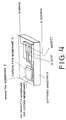
- a FET electrode 10 was prepared by coating the gate insulator of a MOSFET with a carbon thin membrane, and coating the latter with a polymeric membrane of 2,6 xylenol (set forth in Example 1) as an organic thin membrane by means of an electrolytic polymerization process.
- Numeral 1a denotes a drain diffusion area, 1b a drain electrode, 2a a source diffusion area, 2b a source electrode, 3 the polymeric membrane of 2,6 xylenol, 4 the carbon thin membrane, 5 a silicon nitride membrane, 6 a silicon oxide membrane, 7 p-type silicon, and 8 sapphire.
- the emf developed by the FET electrode 10 thus prepared was measured with respect to the pH of a liquid specimen 12 using the measurement apparatus shown in Fig. 2.
- the MOSFET characteristics (I D - V GS and I D - V DS ) of the FET sensors are the characteristics peculiar to the respective FET's.
- the present embodiment has been described with regard to the integrated-type FET electrode shown in Fig. 1, the same results can be obtained even with an isolated gate-type FET electrode of the kind shown in Fig. 4. The same results can also be obtained using a p-type silicon substrate or an n-type silicon substrate as the substrate.
- the specific resistance of the carbon-coated sapphire substrate is less than 10 ⁇ cm, particularly less than 1 ⁇ cm and, most preferred over all, less than 1 x 10 ⁇ 3 ⁇ cm, as illustrated in the present embodiment.
- the FET electrode can be used as a biosensor, such as an ion-selective FET sensor, a gas sensor for oxygen or the like and an enzyme sensor, by coating the organic thin membrane (3) of the FET electrode of the present embodiment with an ion-selective membrane (21) (a neutral carrier membrane), an oxygen-active membrane or further an enzyme-fixed membrane, etc.
- a biosensor such as an ion-selective FET sensor, a gas sensor for oxygen or the like and an enzyme sensor
Landscapes
- Life Sciences & Earth Sciences (AREA)
- Chemical & Material Sciences (AREA)
- Health & Medical Sciences (AREA)
- Physics & Mathematics (AREA)
- Biochemistry (AREA)
- Pathology (AREA)
- Chemical Kinetics & Catalysis (AREA)
- Electrochemistry (AREA)
- Immunology (AREA)
- Analytical Chemistry (AREA)
- Molecular Biology (AREA)
- General Health & Medical Sciences (AREA)
- General Physics & Mathematics (AREA)
- Engineering & Computer Science (AREA)
- Microelectronics & Electronic Packaging (AREA)
- Investigating Or Analyzing Materials By The Use Of Electric Means (AREA)
- Thin Film Transistor (AREA)
Abstract
Claims (5)
- Electrode à transistor à effet de champ (FET) comprenant un FET, caractérisée en ce qu'elle comprend en outre :
une membrane mince de carbone (4) revêtant un isolant de grille dudit FET, et
une membrane organique mince (3) revêtant ladite membrane mince de carbone. - Electrode à transistor à effet de champ (FET) selon la revendication 1, où la membrane mince de carbone (4) possède une résistance spécifique inférieure à 10 Ω.cm lorsqu'elle est appliquée à l'isolant de grille.
- Electrode à transistor à effet de champ (FET) selon la revendication 1, où la membrane organique (3) est une membrane qui présente une réponse d'oxydoréduction.
- Electrode à transistor à effet de champ (FET) selon la revendication 1, où il est en outre prévu une membrane sélective vis-à-vis d'ions qui revêt la membrane organique mince (3), si bien qu'il est constitué un capteur FET sélectif vis-à-vis d'ions.
- Electrode à transistor à effet de champ (FET) selon la revendication 4, où il est en outre prévu une membrane à enzymes fixées revêtant la membrane sélective vis-à-vis d'ions, si bien qu'il est constitué un capteur enzymatique permettant de mesurer la concentration d'un substrat biologique.
Applications Claiming Priority (3)
| Application Number | Priority Date | Filing Date | Title |
|---|---|---|---|
| JP275250/86 | 1986-11-20 | ||
| JP61275250A JPS63131056A (ja) | 1986-11-20 | 1986-11-20 | Fet電極 |
| PCT/JP1987/000900 WO1988004049A1 (fr) | 1986-11-20 | 1987-11-19 | Electrode a transistor a effet de champ (fet) |
Publications (3)
| Publication Number | Publication Date |
|---|---|
| EP0345347A1 EP0345347A1 (fr) | 1989-12-13 |
| EP0345347A4 EP0345347A4 (en) | 1991-01-09 |
| EP0345347B1 true EP0345347B1 (fr) | 1994-04-06 |
Family
ID=17552786
Family Applications (1)
| Application Number | Title | Priority Date | Filing Date |
|---|---|---|---|
| EP87907678A Expired - Lifetime EP0345347B1 (fr) | 1986-11-20 | 1987-11-19 | Electrode a transistor a effet de champ (fet) |
Country Status (7)
| Country | Link |
|---|---|
| US (1) | US5061976A (fr) |
| EP (1) | EP0345347B1 (fr) |
| JP (1) | JPS63131056A (fr) |
| KR (1) | KR900005618B1 (fr) |
| DE (1) | DE3789554T2 (fr) |
| DK (1) | DK403288A (fr) |
| WO (1) | WO1988004049A1 (fr) |
Families Citing this family (13)
| Publication number | Priority date | Publication date | Assignee | Title |
|---|---|---|---|---|
| JPH0743339B2 (ja) * | 1987-07-09 | 1995-05-15 | テルモ株式会社 | イオンセンサ |
| JPH0743342B2 (ja) * | 1987-09-21 | 1995-05-15 | テルモ株式会社 | リチウムイオンセンサ |
| JPH02296141A (ja) * | 1989-05-10 | 1990-12-06 | Terumo Corp | 機能性素子及びそれを備えたfetセンサ |
| US5938917A (en) * | 1995-04-05 | 1999-08-17 | The Regents Of The University Of California | Electrodes for measurement of peroxides |
| GB9705278D0 (en) * | 1997-03-14 | 1997-04-30 | Aromascan Plc | Gas sensor |
| DE19856294A1 (de) * | 1998-02-27 | 1999-09-09 | Fraunhofer Ges Forschung | Chemischer Feldeffekttransistor und Verfahren zu seiner Herstellung |
| KR100366705B1 (ko) * | 2000-05-26 | 2003-01-09 | 삼성에스디아이 주식회사 | 전기 화학 중합을 이용한 탄소나노튜브 에미터 제조 방법 |
| TW465055B (en) | 2000-07-20 | 2001-11-21 | Univ Nat Yunlin Sci & Tech | Method and apparatus for measurement of temperature parameter of ISFET using amorphous silicon hydride as sensor membrane |
| TW544752B (en) * | 2002-05-20 | 2003-08-01 | Univ Nat Yunlin Sci & Tech | Method for producing SnO2 gate ion sensitive field effect transistor (ISFET), and method and device for measuring the temperature parameters, drift and hysteresis values thereof |
| TWI241020B (en) * | 2004-03-31 | 2005-10-01 | Univ Nat Yunlin Sci & Tech | Method of manufacturing TiO2 sensing film, ISFET having TiO2 sensing film, and methods and apparatus for measuring the temperature parameter, drift, and hysteresis thereof |
| TWI295729B (en) * | 2005-11-01 | 2008-04-11 | Univ Nat Yunlin Sci & Tech | Preparation of a ph sensor, the prepared ph sensor, systems comprising the same, and measurement using the systems |
| DE102012105283A1 (de) * | 2011-06-24 | 2012-12-27 | Endress + Hauser Conducta Gesellschaft für Mess- und Regeltechnik mbH + Co. KG | Messaufnehmer zur Bestimmung einer einen Gehalt von H+- und/oder OH--Ionen in einem Messmedium repräsentierenden Messgröße |
| US8969154B2 (en) * | 2011-08-23 | 2015-03-03 | Micron Technology, Inc. | Methods for fabricating semiconductor device structures and arrays of vertical transistor devices |
Family Cites Families (42)
| Publication number | Priority date | Publication date | Assignee | Title |
|---|---|---|---|---|
| SU89314A1 (ru) * | 1949-04-23 | 1949-11-30 | П.Я. Мельников | Приспособление дл разравнивани штукатурного намета |
| US3598713A (en) * | 1969-06-03 | 1971-08-10 | Corning Glass Works | Potassium ion sensitive electrode |
| US3926764A (en) * | 1971-05-19 | 1975-12-16 | Radiometer As | Electrode for potentiometric measurements |
| GB1437091A (en) * | 1972-10-02 | 1976-05-26 | Radiometer As | Calcium electrode and membrane and composition for use therein |
| US3957612A (en) * | 1974-07-24 | 1976-05-18 | General Electric Company | In vivo specific ion sensor |
| US4115209A (en) * | 1974-10-30 | 1978-09-19 | Research Corporation | Method of determining ion activity using coated ion selective electrodes |
| US3957613A (en) * | 1974-11-01 | 1976-05-18 | General Electric Company | Miniature probe having multifunctional electrodes for sensing ions and gases |
| US4052285A (en) * | 1975-03-20 | 1977-10-04 | National Research Development Corporation | Ion selective electrodes |
| JPS5230490A (en) * | 1975-09-03 | 1977-03-08 | Denki Kagaku Keiki Co Ltd | Gas concentration measuring electrode stable in air |
| US4280889A (en) * | 1976-03-11 | 1981-07-28 | Honeywell Inc. | Solid state ion responsive and reference electrodes |
| US4214968A (en) * | 1978-04-05 | 1980-07-29 | Eastman Kodak Company | Ion-selective electrode |
| US4198851A (en) * | 1978-05-22 | 1980-04-22 | University Of Utah | Method and structure for detecting the concentration of oxygen in a substance |
| JPS5626250A (en) * | 1979-08-10 | 1981-03-13 | Olympus Optical Co Ltd | Composite chemical sensor |
| US4282079A (en) * | 1980-02-13 | 1981-08-04 | Eastman Kodak Company | Planar glass ion-selective electrode |
| JPS5763444A (en) * | 1980-10-02 | 1982-04-16 | Kuraray Co Ltd | Fet sensor with organic polymer film |
| JPS57118153A (en) * | 1981-01-14 | 1982-07-22 | Terumo Corp | Ph sensor |
| JPS57142356U (fr) * | 1981-02-28 | 1982-09-07 | ||
| US4563263A (en) * | 1982-01-15 | 1986-01-07 | Terumo Corporation | Selectively permeable film and ion sensor |
| DK158244C (da) * | 1982-03-15 | 1990-09-10 | Radiometer As | Ionselektiv maaleelektrode og fremgangsmaade til fremstilling af denne elektrode |
| JPS58167951A (ja) * | 1982-03-29 | 1983-10-04 | Hitachi Ltd | 塩素イオンセンサ |
| JPS5917662A (ja) * | 1982-07-21 | 1984-01-28 | Sharp Corp | 電子式キヤツシユレジスタ |
| JPS59102154A (ja) * | 1982-12-06 | 1984-06-13 | Olympus Optical Co Ltd | 化学的感応素子 |
| US4454007A (en) * | 1983-01-27 | 1984-06-12 | E. I. Du Pont De Nemours And Company | Ion-selective layered sensor and methods of making and using the same |
| JPS59164952A (ja) * | 1983-03-11 | 1984-09-18 | Hitachi Ltd | Fetイオンセンサ |
| JPS59176662A (ja) * | 1983-03-25 | 1984-10-06 | Sumitomo Electric Ind Ltd | 半導体センサ |
| US4561962A (en) * | 1983-04-06 | 1985-12-31 | Fluilogic Systems Oy | Ion-selective electrode and procedure for manufacturing same |
| JPS6052759A (ja) * | 1983-08-31 | 1985-03-26 | Terumo Corp | 酸素センサ− |
| JPS6073351A (ja) * | 1983-09-30 | 1985-04-25 | Hitachi Ltd | Fet化学センサ用素子 |
| NL8400916A (nl) * | 1984-03-22 | 1985-10-16 | Stichting Ct Voor Micro Elektr | Werkwijze voor het vervaardigen van een isfet en een aldus vervaardigde isfet. |
| JPS6111652A (ja) * | 1984-06-27 | 1986-01-20 | Sumitomo Electric Ind Ltd | 電界効果型半導体センサ |
| US4549951A (en) * | 1984-09-11 | 1985-10-29 | Sentech Medical Corporation | Ion selective electrode |
| US4615954A (en) * | 1984-09-27 | 1986-10-07 | Eltech Systems Corporation | Fast response, high rate, gas diffusion electrode and method of making same |
| DE3585915T2 (de) * | 1984-12-28 | 1993-04-15 | Terumo Corp | Ionensensor. |
| JPS61155949A (ja) * | 1984-12-28 | 1986-07-15 | Terumo Corp | pHセンサ− |
| KR900008847B1 (ko) * | 1985-05-27 | 1990-11-30 | 테루모가부시끼가이샤 | 이온센서 및 그 제조방법 |
| DK626986A (da) * | 1985-12-25 | 1987-06-26 | Terumo Corp | Ionsensor |
| DE3687123T2 (de) * | 1986-01-24 | 1993-05-13 | Terumo Corp | Ionenempfindlicher fet-fuehler. |
| JPS62180263A (ja) * | 1986-02-04 | 1987-08-07 | Terumo Corp | 酸素センサ− |
| JPS62277547A (ja) * | 1986-05-26 | 1987-12-02 | Terumo Corp | ガスセンサ− |
| CA1315927C (fr) * | 1986-12-10 | 1993-04-13 | Terumo Kabushiki Kaisha | Membrane ionique et chambre d'ionisation comportant cette membrane |
| JPH02296141A (ja) * | 1989-05-10 | 1990-12-06 | Terumo Corp | 機能性素子及びそれを備えたfetセンサ |
| JP2614002B2 (ja) * | 1992-07-06 | 1997-05-28 | 株式会社日本触媒 | 剥離性基材の製造方法 |
-
1986
- 1986-11-20 JP JP61275250A patent/JPS63131056A/ja active Pending
-
1987
- 1987-11-19 WO PCT/JP1987/000900 patent/WO1988004049A1/fr not_active Ceased
- 1987-11-19 US US07/687,214 patent/US5061976A/en not_active Expired - Lifetime
- 1987-11-19 KR KR1019880700857A patent/KR900005618B1/ko not_active Expired
- 1987-11-19 EP EP87907678A patent/EP0345347B1/fr not_active Expired - Lifetime
- 1987-11-19 DE DE3789554T patent/DE3789554T2/de not_active Expired - Fee Related
-
1988
- 1988-07-19 DK DK403288A patent/DK403288A/da not_active Application Discontinuation
Also Published As
| Publication number | Publication date |
|---|---|
| DE3789554T2 (de) | 1994-08-18 |
| US5061976A (en) | 1991-10-29 |
| WO1988004049A1 (fr) | 1988-06-02 |
| DK403288D0 (da) | 1988-07-19 |
| DE3789554D1 (de) | 1994-05-11 |
| EP0345347A1 (fr) | 1989-12-13 |
| KR900005618B1 (ko) | 1990-07-31 |
| KR890700226A (ko) | 1989-03-10 |
| EP0345347A4 (en) | 1991-01-09 |
| JPS63131056A (ja) | 1988-06-03 |
| DK403288A (da) | 1988-07-19 |
Similar Documents
| Publication | Publication Date | Title |
|---|---|---|
| Gernet et al. | Fabrication and characterization of a planar electrochemical cell and its application as a glucose sensor | |
| US7727370B2 (en) | Reference pH sensor, preparation and application thereof | |
| EP0345347B1 (fr) | Electrode a transistor a effet de champ (fet) | |
| US5716506A (en) | Electrochemical sensors for gas detection | |
| Yin et al. | Study of indium tin oxide thin film for separative extended gate ISFET | |
| EP0333860B1 (fr) | Capteur enzymatique | |
| Janata | Potentiometric microsensors | |
| Song et al. | Cl− sensitive biosensor used electrolyte-solution-gate diamond FETs | |
| Sohn et al. | ISFET glucose and sucrose sensors by using platinum electrode and photo-crosslinkable polymers | |
| Poghossian | Method of fabrication of ISFET-based biosensors on an Si–SiO2–Si structure | |
| US20040035699A1 (en) | Method and fabrication of the potentiometric chemical sensor and biosensor based on an uninsulated solid material | |
| EP0223597A2 (fr) | Compensation du tampon dans des appareils sensibles aux ions, modifiés enzymatiquement | |
| Shintani et al. | Polycrystalline boron-doped diamond with an oxygen-terminated surface channel as an electrolyte-solution-gate field-effect transistor for pH sensing | |
| US4716448A (en) | CHEMFET operation without a reference electrode | |
| US20090266712A1 (en) | Calcium ion sensors and fabrication method thereof, and sensing systems comprising the same | |
| JP3390756B2 (ja) | 電界効果トランジスタ | |
| JPH03131749A (ja) | 水素ガスセンサ | |
| EP0241991A2 (fr) | Transistor à effet de champ ayant une membrane par-dessus l'isolant de porte | |
| Hendrikse et al. | The EMOSFET as a potentiometric transducer in an oxygen sensor | |
| Bezegh et al. | Equilibrium fluctuation analysis of potassium ferro/ferricyanide redox system on platinum disk microelectrodes using field effect transistors | |
| JPH02249962A (ja) | Fetセンサ | |
| EP0304947A2 (fr) | Biosenseur | |
| Oyama et al. | A solid-state reference electrode based on bilayer coating with poly (p, p′-biphenol) and polyimide films for the gate of field effect transistor | |
| Lee et al. | Comparison of carbon and platinum performance as TiO2 membrane substrate material and applied to glucose biosensor using amperometric readout circuit | |
| Li et al. | Graphene-based ion-sensitive field effect transistor |
Legal Events
| Date | Code | Title | Description |
|---|---|---|---|
| PUAI | Public reference made under article 153(3) epc to a published international application that has entered the european phase |
Free format text: ORIGINAL CODE: 0009012 |
|
| AK | Designated contracting states |
Kind code of ref document: A1 Designated state(s): DE FR GB IT NL SE |
|
| 17P | Request for examination filed |
Effective date: 19890519 |
|
| A4 | Supplementary search report drawn up and despatched |
Effective date: 19901122 |
|
| AK | Designated contracting states |
Kind code of ref document: A4 Designated state(s): DE FR GB IT NL SE |
|
| 17Q | First examination report despatched |
Effective date: 19920813 |
|
| GRAA | (expected) grant |
Free format text: ORIGINAL CODE: 0009210 |
|
| AK | Designated contracting states |
Kind code of ref document: B1 Designated state(s): DE FR GB IT NL SE |
|
| PG25 | Lapsed in a contracting state [announced via postgrant information from national office to epo] |
Ref country code: SE Free format text: THE PATENT HAS BEEN ANNULLED BY A DECISION OF A NATIONAL AUTHORITY Effective date: 19940406 Ref country code: NL Effective date: 19940406 |
|
| REF | Corresponds to: |
Ref document number: 3789554 Country of ref document: DE Date of ref document: 19940511 |
|
| ITF | It: translation for a ep patent filed | ||
| ET | Fr: translation filed | ||
| NLV1 | Nl: lapsed or annulled due to failure to fulfill the requirements of art. 29p and 29m of the patents act | ||
| PG25 | Lapsed in a contracting state [announced via postgrant information from national office to epo] |
Ref country code: GB Effective date: 19941119 |
|
| PLBE | No opposition filed within time limit |
Free format text: ORIGINAL CODE: 0009261 |
|
| STAA | Information on the status of an ep patent application or granted ep patent |
Free format text: STATUS: NO OPPOSITION FILED WITHIN TIME LIMIT |
|
| 26N | No opposition filed | ||
| GBPC | Gb: european patent ceased through non-payment of renewal fee |
Effective date: 19941119 |
|
| PGFP | Annual fee paid to national office [announced via postgrant information from national office to epo] |
Ref country code: FR Payment date: 20021108 Year of fee payment: 16 |
|
| PGFP | Annual fee paid to national office [announced via postgrant information from national office to epo] |
Ref country code: DE Payment date: 20021121 Year of fee payment: 16 |
|
| PG25 | Lapsed in a contracting state [announced via postgrant information from national office to epo] |
Ref country code: DE Free format text: LAPSE BECAUSE OF NON-PAYMENT OF DUE FEES Effective date: 20040602 |
|
| PG25 | Lapsed in a contracting state [announced via postgrant information from national office to epo] |
Ref country code: FR Free format text: LAPSE BECAUSE OF NON-PAYMENT OF DUE FEES Effective date: 20040730 |
|
| REG | Reference to a national code |
Ref country code: FR Ref legal event code: ST |
|
| PG25 | Lapsed in a contracting state [announced via postgrant information from national office to epo] |
Ref country code: IT Free format text: LAPSE BECAUSE OF NON-PAYMENT OF DUE FEES;WARNING: LAPSES OF ITALIAN PATENTS WITH EFFECTIVE DATE BEFORE 2007 MAY HAVE OCCURRED AT ANY TIME BEFORE 2007. THE CORRECT EFFECTIVE DATE MAY BE DIFFERENT FROM THE ONE RECORDED. Effective date: 20051119 |