EP0345443A2 - Procédé de traitement thermique rapide d'une plaquette semi-conductrice par irradiation - Google Patents
Procédé de traitement thermique rapide d'une plaquette semi-conductrice par irradiation Download PDFInfo
- Publication number
- EP0345443A2 EP0345443A2 EP89106877A EP89106877A EP0345443A2 EP 0345443 A2 EP0345443 A2 EP 0345443A2 EP 89106877 A EP89106877 A EP 89106877A EP 89106877 A EP89106877 A EP 89106877A EP 0345443 A2 EP0345443 A2 EP 0345443A2
- Authority
- EP
- European Patent Office
- Prior art keywords
- semiconductor wafer
- radiation
- edge
- edge region
- intensity
- Prior art date
- Legal status (The legal status is an assumption and is not a legal conclusion. Google has not performed a legal analysis and makes no representation as to the accuracy of the status listed.)
- Granted
Links
Images




Classifications
-
- H—ELECTRICITY
- H10—SEMICONDUCTOR DEVICES; ELECTRIC SOLID-STATE DEVICES NOT OTHERWISE PROVIDED FOR
- H10P—GENERIC PROCESSES OR APPARATUS FOR THE MANUFACTURE OR TREATMENT OF DEVICES COVERED BY CLASS H10
- H10P34/00—Irradiation with electromagnetic or particle radiation of wafers, substrates or parts of devices
- H10P34/40—Irradiation with electromagnetic or particle radiation of wafers, substrates or parts of devices with high-energy radiation
- H10P34/42—Irradiation with electromagnetic or particle radiation of wafers, substrates or parts of devices with high-energy radiation with electromagnetic radiation, e.g. laser annealing
- H10P34/422—Irradiation with electromagnetic or particle radiation of wafers, substrates or parts of devices with high-energy radiation with electromagnetic radiation, e.g. laser annealing using incoherent radiation
-
- Y—GENERAL TAGGING OF NEW TECHNOLOGICAL DEVELOPMENTS; GENERAL TAGGING OF CROSS-SECTIONAL TECHNOLOGIES SPANNING OVER SEVERAL SECTIONS OF THE IPC; TECHNICAL SUBJECTS COVERED BY FORMER USPC CROSS-REFERENCE ART COLLECTIONS [XRACs] AND DIGESTS
- Y10—TECHNICAL SUBJECTS COVERED BY FORMER USPC
- Y10S—TECHNICAL SUBJECTS COVERED BY FORMER USPC CROSS-REFERENCE ART COLLECTIONS [XRACs] AND DIGESTS
- Y10S148/00—Metal treatment
- Y10S148/004—Annealing, incoherent light
Definitions
- the invention relates to a method for short-term tempering of a semiconductor wafer by electromagnetic radiation with a main radiation arrangement which has at least one radiation source and transmits the majority of the energy required for heating the semiconductor wafer.
- Rapid thermal processing is becoming increasingly important in the manufacture of electronic components on semiconductor wafers.
- the semiconductor wafers are brought individually into a process chamber and then heated very quickly and as evenly as possible in a defined atmosphere, for. B. by irradiation from an intense light source.
- the temperature is generally measured using a pyrometer at a measuring point in the center of the pane.
- the pyrometer signal regulates the power of the lamps and thus the light intensity in such a way that a given temperature-time cycle is adhered to as precisely as possible.
- a typical temperature-time cycle for healing ion implantations is e.g. a heating rate of 300 ° C per second to 1100 ° C, a subsequent annealing time of 5 seconds to 1100 ° C and a cooling rate of 100 ° C per second.
- a prerequisite for achieving high yields in short-term tempering processes is a sufficiently homogeneous temperature distribution over the semiconductor wafer.
- this requirement represents a problem that has not yet been satisfactorily solved, particularly in the case of large semiconductor wafer diameters.
- FIG. 1 shows a semiconductor wafer 1, the upper side 2 of which is completely chig is irradiated with electromagnetic radiation 3 of the same intensity.
- the heat radiation 4 which occurs in an increased manner at the semiconductor wafer edge 5
- a lower temperature is established at the semiconductor wafer edge 5 than in the middle of the semiconductor wafer 6.
- FIG. 3 shows a semiconductor wafer 1, the edge region 5 of which is irradiated with increased intensity in comparison to the semiconductor wafer center 6.
- the intensity distribution of the radiation is indicated schematically by arrows of different widths. Methods based on this principle are used to improve the temperature distribution in the known RTP systems, for example from Varian GmbH, D-7000 Stuttgart-Vaihingen, brochure no. VAC 6057 and Peak Systems, ING. Fremont, USA, ALP 6000, May 1986.
- the ratio of the intensity I M in the middle of the semiconductor wafer 6 to the intensity I R at the edge of the semiconductor wafer 5 is constant during the entire annealing process.
- the irradiation power is regulated by pyrometer measurements in the semiconductor wafer center 6 in such a way that a predetermined temperature-time cycle T M (t) in the wafer center 6 is maintained.
- T M temperature-time cycle
- the temperature at the semiconductor wafer edge 5 is significantly higher because of the higher heating rate there. It is only during the tempering phase t2 that, due to the constant intensity ratio I M / I R designed for this purpose, a homogeneous temperature distribution with the setpoint T S occurs after some time. During the cooling phase t3 after the irradiation has been switched off, the semiconductor wafer edge 5 then cools down faster than the semiconductor wafer center 6.
- the temperature-time profile T R (t) at the semiconductor wafer edge 5 therefore differs from the temperature-time profile T M (t) of the semiconductor wafer center 6 because of this dynamic behavior.
- the time until the homogeneous temperature distribution in the stationary one is reached Temper phase from the mass of the semiconductor wafer and the amount of the target temperature T S. It is z. B. for a semiconductor wafer with a diameter of 6 inches at a target temperature T S of 1100 ° C for five to ten seconds.
- regions on the semiconductor wafer edge 5 can experience on average a temperature which is up to 50 ° C. higher than regions in the semiconductor wafer center 6. This difference is all the more significant the shorter the annealing times.
- the object of the invention is therefore to provide a method for the short-term annealing of a semiconductor wafer by irradiation, which enables annealing processes with a homogeneous temperature distribution over the semiconductor wafer during the entire annealing process.
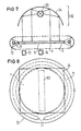
- FIGS. 6, 7, 9, 10, 11 show arrangements for carrying out the method according to the invention, FIGS. 6, 7, 9, 10, 11 being sectional views with a sectional plane perpendicular to the surface of the semiconductor wafer and FIG. 8 showing an arrangement in plan view.
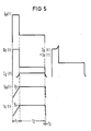
- an annealing process with a short heating-up time t 1, an annealing time t 2, during which the semiconductor wafer is to have a constant temperature, and a cooling time t 3 is considered.
- the top of the semiconductor wafer is irradiated over the entire area by a main irradiation arrangement.
- the intensity I M in the area of the center of the semiconductor wafer is equal to the intensity I R in the area of the edge of the semiconductor wafer.
- an electromagnetic radiation is additionally directed onto the edge region of the semiconductor wafer, the intensity of which I Z is changed over time so that the temperature T R in the region of the semiconductor wafer edge is equal to the temperature T M im during the entire tempering process Area of the semiconductor wafer center is.
- the course of the intensity I Z of the additional radiation is dependent on the course of the intensities I M , I R of the main radiation arrangement.
- the radiation intensities I M , I R and I Z can be kept constant in order to have the same constant set temperature T S in the range of To get the semiconductor wafer center and in the area of the semiconductor wafer edge.
- the additional irradiation I Z must start at a lower temperature than with a high heating-up speed, since, due to the longer heating-up time, the temperature inhomogeneity caused by the heat radiation at the edge of the semiconductor wafer is already formed at lower temperatures.
- a comparison of the radiation intensity I M of the radiation in the region of the semiconductor wafer center and the total radiation intensity I R + I Z in the region of the semiconductor wafer edge shows that the relative intensity distribution of the electromagnetic radiation over the semiconductor wafer is varied over time in the method according to the invention.
- the curves shown in the FIG apply to a typical tempering cycle with a heating rate of 300 ° C per second to 1100 ° C, a tempering time of 5 seconds at 1100 ° C and a cooling phase due to natural heat radiation.
- a reflection screen 61 can be arranged around the edge of the semiconductor wafer 1 in such a way that the heat radiation from the semiconductor wafer edge 5 is reflected back onto the latter.
- the heat radiation at the semiconductor wafer edge 5 is thus self-regulating at all times.
- the reflective screen 61 made of a highly reflective material can be made of metal, for example.
- An arc discharge lamp can be used as the main irradiation arrangement 62 63 serve, over which a curved reflector 64 is arranged, which is dimensioned such that the top of the semiconductor wafer 1 is irradiated over the entire area with the same intensity.
- the arrows indicate the radiation path schematically.
- the arrangement has an annular light source 71 arranged around the edge 5 of the semiconductor wafer 1 and having a reflector 72 with a parabolic cross section surrounding the annular light source 71.
- the regulation of the intensities I M and I R of the main irradiation arrangement 62 and the control of the intensity I Z of the annular light source 71 are carried out by means of temperature measurements in the area of the semiconductor wafer center and in the area of the semiconductor wafer edge.
- the intensity I Z of the irradiation of the light source 71 is regulated on the basis of the temperature differences determined in the semiconductor wafer center 6 and on the semiconductor wafer edge 5.
- the temperature measurements can be carried out, for example, by means of pyrometers 73, 74, which are suitable for the temperature ranges in question and, due to the contactless measuring principle, protect the sensitive semiconductor wafer 1.
- FIG. 7 The arrangement in FIG. 7 is shown again in a top view.
- the ring-shaped light source 71 e.g. a tungsten lamp, and the reflector with a parabolic cross section 72 are arranged concentrically around the edge 5 of the semiconductor wafer 1.
- an annular heating radiator 91 can be arranged around the edge of the semiconductor wafer 1, which can contain silicon carbide, for example, which has a silicon-like emissivity.
- the regulation of the intensity I Z of the additional Irradiation takes place, as described with reference to FIG. 7, by means of pyrometer measurements in the area of the semiconductor wafer center 6 and in the area of the semiconductor wafer edge 5.
- the time-dependent adjustment of the intensity I Z of the additional irradiation it is provided to change the distance of the ring-shaped radiant heater 91 to the semiconductor wafer 1 by moving the radiant heater 91 perpendicular to the semiconductor wafer surface (indicated by the double arrows).
- the main irradiation arrangement 62 is the same as that described with reference to FIG. 6.
- the main irradiation arrangement 62 is an irradiation source 103, 63 with a reflector 101, 111 above the semiconductor wafer 1, which is designed in such a way that the upper side at a certain distance of the semiconductor wafer 1 from the reflector 101, 111 the semiconductor wafer is irradiated over the entire area with the same intensity I M , I R.
- the semiconductor wafer 1 is movable, for example by quartz pins 102.
- the reflector 101, 111 is designed such that when the distance of the semiconductor wafer 1 from the radiation source 103, 63 is changed in a certain direction, the radiation striking the edge region of the semiconductor wafer 1 has a greater intensity than the radiation striking the central region of the semiconductor wafer .
- the movement of the semiconductor wafer 1 (indicated by the double arrows) can therefore compensate for the increased heat radiation occurring in the edge region of the semiconductor wafer 1.
- the movement of the semiconductor wafer 1 is controlled by means of pyrometer measurements, as described with reference to FIG. 7.
- a reflection chamber 101 can be used as the reflector, which completely encloses the semiconductor wafer 1 and the radiation source consisting of a plurality of light sources 103, for example tungsten lamps.
- a single radiation source 63 with a curved reflector 111 spanning the radiation source 63 and the semiconductor wafer 1 can also be used as the main radiation arrangement, the dimensions of which are designed such that a corresponding distance-dependent intensity distribution of the radiation is achieved.
- the invention also includes methods in which the bottom or top and bottom of the semiconductor wafer are irradiated by a main irradiation arrangement.
- the intensity I Z of the additional radiation can also be controlled on the basis of pre-calculated curves of the required intensity values.
- the method according to the invention can be used at all temperatures and can also be used in multi-stage tempering cycles.
Landscapes
- Radiation Pyrometers (AREA)
- Control Of Resistance Heating (AREA)
- Recrystallisation Techniques (AREA)
- Testing Or Measuring Of Semiconductors Or The Like (AREA)
Applications Claiming Priority (2)
| Application Number | Priority Date | Filing Date | Title |
|---|---|---|---|
| DE3815836 | 1988-05-09 | ||
| DE3815836 | 1988-05-09 |
Publications (3)
| Publication Number | Publication Date |
|---|---|
| EP0345443A2 true EP0345443A2 (fr) | 1989-12-13 |
| EP0345443A3 EP0345443A3 (en) | 1990-03-28 |
| EP0345443B1 EP0345443B1 (fr) | 1995-10-25 |
Family
ID=6354003
Family Applications (1)
| Application Number | Title | Priority Date | Filing Date |
|---|---|---|---|
| EP89106877A Expired - Lifetime EP0345443B1 (fr) | 1988-05-09 | 1989-04-17 | Procédé de traitement thermique rapide d'une plaquette semi-conductrice par irradiation |
Country Status (4)
| Country | Link |
|---|---|
| US (1) | US4981815A (fr) |
| EP (1) | EP0345443B1 (fr) |
| JP (1) | JP2961123B2 (fr) |
| DE (1) | DE58909475D1 (fr) |
Cited By (1)
| Publication number | Priority date | Publication date | Assignee | Title |
|---|---|---|---|---|
| DE4109956A1 (de) * | 1991-03-26 | 1992-10-01 | Siemens Ag | Verfahren zum kurzzeittempern einer halbleiterscheibe durch bestrahlung |
Families Citing this family (43)
| Publication number | Priority date | Publication date | Assignee | Title |
|---|---|---|---|---|
| US5179677A (en) * | 1990-08-16 | 1993-01-12 | Applied Materials, Inc. | Apparatus and method for substrate heating utilizing various infrared means to achieve uniform intensity |
| US5198371A (en) * | 1990-09-24 | 1993-03-30 | Biota Corp. | Method of making silicon material with enhanced surface mobility by hydrogen ion implantation |
| JP2780866B2 (ja) * | 1990-10-11 | 1998-07-30 | 大日本スクリーン製造 株式会社 | 光照射加熱基板の温度測定装置 |
| JPH04152518A (ja) * | 1990-10-16 | 1992-05-26 | Toshiba Corp | 半導体装置の製造方法 |
| US5192802A (en) * | 1991-09-25 | 1993-03-09 | Mcneil-Ppc, Inc. | Bioadhesive pharmaceutical carrier |
| US5215588A (en) * | 1992-01-17 | 1993-06-01 | Amtech Systems, Inc. | Photo-CVD system |
| US5229304A (en) * | 1992-05-04 | 1993-07-20 | At&T Bell Laboratories | Method for manufacturing a semiconductor device, including optical inspection |
| US5418885A (en) * | 1992-12-29 | 1995-05-23 | North Carolina State University | Three-zone rapid thermal processing system utilizing wafer edge heating means |
| US5395794A (en) * | 1993-04-22 | 1995-03-07 | Sklyarevich; Vladislav E. | Method of treating semiconductor materials |
| KR100297282B1 (ko) * | 1993-08-11 | 2001-10-24 | 마쓰바 구니유키 | 열처리장치 및 열처리방법 |
| US5467220A (en) * | 1994-02-18 | 1995-11-14 | Applied Materials, Inc. | Method and apparatus for improving semiconductor wafer surface temperature uniformity |
| US5561735A (en) * | 1994-08-30 | 1996-10-01 | Vortek Industries Ltd. | Rapid thermal processing apparatus and method |
| US5930586A (en) * | 1997-07-03 | 1999-07-27 | Motorola, Inc. | Method and apparatus for in-line measuring backside wafer-level contamination of a semiconductor wafer |
| US5960158A (en) * | 1997-07-11 | 1999-09-28 | Ag Associates | Apparatus and method for filtering light in a thermal processing chamber |
| US6080965A (en) * | 1997-09-18 | 2000-06-27 | Tokyo Electron Limited | Single-substrate-heat-treatment apparatus in semiconductor processing system |
| US5930456A (en) * | 1998-05-14 | 1999-07-27 | Ag Associates | Heating device for semiconductor wafers |
| US5970214A (en) * | 1998-05-14 | 1999-10-19 | Ag Associates | Heating device for semiconductor wafers |
| US6210484B1 (en) | 1998-09-09 | 2001-04-03 | Steag Rtp Systems, Inc. | Heating device containing a multi-lamp cone for heating semiconductor wafers |
| US6771895B2 (en) * | 1999-01-06 | 2004-08-03 | Mattson Technology, Inc. | Heating device for heating semiconductor wafers in thermal processing chambers |
| US6174388B1 (en) | 1999-03-15 | 2001-01-16 | Lockheed Martin Energy Research Corp. | Rapid infrared heating of a surface |
| US6303411B1 (en) | 1999-05-03 | 2001-10-16 | Vortek Industries Ltd. | Spatially resolved temperature measurement and irradiance control |
| US6403923B1 (en) | 1999-09-03 | 2002-06-11 | Mattson Technology, Inc. | System for controlling the temperature of a reflective substrate during rapid heating |
| US6359263B2 (en) | 1999-09-03 | 2002-03-19 | Steag Rtp Systems, Inc. | System for controlling the temperature of a reflective substrate during rapid heating |
| DE19952017A1 (de) * | 1999-10-28 | 2001-05-17 | Steag Rtp Systems Gmbh | Verfahren und Vorrichtung zum thermischen Behandeln von Substraten |
| US6259072B1 (en) | 1999-11-09 | 2001-07-10 | Axcelis Technologies, Inc. | Zone controlled radiant heating system utilizing focused reflector |
| US6353210B1 (en) | 2000-04-11 | 2002-03-05 | Applied Materials Inc. | Correction of wafer temperature drift in a plasma reactor based upon continuous wafer temperature measurements using and in-situ wafer temperature optical probe |
| US6423605B1 (en) * | 2000-11-09 | 2002-07-23 | Gyrotron Technology, Inc. | Method and apparatus for forming ultra-shallow junction for semiconductor device |
| US6594446B2 (en) * | 2000-12-04 | 2003-07-15 | Vortek Industries Ltd. | Heat-treating methods and systems |
| KR100443122B1 (ko) | 2001-10-19 | 2004-08-04 | 삼성전자주식회사 | 반도체 소자 제조장치용 히터 어셈블리 |
| US7445382B2 (en) * | 2001-12-26 | 2008-11-04 | Mattson Technology Canada, Inc. | Temperature measurement and heat-treating methods and system |
| AU2003287837A1 (en) | 2002-12-20 | 2004-07-14 | Vortek Industries Ltd | Methods and systems for supporting a workpiece and for heat-treating the workpiece |
| JP4557503B2 (ja) * | 2003-05-14 | 2010-10-06 | 株式会社東芝 | 半導体装置の製造方法及び半導体装置の製造装置 |
| JP5630935B2 (ja) * | 2003-12-19 | 2014-11-26 | マトソン テクノロジー、インコーポレイテッド | 工作物の熱誘起運動を抑制する機器及び装置 |
| TWI249588B (en) * | 2004-08-11 | 2006-02-21 | Ind Tech Res Inst | One kind of cavity apparatus of energy wave reflection device |
| US7184657B1 (en) | 2005-09-17 | 2007-02-27 | Mattson Technology, Inc. | Enhanced rapid thermal processing apparatus and method |
| US7133604B1 (en) | 2005-10-20 | 2006-11-07 | Bergstein David M | Infrared air heater with multiple light sources and reflective enclosure |
| JP5967859B2 (ja) * | 2006-11-15 | 2016-08-10 | マトソン テクノロジー、インコーポレイテッド | 熱処理中の被加工物を支持するシステムおよび方法 |
| DE102007058002B4 (de) * | 2007-12-03 | 2016-03-17 | Mattson Thermal Products Gmbh | Vorrichtung zum thermischen Behandeln von scheibenförmigen Halbleitersubstraten |
| WO2009137940A1 (fr) | 2008-05-16 | 2009-11-19 | Mattson Technology Canada, Inc. | Procédé et appareil de prévention de rupture de pièce ouvrée |
| US8404048B2 (en) * | 2011-03-11 | 2013-03-26 | Applied Materials, Inc. | Off-angled heating of the underside of a substrate using a lamp assembly |
| WO2014035957A1 (fr) * | 2012-08-30 | 2014-03-06 | Applied Materials, Inc. | Anneaux de dépôt réfléchissants et chambres de traitement de substrat les incorporant |
| KR20170043936A (ko) * | 2015-10-14 | 2017-04-24 | 현대자동차주식회사 | 블랭크 가열 장치 |
| CN111071501B (zh) * | 2019-12-31 | 2021-04-20 | 中国科学院力学研究所 | 一种真空环境下模态试验结构温度补偿器 |
Family Cites Families (24)
| Publication number | Priority date | Publication date | Assignee | Title |
|---|---|---|---|---|
| US3627590A (en) * | 1968-12-02 | 1971-12-14 | Western Electric Co | Method for heat treatment of workpieces |
| US3763348A (en) * | 1972-01-05 | 1973-10-02 | Argus Eng Co | Apparatus and method for uniform illumination of a surface |
| US4115163A (en) * | 1976-01-08 | 1978-09-19 | Yulia Ivanovna Gorina | Method of growing epitaxial semiconductor films utilizing radiant heating |
| SE7710800L (sv) * | 1976-10-05 | 1978-04-06 | Western Electric Co | Forfarande for astadkommande av ett epitaxiellt skikt pa ett substrat |
| US4101759A (en) * | 1976-10-26 | 1978-07-18 | General Electric Company | Semiconductor body heater |
| GB2060998B (en) * | 1979-10-17 | 1983-12-14 | Itt Ind Ltd | Semiconductor annealing |
| JPS56100412A (en) * | 1979-12-17 | 1981-08-12 | Sony Corp | Manufacture of semiconductor device |
| JPS56100426A (en) * | 1980-01-14 | 1981-08-12 | Ushio Inc | Device and method for annealing |
| JPS5750427A (en) * | 1980-09-12 | 1982-03-24 | Ushio Inc | Annealing device and annealing method |
| JPS5764937A (en) * | 1980-10-09 | 1982-04-20 | Ushio Inc | Annealing device |
| JPS5764936A (en) * | 1980-10-09 | 1982-04-20 | Ushio Inc | Annealing device |
| US4469529A (en) * | 1981-12-04 | 1984-09-04 | Ushio Denki Kabushiki Kaisha | Method for heating semiconductor wafer by means of application of radiated light with supplemental circumferential heating |
| US4468259A (en) * | 1981-12-04 | 1984-08-28 | Ushio Denki Kabushiki Kaisha | Uniform wafer heating by controlling light source and circumferential heating of wafer |
| JPS58135630A (ja) * | 1982-02-08 | 1983-08-12 | Fujitsu Ltd | 半導体層のアニ−ル方法 |
| JPS5959876A (ja) * | 1982-09-30 | 1984-04-05 | Ushio Inc | 光照射炉の運転方法 |
| JPS5977289A (ja) * | 1982-10-26 | 1984-05-02 | ウシオ電機株式会社 | 光照射炉 |
| JPS6032317A (ja) * | 1983-08-03 | 1985-02-19 | Hitachi Ltd | 半導体ウエハの熱処理方法および熱処理装置 |
| JPS60247934A (ja) * | 1984-05-23 | 1985-12-07 | Hitachi Ltd | 熱処理装置 |
| JPS6130239U (ja) * | 1984-07-27 | 1986-02-24 | ニチデン機械株式会社 | 赤外線加熱装置 |
| JPS61289620A (ja) * | 1985-06-18 | 1986-12-19 | Sony Corp | 半導体薄膜の熱処理方法 |
| JPS6220308A (ja) * | 1985-07-19 | 1987-01-28 | Hitachi Ltd | 熱処理方法および装置 |
| JPS6246516A (ja) * | 1985-08-26 | 1987-02-28 | Hitachi Ltd | 熱処理装置 |
| JPS62293622A (ja) * | 1986-06-12 | 1987-12-21 | Kokusai Electric Co Ltd | 半導体基板の熱処理装置 |
| US4888302A (en) * | 1987-11-25 | 1989-12-19 | North American Philips Corporation | Method of reduced stress recrystallization |
-
1989
- 1989-03-13 US US07/322,113 patent/US4981815A/en not_active Expired - Fee Related
- 1989-04-17 DE DE58909475T patent/DE58909475D1/de not_active Expired - Fee Related
- 1989-04-17 EP EP89106877A patent/EP0345443B1/fr not_active Expired - Lifetime
- 1989-05-02 JP JP1113545A patent/JP2961123B2/ja not_active Expired - Fee Related
Cited By (3)
| Publication number | Priority date | Publication date | Assignee | Title |
|---|---|---|---|---|
| DE4109956A1 (de) * | 1991-03-26 | 1992-10-01 | Siemens Ag | Verfahren zum kurzzeittempern einer halbleiterscheibe durch bestrahlung |
| US5399523A (en) * | 1991-03-26 | 1995-03-21 | Siemens Aktiengesellscaft | Method for the rapid thermal processing of a semiconductor wafer by irradiation |
| EP0505928B1 (fr) * | 1991-03-26 | 2002-06-12 | Infineon Technologies AG | Procédé de traitement thermique rapide d'une plaquette semi-conductrice par irradiation |
Also Published As
| Publication number | Publication date |
|---|---|
| EP0345443A3 (en) | 1990-03-28 |
| DE58909475D1 (de) | 1995-11-30 |
| US4981815A (en) | 1991-01-01 |
| JP2961123B2 (ja) | 1999-10-12 |
| EP0345443B1 (fr) | 1995-10-25 |
| JPH01319934A (ja) | 1989-12-26 |
Similar Documents
| Publication | Publication Date | Title |
|---|---|---|
| EP0345443B1 (fr) | Procédé de traitement thermique rapide d'une plaquette semi-conductrice par irradiation | |
| DE102008062494B4 (de) | Vorrichtung zur Erwärmung von Substraten sowie Verfahren zur Erwärmung von Substraten | |
| EP0505928B1 (fr) | Procédé de traitement thermique rapide d'une plaquette semi-conductrice par irradiation | |
| DE3852642T2 (de) | Heizsystem für reaktionskammer einer chemischen dampfniederschlagsvorrichtung. | |
| DE69816913T2 (de) | Anlage zur Temperaturreglung der Seitenwände eines Ofens | |
| DE2412102C2 (de) | Verfahren und Vorrichtung zum Herstellen einer dotierten Halbleiterzone und einer ohmschen Kontaktdoppelschicht hierauf | |
| DE3688422T2 (de) | Beheizung eines fliessbettofens. | |
| DE69118228T2 (de) | Klemmechanismus für physikalische Dampfniederschlagvorrichtung | |
| DE2102115A1 (de) | Verfahren und Vorrichtung zum Aus gleichen einer durch Wärmeeinwirkung be dingten Linsenwirkung in einem Lasersvstem | |
| DE112019001415B4 (de) | Trägerplatte für eine lokale Erwärmung in thermischen Verarbeitungssystemen | |
| DE602004007756T2 (de) | Ein Lichtbestrahlungsverfahren und ein Lichtbestrahlungsapparat | |
| DE3216850C2 (fr) | ||
| DE102007058002B4 (de) | Vorrichtung zum thermischen Behandeln von scheibenförmigen Halbleitersubstraten | |
| DE4223133C2 (fr) | ||
| DE102018203945B4 (de) | Verfahren zur Herstellung von Halbleiterscheiben | |
| DE102004028714A1 (de) | Thermische Behandlungsvorrichtung | |
| EP1224688A1 (fr) | Procede et dispositif pour le traitement thermique de substrats | |
| DE3139712A1 (de) | Glueheinrichtung | |
| DE3139711A1 (de) | Glueheinrichtung | |
| DE4142466C2 (de) | Verfahren zur schnellen Abkühlung beim Kurzzeittempern einer Halbleiterscheibe | |
| EP3341973A1 (fr) | Procédé et dispositif pour stabiliser une cellule solaire photovoltaïque au silicium | |
| DE890055C (de) | Waermofen | |
| DE3904034C2 (fr) | ||
| DE102019106072B4 (de) | Verfahren zum Betreiben eines Infrarot-Heizstrahlers und Vorrichtung mit Infrarot-Heizstrahler | |
| DE3031087C2 (de) | Verfahren zur Einstellung der Temperatur eines Industrieofens |
Legal Events
| Date | Code | Title | Description |
|---|---|---|---|
| PUAI | Public reference made under article 153(3) epc to a published international application that has entered the european phase |
Free format text: ORIGINAL CODE: 0009012 |
|
| AK | Designated contracting states |
Kind code of ref document: A2 Designated state(s): CH DE FR GB IT LI NL |
|
| PUAL | Search report despatched |
Free format text: ORIGINAL CODE: 0009013 |
|
| AK | Designated contracting states |
Kind code of ref document: A3 Designated state(s): CH DE FR GB IT LI NL |
|
| 17P | Request for examination filed |
Effective date: 19900427 |
|
| 17Q | First examination report despatched |
Effective date: 19930528 |
|
| GRAA | (expected) grant |
Free format text: ORIGINAL CODE: 0009210 |
|
| AK | Designated contracting states |
Kind code of ref document: B1 Designated state(s): CH DE FR GB IT LI NL |
|
| REF | Corresponds to: |
Ref document number: 58909475 Country of ref document: DE Date of ref document: 19951130 |
|
| REG | Reference to a national code |
Ref country code: CH Ref legal event code: NV Representative=s name: SIEMENS-ALBIS AKTIENGESELLSCHAFT |
|
| ITF | It: translation for a ep patent filed | ||
| GBT | Gb: translation of ep patent filed (gb section 77(6)(a)/1977) |
Effective date: 19960108 |
|
| ET | Fr: translation filed | ||
| PLBE | No opposition filed within time limit |
Free format text: ORIGINAL CODE: 0009261 |
|
| STAA | Information on the status of an ep patent application or granted ep patent |
Free format text: STATUS: NO OPPOSITION FILED WITHIN TIME LIMIT |
|
| 26N | No opposition filed | ||
| REG | Reference to a national code |
Ref country code: GB Ref legal event code: IF02 |
|
| PGFP | Annual fee paid to national office [announced via postgrant information from national office to epo] |
Ref country code: IT Payment date: 20060430 Year of fee payment: 18 |
|
| PGFP | Annual fee paid to national office [announced via postgrant information from national office to epo] |
Ref country code: DE Payment date: 20060620 Year of fee payment: 18 |
|
| PGFP | Annual fee paid to national office [announced via postgrant information from national office to epo] |
Ref country code: NL Payment date: 20070413 Year of fee payment: 19 Ref country code: CH Payment date: 20070413 Year of fee payment: 19 |
|
| PGFP | Annual fee paid to national office [announced via postgrant information from national office to epo] |
Ref country code: GB Payment date: 20070426 Year of fee payment: 19 |
|
| PG25 | Lapsed in a contracting state [announced via postgrant information from national office to epo] |
Ref country code: DE Free format text: LAPSE BECAUSE OF NON-PAYMENT OF DUE FEES Effective date: 20071101 |
|
| PGFP | Annual fee paid to national office [announced via postgrant information from national office to epo] |
Ref country code: FR Payment date: 20070416 Year of fee payment: 19 |
|
| REG | Reference to a national code |
Ref country code: CH Ref legal event code: PL |
|
| GBPC | Gb: european patent ceased through non-payment of renewal fee |
Effective date: 20080417 |
|
| NLV4 | Nl: lapsed or anulled due to non-payment of the annual fee |
Effective date: 20081101 |
|
| PG25 | Lapsed in a contracting state [announced via postgrant information from national office to epo] |
Ref country code: LI Free format text: LAPSE BECAUSE OF NON-PAYMENT OF DUE FEES Effective date: 20080430 Ref country code: NL Free format text: LAPSE BECAUSE OF NON-PAYMENT OF DUE FEES Effective date: 20081101 Ref country code: CH Free format text: LAPSE BECAUSE OF NON-PAYMENT OF DUE FEES Effective date: 20080430 |
|
| REG | Reference to a national code |
Ref country code: FR Ref legal event code: ST Effective date: 20081231 |
|
| PG25 | Lapsed in a contracting state [announced via postgrant information from national office to epo] |
Ref country code: FR Free format text: LAPSE BECAUSE OF NON-PAYMENT OF DUE FEES Effective date: 20080430 |
|
| PG25 | Lapsed in a contracting state [announced via postgrant information from national office to epo] |
Ref country code: GB Free format text: LAPSE BECAUSE OF NON-PAYMENT OF DUE FEES Effective date: 20080417 |
|
| PG25 | Lapsed in a contracting state [announced via postgrant information from national office to epo] |
Ref country code: IT Free format text: LAPSE BECAUSE OF NON-PAYMENT OF DUE FEES Effective date: 20070417 |