EP0349207A2 - Opto-elektronische Interface-Einrichtung - Google Patents
Opto-elektronische Interface-Einrichtung Download PDFInfo
- Publication number
- EP0349207A2 EP0349207A2 EP89306349A EP89306349A EP0349207A2 EP 0349207 A2 EP0349207 A2 EP 0349207A2 EP 89306349 A EP89306349 A EP 89306349A EP 89306349 A EP89306349 A EP 89306349A EP 0349207 A2 EP0349207 A2 EP 0349207A2
- Authority
- EP
- European Patent Office
- Prior art keywords
- optical
- channel
- optical fiber
- printed circuit
- opto
- Prior art date
- Legal status (The legal status is an assumption and is not a legal conclusion. Google has not performed a legal analysis and makes no representation as to the accuracy of the status listed.)
- Granted
Links
Images





Classifications
-
- G—PHYSICS
- G02—OPTICS
- G02B—OPTICAL ELEMENTS, SYSTEMS OR APPARATUS
- G02B6/00—Light guides; Structural details of arrangements comprising light guides and other optical elements, e.g. couplings
- G02B6/24—Coupling light guides
- G02B6/42—Coupling light guides with opto-electronic elements
-
- G—PHYSICS
- G02—OPTICS
- G02B—OPTICAL ELEMENTS, SYSTEMS OR APPARATUS
- G02B6/00—Light guides; Structural details of arrangements comprising light guides and other optical elements, e.g. couplings
- G02B6/44—Mechanical structures for providing tensile strength and external protection for fibres, e.g. optical transmission cables
- G02B6/4439—Auxiliary devices
- G02B6/444—Systems or boxes with surplus lengths
- G02B6/4453—Cassettes
-
- G—PHYSICS
- G02—OPTICS
- G02B—OPTICAL ELEMENTS, SYSTEMS OR APPARATUS
- G02B6/00—Light guides; Structural details of arrangements comprising light guides and other optical elements, e.g. couplings
- G02B6/24—Coupling light guides
- G02B6/42—Coupling light guides with opto-electronic elements
- G02B6/4201—Packages, e.g. shape, construction, internal or external details
- G02B6/4246—Bidirectionally operating package structures
-
- G—PHYSICS
- G02—OPTICS
- G02B—OPTICAL ELEMENTS, SYSTEMS OR APPARATUS
- G02B6/00—Light guides; Structural details of arrangements comprising light guides and other optical elements, e.g. couplings
- G02B6/24—Coupling light guides
- G02B6/42—Coupling light guides with opto-electronic elements
- G02B6/4292—Coupling light guides with opto-electronic elements the light guide being disconnectable from the opto-electronic element, e.g. mutually self aligning arrangements
-
- G—PHYSICS
- G02—OPTICS
- G02B—OPTICAL ELEMENTS, SYSTEMS OR APPARATUS
- G02B6/00—Light guides; Structural details of arrangements comprising light guides and other optical elements, e.g. couplings
- G02B6/44—Mechanical structures for providing tensile strength and external protection for fibres, e.g. optical transmission cables
- G02B6/4439—Auxiliary devices
- G02B6/444—Systems or boxes with surplus lengths
- G02B6/4452—Distribution frames
- G02B6/44526—Panels or rackmounts covering a whole width of the frame or rack
-
- G—PHYSICS
- G02—OPTICS
- G02B—OPTICAL ELEMENTS, SYSTEMS OR APPARATUS
- G02B6/00—Light guides; Structural details of arrangements comprising light guides and other optical elements, e.g. couplings
- G02B6/44—Mechanical structures for providing tensile strength and external protection for fibres, e.g. optical transmission cables
- G02B6/4439—Auxiliary devices
- G02B6/444—Systems or boxes with surplus lengths
- G02B6/44528—Patch-cords; Connector arrangements in the system or in the box
Definitions
- the invention relates to electro-optical systems and, more particularly, to arrangements for interconnecting optical and opto-electronic devices on printed circuit cards.
- Opto-electronic termination equipment generally includes both electronic circuitry and an assembly of opto-electronic and optical devices interconnected by optical fibers.
- Optical fibers are usually small in diameter, brittle and have transmission characteristics that may be adversely affected by splicing and bending beyond a prescribed minimum bend radius. Consequently, it is necessary to use special handling techniques to assure reliable interconnection without impairment of the lightwave signals.
- the optical signal portion of termination equipment has generally been separated from the printed circuit cards on which the electrical termination functions are performed.
- the separation allows adequate space needed for assembly and repair of high quality optical interconnections without interfering with automatic assembly of electronic components on the printed circuit cards.
- the card must be adapted to accommodate optical fiber interconnections by special mounting arrangements for the opto-electronic devices and optical connectors.
- U. S. Patent 4,461,537 discloses an opto-electronic device incorporated in a fiber optic connector assembly that includes an optical port, an optical lens and means for guiding a fiber end into alignment with the lens mounted on a printed circuit board.
- the arrangement uses a simple optical fiber structure on the printed circuit card that is adjusted to an only single opto-electronic conversion.
- the connector assembly is not suitable for optical interconnections requiring a high degree of accuracy or for more complex optical interconnections such as used in communication systems.
- U.S. Patent 4,432,604 describes a self-adjusting fiber optic connector assembly having optical fibers extending therefrom to opto-electronic devices mounted on a printed circuit card wherein the optical fiber and electrical connections are made on the board.
- the self-adjusting connectors permit changes in placement of optical fibers on a printed circuit card but are not adapted to complex optical fiber arrangements and do not permit controlled looping of interconnecting optical fibers.
- a opto- electronic and optical devices are interconnected by optical fibers in a structure adapted for automatic insertion into an electronic circuit board.
- the invention is directed to an opto-electronic organizing arrangement having a closed loop trough for retaining optical fibers.
- a plurality of optical fibers are directed into the closed loop trough at different locations therealong.
- the optical fibers are selectively interconnected within the closed loop trough.
- the closed loop trough includes first and second portions and at least one optical fiber retaining channel which forms a passageway for optical fibers between the first and second portions to change the direction of optical fiber passing therethrough between clockwise and counter-clockwise directions.
- FIG. 1 shows a front perspective view of an optical organizer 40 affixed to a printed circuit card 10 that is illustrative of the invention.
- the assembly of the organizer and printed circuit card is adapted to perform opto-electronic conversions.
- printed circuit card 10 retains and interconnects electronic components which perform the electrical filtering, signal amplification and electrical and optical connections associated with opto-electronic coupling.
- Card 10 comprises electrical connection section 13, amplifier and driver section 16 for supplying electrical pulses to lightwave signal producing device 44, low level electronic receiver section 18 which receives electrical signals from lightwave to electrical signal conversion device 54, and receiver amplifier section 20.
- Optical organizer 40 retains and interconnects opto-electronic and optical components adapted to convert a lightwave signal obtained from a simultaneous two-way optical fiber transmission medium external to the card to an electrical signal and to convert an electrical signal from a source terminal to a lightwave signal for application to the simultaneous two way optical fiber transmission medium.
- the lightwave signal producing device 44 of FIG. 1 which may be a semiconductor laser is removably attached to optical organizer 40 by the clamping structure including clamp sections 51 and 52 adjacent to connector section 13.
- Device 44 has three electrical leads 47, 48 and 49 extending from one end bent at right angles for coupling to driver section 16 of the card and an output optical fiber 50 extending outward from its opposite end parallel to the adjacent surface of card 10.
- Lightwave to electrical converter 54 which may be a photoelectric device for lightwave signals is removably attached to organizer 40 by the clamp structure including clamp sections 60 and 61 adjacent to low level receiver section 18 of card 10.
- Photoelectric device 54 of FIG. 1 has three electrical leads 55, 56 and 57 extending from one end which are bent at right angles to connect to the input of receiver section 18 and has an input optical fiber 59 extending from the other end parallel to the adjacent surface of card 10.
- the optical portion of the optical coupler of FIG. 1 also includes optical fiber connection device 42 and optical splitter 70.
- the optical splitter which may for example be of the well known fuse tapered type, is operative as a directional coupler to couple incoming lightwave signals from a two way lightwave transmission channel to photoelectric device 54 via optical connection device 42 and to couple outgoing lightwave signals from semiconductor laser 44 to the lightwave transmission channel.
- Connector 42 couples lightwave signals received from the two way lightwave transmission channel to optical splitter 70 which then directs a portion of the received lightwave signals to photo conductor device 54 and directs lightwave signals generated in semiconductor laser 44 to the two way lightwave transmission channel by way of optical connection device 42.
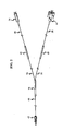
- FIG. 2 shows a perspective view of laser 44, photo-detector 54, connection device 42 and splitter 70 interconnected by optical fibers prior to insertion into organizer 40.
- Laser 44 has optical fiber 50 extending therefrom.
- Light detector 54 has optical fiber 59 extending therefrom. Each of these fibers has a length in the order of one meter.
- Optical splitter 70 has optical fibers 72 and 74 extending from one end and one optical fiber 64 extending from the opposite end. Each of the optical splitter fibers is also of the order of one meter in length.
- Optical fiber 64 is attached directly to connection device 42.
- Optical fiber 59 is interconnected with fiber 72 by splice device 62 while fiber 50 from semiconductor laser 44 is connected to fiber 74 from splitter 70 by splice device 65.
- the splice devices may be of the fusion or mechanical types. Since the transmission characteristics are dependent on the splicing interfaces between fibers, the relatively long lengths of optical fibers are needed to permit resplicing so that acceptable lightwave transmission characteristics are assured.
- the organizer of FIG. 1 accommodates the lengths of interconnecting optical fiber on the restricted area of the printed circuit card without interference with electrical components mounted on the card.
- FIG. 3 shows a front view of optical organizer 40 into which the portion of the assembly of FIG. 2 including optical connection device 42, optical splitter 70 and optical fiber 64 interconnecting the optical connection device and the optical splitter shown in FIG. 2 is inserted.
- the organizer comprises a closed trough loop around the printed circuit card edges and a straight trough section connecting opposite sides of the trough loop. Structures to hold the optical and opto-electronic devices connected by optical fiber are affixed to the trough loop and the traversing trough at predetermined positions so that electrical connections therefrom are aligned with prescribed positions in the printed circuit card.
- Two or more alignment pins e.g. 12 and 14 on the organizer are adapted for insertion into alignment apertures on the printed circuit card to automate the placement of the optical assembly on the printed circuit card.
- the trough loop includes upper channel 101, side channels 103 and 105 and lower channel 107.
- Cross channel 109 connects the middle portion of upper channel 101 to the middle portion of lower channel 107.
- Channel 110 extending from the right side of upper channel 101 includes a structure at the end thereof for retaining optical connection device 42 in a preassigned position at one end of the organizer.
- Cross channel 109 includes clamp elements 76, 77, 78 and 79 which hold optical splitter 70 in place so that optical fibers extending therefrom may be directed into upper channel 101 and lower channel 107.
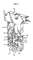
- the rectangular structure including bar member 112 extending downward from one side of channel 110 parallel to channel 103 and bar member 114 extending perpendicularly from side 115 of channel 103 is adapted to retain light transmitter device 44 by means of opposing clamping elements 51 and 52. Electrical leads 47, 48 and 49 from the transmitter device are inserted through apertures 117, 118 and 119 on bar 114 which apertures are aligned with corresponding apertures in the printed wiring pattern on card 10 shown in FIG. 1 during assembly of the organizer on the printed circuit card.
- transmitter device 44 and its heat sink block 43 are held in place between wall 115 of channel 103 and bar 112 by hook ended clamp elements 51 and 52.
- Clamp 51 is attached to bar 112 by ledge 108 on the rearward side of bar 112, and the clamp extends frontward along bar 112 to its hook shaped end.
- Clamp 52 is similarly attached to the outside of channel 103 by a ledge not shown and extends frontward parallel to the wall 115.
- leads 47, 48 and 49 are passed through apertures 117, 118 and 119, the assembled transmitter device 44 and its heat sink block 43 are inserted between clamp elements 51 and 52.
- These clamp elements are separated from bar 112 and the side of channel 103. They yield to allow passage of the transmitter device and heat sink assembly between bar 112 and wall 115 but return to clamp heat sink block 43 as shown in FIG. 7.
- Receiving device 54 is placed in a prescribed position by the retaining structure formed between bar 121, bar 123 extending from channel 101 and bar 125 extending from channel 105 in FIG. 3.
- Apertures 128, 129 and 130 in bar member 125 are adapted to receive electrical leads 55, 56 and 57 on receiving device 54.
- Apertures 128, 129 and 130 are located so that the receiving device leads are automatically inserted at the preassigned terminal holes of receiving circuit 18 on card 10 when the organizer and the card are brought into alignment.
- the receiving device retaining structure is shown in greater detail in FIG. 8. In FIG. 8, receiving device 54 is held in place between bars 121 and 123 by hook ended clamp elements 60 and 61.
- Clamp 61 is attached to bar 123 via bracket 81 and clamp 60 is similarly attached to bar 121 by a bracket (not shown).
- Clamp element 61 extends frontward from bracket 81 parallel to bar 123 and clamp element 60 extends frontward parallel to bar 121.
- leads 56, 57 and 58 are passed through apertures 128, 129 and 130, receiving device 54 is inserted between clamp elements 60 and 61. Since the clamp elements are spaced from bar 121 and bar 123, they yield to allow passage of the receiving device between bars 121 and 123 and return to hold the receiving device as shown in FIG. 8.
- the arrangement for retaining optical splitter 70 in its predetermined location is cross channel 109 is shown in greater detail in FIG. 6.
- opposing clamp elements 76 and 77 yield outwardly to receive one end portion of optical splitter 70 while opposing clamp elements 78 and 79 yield outwardly to receive the other end portion of the optical splitter.
- the two sets of opposing clamp elements partially enclose splitter 70 to affix the splitter in its predetermined location.
- Splitter 70 is positioned in the right portion of cross channel 109 so that a large section of the cross channel is open for passage therethrough of interconnecting optical fibers.
- Tab 91 extends over the fiber passageway in channel 109 whereby the interconnecting optical fiber passing through the channel is confined therein.
- Optical connection device 42 is positioned on organizer 40 by rectangular shaped retaining frame 132 as shown in FIG. 3.
- the retaining frame arrangement is shown in greater detail in FIG. 9.
- retaining frame 132 is affixed to the end of channel 110 remote from upper channel 101.
- the retaining frame has a U-shaped passageway therethrough which passageway receives optical connection device 42 from channel 110.
- Retaining clip 133 grips the retaining frame 132 to hold the device 42 firmly in its predetermined location.
- channels 101 and 103 are joined by curved channel section 142 which maintains a minimum radius of curvature of optical fiber passing therethrough.
- Curved channel section 150 restricts the radius of curvature of optical fibers at the intersection between channels 101 and 105.
- the intersections of channels 105 and 107, and channels 107 and 103 are joined by curved portions 152 and 153, respectively, so that the minimum radius of curvature of optical fibers is maintained.
- Cross channel 109 is joined to upper channel 101 by curved sides 151 and 155 and includes curved guides 144 and 145 so that optical fiber can be directed into channel 101 clockwise or counterclockwise within the minimum radius requirements.
- the intersection of channel 109 and lower channel 17 includes curved sides 158 and 159 and curved guides 147 and 148 to assure that optical fiber entering channel 107 from cross channel 109 do not violate the bend radius requirements.
- Organizer 40 is made of Polyethersulfone or other suitable material known in the art and sized to fit on printed circuit card so as not to interfere with the electrical circuit arrangements mounted on the printed circuit card and to align the electrical leads of the opto-electronic components with the printed wiring pattern of the printed circuit card.
- the requirements of the printed circuit card control the placement of the opto-electronic and optical devices on organizer 40 and the paths of the interconnecting optical fiber are adapted to conform to the location of these devices.
- Optical connection section 42 is placed at the electrical connection end of the organizer above electrical connection section 13 on FIG. 1 so that insertion and removal of the assembled printed circuit card does not require movement of the optical fiber transmission line and electrical and lightwave connections are made simultaneously at one end of the printed circuit card.
- Semiconductor laser 44 is mounted near the electrical connector end of the organizer, while photoconductor diode 54 is mounted on the opposite side of the organizer to minimize pickup by the photoconductor of high level electrical pulses applied to the laser.
- the locations of the semiconductor laser and the photoconductor diode are coordinated with the placement of electrical circuitry on the printed wiring card to provide appropriate electronic interfaces.
- organizer 40 includes an oval-shaped trough including channels 101, 103, 105 and 107 in which optical fibers can be directed either in the clockwise or counterclockwise direction.
- Cross channel 109 partitions the closed loop trough into two U shaped portions.
- channel 109 extending between upper channel 101 and lower channel 107 permits a clockwise or counterclockwise directed optical fiber entering cross channel 109 to exit the cross channel in either the clockwise or the counterclockwise direction.
- optical interconnections can be made independent of the placement or orientation of optical or opto-electronic devices.
- the channels of organizer 40 are open on one side to permit insertion of fiber and splicing devices therein.
- the height of the channel sides must at least accommodate the multiple loops of interconnecting optical fibers 50, 59, 64, 72 and 74 and fusion splicing devices 62 and 65 but not so large as to interfere with other apparatus used with the printed circuit card in the optical transmission terminal assembly. Since fusion splicing devices 62 and 65 have much larger cross-sections than either jacketed or unjacketed optical fibers, they are placed in channel portions having a minimum number of optical fibers therein. As aforementioned, fusion splicing device 65 is generally positioned in the left-hand portion of channel 101 as shown in FIG.
- fusion splicing device 62 is generally positioned in the left portion of channel 107 as shown in FIG. 5.
- the number of optical fibers traversing the portions of channels 101 and 107 having splicing devices therein is limited to provide space for the splicing devices while multiple turns of optical fibers 50, 59, 64, 72 and 74 are placed around the loop including the other portions of channels 101 and 107 and cross channel 109 which has no splicing devices.
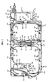
- FIG. 3 illustrates the placement of optical fiber 64 of the optical assembly of FIG. 2 into the organizer.
- Optical connection device 42 is first inserted into retaining frame structure 132.
- the unjacketed optical fiber 64 from optical connection device 42 enters channel 101 from channel extension 110, and one or more turns of the fiber are inserted counterclockwise into the loop including the U shaped portion formed by channel 101, channel 107 and channel 103 and cross channel 109.
- Optical fiber 64 from the connection device enters channel 109 from upper channel 101 between guides 144 and 145.
- Optical splitter 70 at the other end of fiber 64 is then clamped in place in cross channel 109 by clamp element pairs 76 and 77, and 78 and 79.
- optical splitter 70 is placed in cross channel 109 of the organizer, the portion of the optical assembly connecting optical splitter 70 with transmitter laser device 44 including unjacketed optical fiber 74, fusion splice 65 and jacketed fiber 50 interconnecting fusion splice 65 and laser device 44 is placed in the organizer as shown in FIG. 4.
- fiber 74 exiting cross channel 109 enters lower channel 107 between curved guides 147 and 148 and the outer wall of channel 107.
- Fiber 74 is wound counter clockwise one or more times around the loop including the right portion of channel 107, side channel 103, upper channel 101 and cross channel 109 and is retained under tabs 95, 97, 96 and 91.
- Fiber 74 enters channel 109 counterclockwise between curved guides 144 and 145.
- Fiber 74 is then inserted clockwise into the left portion of lower channel 107 to traverse the U shaped portion of the closed loop trough including the left portion lower channel 107, side channel 105 and the left portion of upper channel 101 so that fusion splice device 65 is placed in channel 101 underneath tab 92.
- fusion splice device 65 may be placed underneath tab 93 in side channel 105.
- the placement of the fusion splice device in either channel 101 or channel 105 is dependent on the length of fiber 74. In either location, it may be necessary to route fiber 74 differently so that the interconnection is maintained without excessive slack in the fiber. This is so because the length of fiber 74 depends on the point at which a successful splice is made.
- optical fiber 50 is inserted into upper channel 101 and directed around the loop including the U shaped portion formed by upper channel 101, side channel 103, lower channel 107 and cross channel 109 one or more times to exit upper channel 101 at channel extension 110.
- Transmitter device 44, at the other end of fiber 50, is then inserted into its retaining structure as previously described.
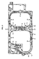
- optical fiber 72 between splitter 70 and fusion splice device 62, splice device 62 and fiber 59 interconnecting splice device 62, and receiver device 54 is inserted into the organizer so that fiber 72 enters lower channel 107 between guides 147 and 148 to run counter clockwise in the loop including channels 107, 103 and 101 and cross channel 109 one or more times as shown in FIG. 5.
- Fiber 72 then enters the left portion of upper channel 101, passes through side channel 105 into the left portion of lower channel 107 so that fusion splice 62 is placed in the left portion of channel 107 underneath tab 94.
- fiber 72 does not permit placement of splice device 62 underneath tab 94, it may be placed in side channel 105 underneath tab 93. A different routing of fiber 72 may be required depending on its length after the splices are made in the optical assembly shown in FIG. 2.
- optical fiber 59 extending from fusion splice device 62 is passed through to the right portion of lower channel 107 so that it traverses the loop including lower channel 107, side channel 103, upper channel 101 and cross channel 109 one or more times. Fiber 59 exits this loop at the left portion of upper channel 101 and receiver device 54 at the other end of fiber 59 is then inserted into its retaining structure on organizer 40 as previously described.
- the aforementioned method of placement of the optical assembly of FIG. 2 into organizer 40 is appropriate if the lengths of the optical fibers shown in FIG. 2 are not appreciably modified when the fibers are interconnected via fusion splice devices 62 and 65.
- optical fiber lengths may be changed significantly to obtain the desired light wave transmission characteristics by resplicing or to effect a repair or replacement of opto-electronic or optical components. If such changes in optical fiber lengths are made, the paths of the interconnecting optical fibers must be altered so that the opto-electronic and optical devices fit in their retaining structures.
- path alterations may include clockwise-to-counterclockwise and counterclockwise-to-clockwise direction changes in the fiber paths.
- the inclusion of at least one cross channel connecting the sections of the outer channel loop in accordance with the invention permits such direction alterations to be readily made.
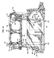
- FIG. 10 shows a perspective view of the component side of printed circuit board 10 and organizer 40 to illustrate the placement of the organizer on the printed circuit board.
- devices 42, 44, 54, and 70 of FIG. 1 are not shown in FIG. 10.
- electrical leads 47, 48 and 49 are positioned through apertures 117, 118 and 119, and electrical leads 55, 56 and 57 are positioned through apertures 128, 129 and 130 shown in FIG. 10.
- Alignment pin 12 extending from the outer sidewall of the right portion of channel 107 and alignment pin 14 extending from the outer sidewall of channel 110 are adapted to be inserted into alignment apertures 120 and 140, respectively, in printed circuit board 10.
- alignment pins 12 and 14 are placed in printed circuit board apertures 120 and 140, apertures 117, 118 and 119 are aligned with terminal board apertures 165, 166 and 167 and apertures 128, 129 and 130 are aligned with terminal board apertures 155, 156 and 157.
- Electrical leads 47, 48 and 49 extending through apertures 117, 118 and 119 and electrical leads 55, 56 and 57 extending through apertures 128, 129 and 130 are made shorter than alignment pins 12 and 14 so that insertion of the alignment pins assure placement of electrical leads 47, 48 and 49 into terminal board apertures 165, 166 and 167 and placement of electrical leads 55, 56 and 57 into terminal board apertures 155 156 and 157. Consequently, affixing organizer 40 to board 10 using the alignment arrangement shown in FIG. 10 automatically inserts the electrical leads of the opto-electronic devices in organizer 40 into the electrical circuitry of printed circuit board 10.
- the construction of the organizer in accordance with the invention permits automated assembly of the organizer and printed circuit card.
- Expansion type pin structures 170, 171, 172 and 173 on organizer 40 are adapted as is well known in the art to be inserted into apertures 180, 181, 182 and 183, respectively, in printed circuit card 10 to clamp the organizer in its aligned position to the printed circuit card.
Landscapes
- Physics & Mathematics (AREA)
- General Physics & Mathematics (AREA)
- Optics & Photonics (AREA)
- Optical Couplings Of Light Guides (AREA)
- Mechanical Coupling Of Light Guides (AREA)
- Light Guides In General And Applications Therefor (AREA)
Applications Claiming Priority (2)
| Application Number | Priority Date | Filing Date | Title |
|---|---|---|---|
| US07/213,003 US4861134A (en) | 1988-06-29 | 1988-06-29 | Opto-electronic and optical fiber interface arrangement |
| US213003 | 1988-06-29 |
Publications (3)
| Publication Number | Publication Date |
|---|---|
| EP0349207A2 true EP0349207A2 (de) | 1990-01-03 |
| EP0349207A3 EP0349207A3 (de) | 1992-04-01 |
| EP0349207B1 EP0349207B1 (de) | 1995-12-06 |
Family
ID=22793353
Family Applications (1)
| Application Number | Title | Priority Date | Filing Date |
|---|---|---|---|
| EP89306349A Expired - Lifetime EP0349207B1 (de) | 1988-06-29 | 1989-06-23 | Opto-elektronische Interface-Einrichtung |
Country Status (6)
| Country | Link |
|---|---|
| US (1) | US4861134A (de) |
| EP (1) | EP0349207B1 (de) |
| JP (1) | JP2634667B2 (de) |
| KR (1) | KR0181291B1 (de) |
| AU (1) | AU607619B2 (de) |
| CA (1) | CA1317365C (de) |
Cited By (9)
| Publication number | Priority date | Publication date | Assignee | Title |
|---|---|---|---|---|
| EP0533112A1 (de) * | 1991-09-19 | 1993-03-24 | Eastman Kodak Company | Verbesserte Lichtwellenleiter-Halterung und -Träger |
| EP0562290A1 (de) * | 1992-03-26 | 1993-09-29 | The Whitaker Corporation | Optische Sternkopplereinheit |
| EP0529559A3 (de) * | 1991-08-23 | 1994-01-05 | Eastman Kodak Co | |
| DE4221475A1 (de) * | 1992-06-30 | 1994-01-05 | Siemens Ag | Lichtwellenleiter-Spleißeinsatz für ein Endverzweigergehäuse |
| EP0595396A1 (de) * | 1992-10-30 | 1994-05-04 | PIRELLI CAVI S.p.A. | Ein kompakter optischer Verstärker |
| US5383051A (en) * | 1992-10-30 | 1995-01-17 | Pirelli Cavi S.P.A. | Compact-size optical amplifier |
| EP0875011A4 (de) * | 1995-12-22 | 1999-09-29 | Corning Inc | Optischer schaltkreis auf gedruckter leiterplatte |
| WO2000075707A1 (en) * | 1999-06-07 | 2000-12-14 | Ciena Corporation | Optical fiber management tool |
| US6868216B1 (en) | 2001-07-27 | 2005-03-15 | Ciena Corporation | Fiber optic cable management system |
Families Citing this family (104)
| Publication number | Priority date | Publication date | Assignee | Title |
|---|---|---|---|---|
| US5228105A (en) * | 1987-05-04 | 1993-07-13 | Glista Andrew S | Programmable electro-optic packaging and interconnect system |
| GB8827348D0 (en) * | 1988-11-23 | 1988-12-29 | British Telecomm | Fibre distribution arrangement |
| US5071211A (en) * | 1988-12-20 | 1991-12-10 | Northern Telecom Limited | Connector holders and distribution frame and connector holder assemblies for optical cable |
| US4995688A (en) * | 1989-07-31 | 1991-02-26 | Adc Telecommunications, Inc. | Optical fiber distribution frame |
| CH679612A5 (de) * | 1989-09-14 | 1992-03-13 | Asea Brown Boveri | |
| US5093885A (en) * | 1990-07-11 | 1992-03-03 | Adc Telecommunications, Inc. | Fiber optic connector module |
| US5179618A (en) * | 1990-07-11 | 1993-01-12 | Adc Telecommunications, Inc. | Fiber optic connector module |
| US5093887A (en) * | 1990-09-28 | 1992-03-03 | Reliance Comm/Tec Corporation | Sliding cable tray with cable pivot arm |
| USD330368S (en) | 1991-05-30 | 1992-10-20 | Northern Telecom Limited | Tray for housing splices and excess lengths of optical fibers |
| US5265186A (en) * | 1991-11-12 | 1993-11-23 | At&T Bell Laboratories | Optical fiber distribution apparatus |
| JPH05150120A (ja) * | 1991-11-29 | 1993-06-18 | Fujitsu Ltd | 光フアイバケーブルの導入構造 |
| IT1255953B (it) * | 1992-10-30 | 1995-11-17 | Pirelli Cavi Spa | Amplificatore ottico compatto a funzioni separate |
| US5363465A (en) * | 1993-02-19 | 1994-11-08 | Adc Telecommunications, Inc. | Fiber optic connector module |
| US5469526A (en) * | 1994-01-07 | 1995-11-21 | Porta Systems Corp. | Optical fiber support for printed circuit boards |
| GB9400626D0 (en) * | 1994-01-14 | 1994-03-09 | Augat Limited | Management of optical fibres |
| US5442726A (en) * | 1994-02-22 | 1995-08-15 | Hubbell Incorporated | Optical fiber storage system |
| US5461693A (en) | 1994-07-14 | 1995-10-24 | At&T Ipm Corp. | Optical fiber distribution frame with fiber testing |
| US5652820A (en) * | 1995-11-13 | 1997-07-29 | Act Communications, Inc. | Fiber optic splice closure and protection apparatus |
| JPH09211357A (ja) * | 1996-01-31 | 1997-08-15 | Asahi Optical Co Ltd | 走査光学装置における点光源列の角度調節機構及び調節方法 |
| US5740300A (en) * | 1996-05-01 | 1998-04-14 | Scientific-Atlanta, Inc. | Transceiver module support apparatus with fiber management features |
| US5712942A (en) * | 1996-05-13 | 1998-01-27 | Lucent Technologies Inc. | Optical communications system having distributed intelligence |
| JPH09304631A (ja) * | 1996-05-14 | 1997-11-28 | Japan Riicom:Kk | ケーブル接続用クロージャ |
| US6353183B1 (en) | 1996-05-23 | 2002-03-05 | The Siemon Company | Adapter plate for use with cable adapters |
| US5696864A (en) * | 1996-09-18 | 1997-12-09 | Communications Technology Corporation | Aerial enclosure for coupling data signals to a customer site |
| KR100242412B1 (ko) * | 1996-10-25 | 2000-03-02 | 윤종용 | 광섬유 증폭기의 광학소자 고정용 패키징 박스 |
| GB9703306D0 (en) * | 1997-02-18 | 1997-04-09 | Integrated Optical Components | Carriers for optical components and methods of using the same |
| US5943461A (en) * | 1997-05-12 | 1999-08-24 | Lucent Technologies Inc | Connectorized optical module package and method using same with internal fiber connections |
| US5907654A (en) * | 1997-08-13 | 1999-05-25 | Northern Telecom Limited | Printed circuit board for connection to an optical fiber |
| US6015239A (en) * | 1998-04-20 | 2000-01-18 | Cielo Communications, Inc. | Passively aligned opto-electronic coupling assembly |
| US6272276B1 (en) * | 1998-10-15 | 2001-08-07 | Lucent Technologies, Inc. | Device and method for retaining a laser module in an orientation suitable for testing and shipping |
| US6263143B1 (en) * | 1998-10-15 | 2001-07-17 | Lucent Technologies Inc. | Package housing for laser module wound on a spool |
| US6208797B1 (en) | 1998-10-30 | 2001-03-27 | Fujitsu Network Communications, Inc. | Optical fiber routing device and method of assembly therefor |
| US6418263B1 (en) * | 1999-01-28 | 2002-07-09 | Tyco Submarine Systems Ltd. | Method and apparatus for storing a fiber optic assembly |
| US6760531B1 (en) | 1999-03-01 | 2004-07-06 | Adc Telecommunications, Inc. | Optical fiber distribution frame with outside plant enclosure |
| US6347760B1 (en) | 1999-05-25 | 2002-02-19 | Tycom (Us) Inc. | Device for storing optical fibers |
| US6343761B1 (en) | 1999-05-25 | 2002-02-05 | Tycom (Us) Inc. | Device for separating portions of spooled optical fibers |
| US6367730B1 (en) | 1999-05-25 | 2002-04-09 | Tycom (Us) Inc. | Device for storing optical fibers |
| US6213651B1 (en) | 1999-05-26 | 2001-04-10 | E20 Communications, Inc. | Method and apparatus for vertical board construction of fiber optic transmitters, receivers and transceivers |
| US6901221B1 (en) | 1999-05-27 | 2005-05-31 | Jds Uniphase Corporation | Method and apparatus for improved optical elements for vertical PCB fiber optic modules |
| US7116912B2 (en) * | 1999-05-27 | 2006-10-03 | Jds Uniphase Corporation | Method and apparatus for pluggable fiber optic modules |
| US20010030789A1 (en) * | 1999-05-27 | 2001-10-18 | Wenbin Jiang | Method and apparatus for fiber optic modules |
| US6322019B1 (en) * | 1999-09-08 | 2001-11-27 | Tycom (Us) Inc. | Device for covering a jacketed fiber storage space |
| EP1255667A1 (de) * | 2000-02-07 | 2002-11-13 | Te Huruhuru Properties Ltd. | Transportabler schlepp-skilift |
| US6427045B1 (en) * | 2000-03-08 | 2002-07-30 | Marconi Communications, Inc. | Splice tray for use in splicing fiber optic cables and housing therefor |
| GB2368136B (en) * | 2000-10-17 | 2004-09-08 | Spirent Plc | Optical fibre splice storage tray |
| USD465455S1 (en) | 2000-12-11 | 2002-11-12 | Fiber Optic Network Solutions Corporation | Module for fiber optic equipment |
| US6901200B2 (en) | 2000-12-22 | 2005-05-31 | Fiber Optic Network Solutions, Inc. | Module and housing for optical fiber distribution and DWDM equipment |
| US6942395B1 (en) | 2001-01-29 | 2005-09-13 | Jds Uniphase Corporation | Method and apparatus of pull-lever release for fiber optic modules |
| US6846115B1 (en) | 2001-01-29 | 2005-01-25 | Jds Uniphase Corporation | Methods, apparatus, and systems of fiber optic modules, elastomeric connections, and retention mechanisms therefor |
| US6607308B2 (en) * | 2001-02-12 | 2003-08-19 | E20 Communications, Inc. | Fiber-optic modules with shielded housing/covers having mixed finger types |
| US6659655B2 (en) * | 2001-02-12 | 2003-12-09 | E20 Communications, Inc. | Fiber-optic modules with housing/shielding |
| US6863448B2 (en) | 2001-04-14 | 2005-03-08 | Jds Uniphase Corporation | Method and apparatus for push button release fiber optic modules |
| US6692159B2 (en) | 2001-04-14 | 2004-02-17 | E20 Communications, Inc. | De-latching mechanisms for fiber optic modules |
| US6796715B2 (en) | 2001-04-14 | 2004-09-28 | E20 Communications, Inc. | Fiber optic modules with pull-action de-latching mechanisms |
| US6840680B1 (en) | 2001-04-14 | 2005-01-11 | Jds Uniphase Corporation | Retention and release mechanisms for fiber optic modules |
| US6994478B1 (en) | 2001-04-14 | 2006-02-07 | Jds Uniphase Corporation | Modules having rotatable release and removal lever |
| US6851867B2 (en) | 2001-04-14 | 2005-02-08 | Jds Uniphase Corporation | Cam-follower release mechanism for fiber optic modules with side delatching mechanisms |
| JP2003149461A (ja) * | 2001-11-12 | 2003-05-21 | Allied Tereshisu Kk | 収納装置 |
| US20030219194A1 (en) * | 2002-04-19 | 2003-11-27 | Barthel William F. | Optical fiber management system and method |
| US6829425B2 (en) | 2002-04-19 | 2004-12-07 | Plexus Corporation | Optical fiber management system and method |
| US6741785B2 (en) | 2002-04-19 | 2004-05-25 | Plexus Corporation | Optical fiber management system and method |
| US7118281B2 (en) | 2002-08-09 | 2006-10-10 | Jds Uniphase Corporation | Retention and release mechanisms for fiber optic modules |
| US7142764B2 (en) | 2003-03-20 | 2006-11-28 | Tyco Electronics Corporation | Optical fiber interconnect cabinets, termination modules and fiber connectivity management for the same |
| US7198409B2 (en) | 2003-06-30 | 2007-04-03 | Adc Telecommunications, Inc. | Fiber optic connector holder and method |
| US7233731B2 (en) | 2003-07-02 | 2007-06-19 | Adc Telecommunications, Inc. | Telecommunications connection cabinet |
| US7239789B2 (en) * | 2003-10-06 | 2007-07-03 | Preformed Line Products Company | Optical fiber splice case |
| US7369741B2 (en) | 2003-11-17 | 2008-05-06 | Fiber Optics Network Solutions Corp. | Storage adapter with dust cap posts |
| US6983095B2 (en) * | 2003-11-17 | 2006-01-03 | Fiber Optic Network Solutions Corporation | Systems and methods for managing optical fibers and components within an enclosure in an optical communications network |
| US7331722B2 (en) * | 2004-05-05 | 2008-02-19 | Avago Technologies Fiber Ip Pte Ltd | Optical module for housing an optical component |
| US7218827B2 (en) | 2004-06-18 | 2007-05-15 | Adc Telecommunications, Inc. | Multi-position fiber optic connector holder and method |
| US7194181B2 (en) | 2005-03-31 | 2007-03-20 | Adc Telecommunications, Inc. | Adapter block including connector storage |
| US7623749B2 (en) | 2005-08-30 | 2009-11-24 | Adc Telecommunications, Inc. | Fiber distribution hub with modular termination blocks |
| US7885504B2 (en) * | 2005-12-16 | 2011-02-08 | Fci Americas Technology, Inc. | Dual-optical fiber coupler enclosure |
| US7816602B2 (en) | 2006-02-13 | 2010-10-19 | Adc Telecommunications, Inc. | Fiber distribution hub with outside accessible grounding terminals |
| US7720343B2 (en) | 2006-02-13 | 2010-05-18 | Adc Telecommunications, Inc. | Fiber distribution hub with swing frame and modular termination panels |
| US7760984B2 (en) | 2006-05-04 | 2010-07-20 | Adc Telecommunications, Inc. | Fiber distribution hub with swing frame and wrap-around doors |
| US8229265B2 (en) | 2007-11-21 | 2012-07-24 | Adc Telecommunications, Inc. | Fiber distribution hub with multiple configurations |
| JP5176722B2 (ja) * | 2008-06-30 | 2013-04-03 | 富士通株式会社 | 光部品ユニットの製造方法、および、光部品ユニット |
| US8382382B2 (en) | 2008-08-27 | 2013-02-26 | Adc Telecommunications, Inc. | Fiber optic adapter with integrally molded ferrule alignment structure |
| MX2011005380A (es) | 2008-11-21 | 2011-06-06 | Adc Telecommunications Inc | Modulo de telecomunicaciones de fibra optica. |
| CN101852898B (zh) * | 2009-03-30 | 2014-03-12 | 日立电线株式会社 | 光连接器及使用了光连接器的光纤模块 |
| JP5445278B2 (ja) * | 2009-10-29 | 2014-03-19 | 住友電気工業株式会社 | 光通信モジュール、及びその製造方法 |
| US8376634B2 (en) * | 2009-10-29 | 2013-02-19 | Sumitomo Electric Industries, Ltd. | Pluggable optical transceiver and method for manufacturing the same |
| US9052477B2 (en) | 2009-10-29 | 2015-06-09 | Sumitomo Electric Industries, Ltd. | Optical transceiver with inner fiber set within tray securing thermal path from electronic device to housing |
| US8821039B2 (en) | 2009-10-29 | 2014-09-02 | Sumitomo Electric Industries, Ltd. | Optical transceiver having optical receptacle arranged diagonally to longitudinal axis |
| CN102830471B (zh) * | 2009-10-29 | 2015-03-25 | 住友电气工业株式会社 | 可插式光收发器及其制造方法 |
| US8958679B2 (en) | 2010-03-02 | 2015-02-17 | Tyco Electronics Services Gmbh | Fibre-optic telecommunications module |
| US9417418B2 (en) | 2011-09-12 | 2016-08-16 | Commscope Technologies Llc | Flexible lensed optical interconnect device for signal distribution |
| CN103917904A (zh) | 2011-10-07 | 2014-07-09 | Adc电信公司 | 光纤盒、系统和方法 |
| US9001862B2 (en) * | 2012-03-09 | 2015-04-07 | Raytheon Company | Miniaturized solid-state lasing device, system and method |
| US9146362B2 (en) | 2012-09-21 | 2015-09-29 | Adc Telecommunications, Inc. | Insertion and removal tool for a fiber optic ferrule alignment sleeve |
| ES2792122T3 (es) | 2012-09-28 | 2020-11-10 | Commscope Connectivity Uk Ltd | Casete de fibra óptica |
| US9146374B2 (en) | 2012-09-28 | 2015-09-29 | Adc Telecommunications, Inc. | Rapid deployment packaging for optical fiber |
| US9223094B2 (en) | 2012-10-05 | 2015-12-29 | Tyco Electronics Nederland Bv | Flexible optical circuit, cassettes, and methods |
| GB2507741A (en) * | 2012-11-07 | 2014-05-14 | Bombardier Transp Gmbh | Cable bearing element for inductive power coupling |
| US9435975B2 (en) | 2013-03-15 | 2016-09-06 | Commscope Technologies Llc | Modular high density telecommunications frame and chassis system |
| EP3100090A4 (de) | 2014-01-28 | 2017-09-06 | ADC Telecommunications Inc. | Verschiebbares glasfaser-verbindungsmodul mit kabelüberlängenverwaltung |
| US9494758B2 (en) | 2014-04-03 | 2016-11-15 | Commscope Technologies Llc | Fiber optic distribution system |
| WO2016066614A1 (en) * | 2014-10-27 | 2016-05-06 | Commscope Emea Limited | Splice module for fiber blade |
| WO2016184363A1 (zh) | 2015-05-15 | 2016-11-24 | 爱德奇电讯国际贸易(上海)有限公司 | 对准套管组件和光纤适配器 |
| EP3163341A1 (de) | 2015-10-27 | 2017-05-03 | CCS Technology, Inc. | Verteilungspunkteinheit zum koppeln externer elektrischer und optischer kabel |
| EP3692404A4 (de) | 2017-10-02 | 2021-06-16 | Commscope Technologies LLC | Faseroptische schaltung und herstellungsverfahren |
| JP6956131B2 (ja) * | 2019-03-28 | 2021-10-27 | 株式会社豊田自動織機 | スクロール型圧縮機 |
| EP4127799B1 (de) | 2020-03-31 | 2025-11-19 | CommScope Technologies LLC | Glasfaserkabelverwaltungssysteme |
Family Cites Families (29)
| Publication number | Priority date | Publication date | Assignee | Title |
|---|---|---|---|---|
| US4217030A (en) * | 1978-07-18 | 1980-08-12 | Bell Telephone Laboratories, Incorporated | Fiberoptic-electronic connector assembly |
| NL7900432A (nl) * | 1979-01-19 | 1980-07-22 | Nkf Groep Bv | Glasvezel verbindingsmof. |
| US4266853A (en) * | 1979-03-12 | 1981-05-12 | Northern Telecom Limited | Device for organizing optical fibers and the like |
| US4294512A (en) * | 1980-01-14 | 1981-10-13 | Thomas & Betts Corporation | Optoelectronic interface apparatus |
| US4360729A (en) * | 1980-11-17 | 1982-11-23 | Geosource Inc. | Seismic cable connector with optical transceiver |
| US4428645A (en) * | 1981-01-28 | 1984-01-31 | Gk Technologies, Incorporated | Cable accumulator |
| US4461537A (en) * | 1981-12-24 | 1984-07-24 | Molex Incorporated | Fiber optic connector assembly |
| FR2524987A1 (fr) * | 1982-04-09 | 1983-10-14 | Cables De Lyon Geoffroy Delore | Dispositif de raccordement des extremites de deux cables sous-marins a fibres optiques et son procede de fabrication |
| US4432604A (en) * | 1982-04-28 | 1984-02-21 | Bell Telephone Laboratories, Incorporated | Self-adjusting fiberoptic connector assembly |
| JPS599311U (ja) * | 1982-07-12 | 1984-01-21 | 古河電気工業株式会社 | 光ケ−ブル接続箱 |
| FR2531576A1 (fr) * | 1982-08-04 | 1984-02-10 | Cit Alcatel | Bati de raccordement et d'interface opto-electronique |
| FR2538918A1 (fr) * | 1983-01-05 | 1984-07-06 | Telecommunications Sa | Boite de raccordement et de brassage pour fibres optiques |
| JPS60107806U (ja) * | 1983-12-19 | 1985-07-22 | 古河電気工業株式会社 | 光フアイバスプライスケ−ス |
| JPS60189283A (ja) * | 1984-03-09 | 1985-09-26 | Hitachi Ltd | 光電子装置 |
| US4702551A (en) * | 1984-10-11 | 1987-10-27 | Reliance Comm/Tec Corporation | Method and apparatus for handling and storing cabled spliced ends of fiber optics |
| GB8426008D0 (en) * | 1984-10-15 | 1984-11-21 | Telephone Cables Ltd | Optical communication systems |
| FR2573544B1 (fr) * | 1984-11-20 | 1987-04-24 | Mars Actel | Support de raccordement de fibres optiques |
| JPS61137111A (ja) * | 1984-12-07 | 1986-06-24 | Toshiba Corp | ハイブリツドic |
| FR2575020B1 (fr) * | 1984-12-14 | 1987-02-13 | Nozick Jacques | Repartiteur pour cables optiques |
| FR2581769B1 (fr) * | 1985-05-10 | 1988-08-26 | Pouyet Henri | Dispositif pour le stockage de fibres optiques |
| DE3532313A1 (de) * | 1985-09-11 | 1987-03-12 | Philips Patentverwaltung | Vorratsbehaelter fuer einen laengenabschnitt eines lichtwellenleiters |
| US4792203A (en) * | 1985-09-17 | 1988-12-20 | Adc Telecommunications, Inc. | Optical fiber distribution apparatus |
| EP0215668B1 (de) * | 1985-09-17 | 1990-12-19 | Adc Telecommunications, Inc. | Trennvorrichtung für optische Fasern |
| SU1339471A1 (ru) * | 1986-02-24 | 1987-09-23 | Предприятие П/Я В-2156 | Соединительное устройство дл волоконно-оптических кабелей |
| FR2601785B1 (fr) * | 1986-07-15 | 1989-07-28 | Telecommunications Sa | Dispositif de reserve pour cable a fibre optique et le procede de mise en oeuvre |
| DE3640836C1 (de) * | 1986-11-29 | 1988-05-26 | Krone Ag | Spleisskassettengehaeuse fuer Lichtwellenleiter |
| US4799757A (en) * | 1987-04-21 | 1989-01-24 | Preformed Line Products Company | Encapsulated fiber optic closure |
| US4807955A (en) * | 1987-08-06 | 1989-02-28 | Amp Incorporated | Opto-electrical connecting means |
| US4805979A (en) * | 1987-09-04 | 1989-02-21 | Minnesota Mining And Manufacturing Company | Fiber optic cable splice closure |
-
1988
- 1988-06-29 US US07/213,003 patent/US4861134A/en not_active Expired - Lifetime
-
1989
- 1989-05-17 CA CA000599885A patent/CA1317365C/en not_active Expired - Fee Related
- 1989-05-25 JP JP1130311A patent/JP2634667B2/ja not_active Expired - Fee Related
- 1989-06-19 AU AU36566/89A patent/AU607619B2/en not_active Ceased
- 1989-06-23 EP EP89306349A patent/EP0349207B1/de not_active Expired - Lifetime
- 1989-06-26 KR KR1019890008790A patent/KR0181291B1/ko not_active Expired - Fee Related
Cited By (13)
| Publication number | Priority date | Publication date | Assignee | Title |
|---|---|---|---|---|
| EP0529559A3 (de) * | 1991-08-23 | 1994-01-05 | Eastman Kodak Co | |
| EP0533112A1 (de) * | 1991-09-19 | 1993-03-24 | Eastman Kodak Company | Verbesserte Lichtwellenleiter-Halterung und -Träger |
| EP0562290A1 (de) * | 1992-03-26 | 1993-09-29 | The Whitaker Corporation | Optische Sternkopplereinheit |
| US5317662A (en) * | 1992-03-26 | 1994-05-31 | The Whitaker Corporation | Optical star coupler assembly |
| DE4221475A1 (de) * | 1992-06-30 | 1994-01-05 | Siemens Ag | Lichtwellenleiter-Spleißeinsatz für ein Endverzweigergehäuse |
| DE4221475C2 (de) * | 1992-06-30 | 1999-12-09 | Siemens Ag | Lichtwellenleiter-Spleißeinsatz für ein Endverzweigergehäuse |
| US5383051A (en) * | 1992-10-30 | 1995-01-17 | Pirelli Cavi S.P.A. | Compact-size optical amplifier |
| EP0595396A1 (de) * | 1992-10-30 | 1994-05-04 | PIRELLI CAVI S.p.A. | Ein kompakter optischer Verstärker |
| EP0875011A4 (de) * | 1995-12-22 | 1999-09-29 | Corning Inc | Optischer schaltkreis auf gedruckter leiterplatte |
| USRE38310E1 (en) | 1995-12-22 | 2003-11-11 | Corning Incorporated | Optical circuit on printed circuit board |
| WO2000075707A1 (en) * | 1999-06-07 | 2000-12-14 | Ciena Corporation | Optical fiber management tool |
| US6459841B1 (en) | 1999-06-07 | 2002-10-01 | Ciena Corporation | Optical fiber management tool |
| US6868216B1 (en) | 2001-07-27 | 2005-03-15 | Ciena Corporation | Fiber optic cable management system |
Also Published As
| Publication number | Publication date |
|---|---|
| JPH0246410A (ja) | 1990-02-15 |
| AU607619B2 (en) | 1991-03-07 |
| JP2634667B2 (ja) | 1997-07-30 |
| CA1317365C (en) | 1993-05-04 |
| US4861134A (en) | 1989-08-29 |
| EP0349207B1 (de) | 1995-12-06 |
| EP0349207A3 (de) | 1992-04-01 |
| KR910001414A (ko) | 1991-01-30 |
| AU3656689A (en) | 1990-05-03 |
| KR0181291B1 (ko) | 1999-05-15 |
Similar Documents
| Publication | Publication Date | Title |
|---|---|---|
| EP0349207B1 (de) | Opto-elektronische Interface-Einrichtung | |
| EP0903601B1 (de) | Mehrkanaliges optisches Empfänger-/Sendersystem | |
| GB2341456A (en) | Aligning optical waveguide device with optic fibre block | |
| EP0237237A2 (de) | Montageanordnung für optische Leiter | |
| CA2076440C (en) | Optical connecting device | |
| JP2705853B2 (ja) | ラックに挿入可能な装置用の光信号接続装置 | |
| JPS60200210A (ja) | 光結合器 | |
| DE202015106860U1 (de) | Optisches Mehrkanal-Sende- und/oder Empfangsmodul, insbesondere für hochbitratige digitale optische Signale | |
| US6839498B2 (en) | Optical fiber cable swivel for fiber optic distribution frames | |
| US6860647B2 (en) | Optical transmission module | |
| EP3182183B1 (de) | Optisches mehrkanal-sende- und/oder empfangsmodul, insbesondere für hochbitratige digitale optische signale | |
| CN1222802C (zh) | 光学组件 | |
| DE2715846A1 (de) | Lichtkoppelndes bauteil fuer gedruckte schaltungen | |
| JPH10227928A (ja) | 並列光伝送装置及び並列光伝送方式 | |
| JPH0553030A (ja) | 導波路と光フアイバの接続装置 | |
| JPH03178230A (ja) | 回路基板および基板ユニット | |
| KR930007583B1 (ko) | 광섬유 케이블 접속 장치 | |
| JPS5915422B2 (ja) | パツケ−ジ間光伝送方式 | |
| JPH095581A (ja) | ボード間光インタコネクション装置 | |
| JP2003172855A (ja) | 光トランシーバ及びその製造方法 | |
| CN117826337A (zh) | 一种减小光模块中应力的fa-mpo插芯组件和方法 | |
| JPH11304655A (ja) | コネクタ付き光ファイバテープ心線の損失測定装置及び測定方法 | |
| WO2025230929A1 (en) | Devices, systems, and methods for high density fiber connectivity | |
| WO2022244914A1 (ko) | 투광성 와이어 광배선을 포함하는 광학 엔진 | |
| JPH065839A (ja) | 光回路装置 |
Legal Events
| Date | Code | Title | Description |
|---|---|---|---|
| PUAI | Public reference made under article 153(3) epc to a published international application that has entered the european phase |
Free format text: ORIGINAL CODE: 0009012 |
|
| AK | Designated contracting states |
Kind code of ref document: A2 Designated state(s): FR GB |
|
| PUAL | Search report despatched |
Free format text: ORIGINAL CODE: 0009013 |
|
| AK | Designated contracting states |
Kind code of ref document: A3 Designated state(s): FR GB |
|
| 17P | Request for examination filed |
Effective date: 19920918 |
|
| 17Q | First examination report despatched |
Effective date: 19940331 |
|
| RAP3 | Party data changed (applicant data changed or rights of an application transferred) |
Owner name: AT&T CORP. |
|
| GRAA | (expected) grant |
Free format text: ORIGINAL CODE: 0009210 |
|
| AK | Designated contracting states |
Kind code of ref document: B1 Designated state(s): FR GB |
|
| ET | Fr: translation filed | ||
| PLBE | No opposition filed within time limit |
Free format text: ORIGINAL CODE: 0009261 |
|
| STAA | Information on the status of an ep patent application or granted ep patent |
Free format text: STATUS: NO OPPOSITION FILED WITHIN TIME LIMIT |
|
| 26N | No opposition filed | ||
| REG | Reference to a national code |
Ref country code: GB Ref legal event code: IF02 |
|
| PGFP | Annual fee paid to national office [announced via postgrant information from national office to epo] |
Ref country code: FR Payment date: 20060608 Year of fee payment: 18 |
|
| PGFP | Annual fee paid to national office [announced via postgrant information from national office to epo] |
Ref country code: GB Payment date: 20060621 Year of fee payment: 18 |
|
| GBPC | Gb: european patent ceased through non-payment of renewal fee |
Effective date: 20070623 |
|
| REG | Reference to a national code |
Ref country code: FR Ref legal event code: ST Effective date: 20080229 |
|
| PG25 | Lapsed in a contracting state [announced via postgrant information from national office to epo] |
Ref country code: GB Free format text: LAPSE BECAUSE OF NON-PAYMENT OF DUE FEES Effective date: 20070623 |
|
| PG25 | Lapsed in a contracting state [announced via postgrant information from national office to epo] |
Ref country code: FR Free format text: LAPSE BECAUSE OF NON-PAYMENT OF DUE FEES Effective date: 20070702 |