EP0350021A2 - Entfernung von Oberflächen-Verseuchungen durch Ausstrahlung aus einer Hoch-Energiequelle - Google Patents
Entfernung von Oberflächen-Verseuchungen durch Ausstrahlung aus einer Hoch-Energiequelle Download PDFInfo
- Publication number
- EP0350021A2 EP0350021A2 EP89112319A EP89112319A EP0350021A2 EP 0350021 A2 EP0350021 A2 EP 0350021A2 EP 89112319 A EP89112319 A EP 89112319A EP 89112319 A EP89112319 A EP 89112319A EP 0350021 A2 EP0350021 A2 EP 0350021A2
- Authority
- EP
- European Patent Office
- Prior art keywords
- substrate
- gas
- treatment surface
- laser
- substrate treatment
- Prior art date
- Legal status (The legal status is an assumption and is not a legal conclusion. Google has not performed a legal analysis and makes no representation as to the accuracy of the status listed.)
- Granted
Links
Images

Classifications
-
- H—ELECTRICITY
- H10—SEMICONDUCTOR DEVICES; ELECTRIC SOLID-STATE DEVICES NOT OTHERWISE PROVIDED FOR
- H10P—GENERIC PROCESSES OR APPARATUS FOR THE MANUFACTURE OR TREATMENT OF DEVICES COVERED BY CLASS H10
- H10P70/00—Cleaning of wafers, substrates or parts of devices
- H10P70/10—Cleaning before device manufacture, i.e. Begin-Of-Line process
- H10P70/12—Cleaning before device manufacture, i.e. Begin-Of-Line process by dry cleaning only
-
- B—PERFORMING OPERATIONS; TRANSPORTING
- B08—CLEANING
- B08B—CLEANING IN GENERAL; PREVENTION OF FOULING IN GENERAL
- B08B7/00—Cleaning by methods not provided for in a single other subclass or a single group in this subclass
- B08B7/0035—Cleaning by methods not provided for in a single other subclass or a single group in this subclass by radiant energy, e.g. UV, laser, light beam or the like
- B08B7/0042—Cleaning by methods not provided for in a single other subclass or a single group in this subclass by radiant energy, e.g. UV, laser, light beam or the like by laser
-
- B—PERFORMING OPERATIONS; TRANSPORTING
- B08—CLEANING
- B08B—CLEANING IN GENERAL; PREVENTION OF FOULING IN GENERAL
- B08B7/00—Cleaning by methods not provided for in a single other subclass or a single group in this subclass
- B08B7/0035—Cleaning by methods not provided for in a single other subclass or a single group in this subclass by radiant energy, e.g. UV, laser, light beam or the like
- B08B7/0057—Cleaning by methods not provided for in a single other subclass or a single group in this subclass by radiant energy, e.g. UV, laser, light beam or the like by ultraviolet radiation
-
- B—PERFORMING OPERATIONS; TRANSPORTING
- B23—MACHINE TOOLS; METAL-WORKING NOT OTHERWISE PROVIDED FOR
- B23K—SOLDERING OR UNSOLDERING; WELDING; CLADDING OR PLATING BY SOLDERING OR WELDING; CUTTING BY APPLYING HEAT LOCALLY, e.g. FLAME CUTTING; WORKING BY LASER BEAM
- B23K26/00—Working by laser beam, e.g. welding, cutting or boring
- B23K26/12—Working by laser beam, e.g. welding, cutting or boring in a special environment or atmosphere, e.g. in an enclosure
- B23K26/127—Working by laser beam, e.g. welding, cutting or boring in a special environment or atmosphere, e.g. in an enclosure in an enclosure
-
- B—PERFORMING OPERATIONS; TRANSPORTING
- B23—MACHINE TOOLS; METAL-WORKING NOT OTHERWISE PROVIDED FOR
- B23K—SOLDERING OR UNSOLDERING; WELDING; CLADDING OR PLATING BY SOLDERING OR WELDING; CUTTING BY APPLYING HEAT LOCALLY, e.g. FLAME CUTTING; WORKING BY LASER BEAM
- B23K26/00—Working by laser beam, e.g. welding, cutting or boring
- B23K26/14—Working by laser beam, e.g. welding, cutting or boring using a fluid stream, e.g. a jet of gas, in conjunction with the laser beam; Nozzles therefor
- B23K26/1462—Nozzles; Features related to nozzles
-
- G—PHYSICS
- G03—PHOTOGRAPHY; CINEMATOGRAPHY; ANALOGOUS TECHNIQUES USING WAVES OTHER THAN OPTICAL WAVES; ELECTROGRAPHY; HOLOGRAPHY
- G03F—PHOTOMECHANICAL PRODUCTION OF TEXTURED OR PATTERNED SURFACES, e.g. FOR PRINTING, FOR PROCESSING OF SEMICONDUCTOR DEVICES; MATERIALS THEREFOR; ORIGINALS THEREFOR; APPARATUS SPECIALLY ADAPTED THEREFOR
- G03F7/00—Photomechanical, e.g. photolithographic, production of textured or patterned surfaces, e.g. printing surfaces; Materials therefor, e.g. comprising photoresists; Apparatus specially adapted therefor
- G03F7/70—Microphotolithographic exposure; Apparatus therefor
- G03F7/70383—Direct write, i.e. pattern is written directly without the use of a mask by one or multiple beams
- G03F7/704—Scanned exposure beam, e.g. raster-, rotary- and vector scanning
-
- G—PHYSICS
- G03—PHOTOGRAPHY; CINEMATOGRAPHY; ANALOGOUS TECHNIQUES USING WAVES OTHER THAN OPTICAL WAVES; ELECTROGRAPHY; HOLOGRAPHY
- G03F—PHOTOMECHANICAL PRODUCTION OF TEXTURED OR PATTERNED SURFACES, e.g. FOR PRINTING, FOR PROCESSING OF SEMICONDUCTOR DEVICES; MATERIALS THEREFOR; ORIGINALS THEREFOR; APPARATUS SPECIALLY ADAPTED THEREFOR
- G03F7/00—Photomechanical, e.g. photolithographic, production of textured or patterned surfaces, e.g. printing surfaces; Materials therefor, e.g. comprising photoresists; Apparatus specially adapted therefor
- G03F7/70—Microphotolithographic exposure; Apparatus therefor
- G03F7/708—Construction of apparatus, e.g. environment aspects, hygiene aspects or materials
- G03F7/70858—Environment aspects, e.g. pressure of beam-path gas, temperature
- G03F7/70866—Environment aspects, e.g. pressure of beam-path gas, temperature of mask or workpiece
-
- G—PHYSICS
- G03—PHOTOGRAPHY; CINEMATOGRAPHY; ANALOGOUS TECHNIQUES USING WAVES OTHER THAN OPTICAL WAVES; ELECTROGRAPHY; HOLOGRAPHY
- G03F—PHOTOMECHANICAL PRODUCTION OF TEXTURED OR PATTERNED SURFACES, e.g. FOR PRINTING, FOR PROCESSING OF SEMICONDUCTOR DEVICES; MATERIALS THEREFOR; ORIGINALS THEREFOR; APPARATUS SPECIALLY ADAPTED THEREFOR
- G03F7/00—Photomechanical, e.g. photolithographic, production of textured or patterned surfaces, e.g. printing surfaces; Materials therefor, e.g. comprising photoresists; Apparatus specially adapted therefor
- G03F7/70—Microphotolithographic exposure; Apparatus therefor
- G03F7/708—Construction of apparatus, e.g. environment aspects, hygiene aspects or materials
- G03F7/70908—Hygiene, e.g. preventing apparatus pollution, mitigating effect of pollution or removing pollutants from apparatus
- G03F7/70925—Cleaning, i.e. actively freeing apparatus from pollutants, e.g. using plasma cleaning
-
- H—ELECTRICITY
- H10—SEMICONDUCTOR DEVICES; ELECTRIC SOLID-STATE DEVICES NOT OTHERWISE PROVIDED FOR
- H10P—GENERIC PROCESSES OR APPARATUS FOR THE MANUFACTURE OR TREATMENT OF DEVICES COVERED BY CLASS H10
- H10P14/00—Formation of materials, e.g. in the shape of layers or pillars
- H10P14/40—Formation of materials, e.g. in the shape of layers or pillars of conductive or resistive materials
- H10P14/412—Deposition of metallic or metal-silicide materials
-
- H—ELECTRICITY
- H10—SEMICONDUCTOR DEVICES; ELECTRIC SOLID-STATE DEVICES NOT OTHERWISE PROVIDED FOR
- H10P—GENERIC PROCESSES OR APPARATUS FOR THE MANUFACTURE OR TREATMENT OF DEVICES COVERED BY CLASS H10
- H10P34/00—Irradiation with electromagnetic or particle radiation of wafers, substrates or parts of devices
- H10P34/40—Irradiation with electromagnetic or particle radiation of wafers, substrates or parts of devices with high-energy radiation
- H10P34/42—Irradiation with electromagnetic or particle radiation of wafers, substrates or parts of devices with high-energy radiation with electromagnetic radiation, e.g. laser annealing
-
- H—ELECTRICITY
- H10—SEMICONDUCTOR DEVICES; ELECTRIC SOLID-STATE DEVICES NOT OTHERWISE PROVIDED FOR
- H10P—GENERIC PROCESSES OR APPARATUS FOR THE MANUFACTURE OR TREATMENT OF DEVICES COVERED BY CLASS H10
- H10P52/00—Grinding, lapping or polishing of wafers, substrates or parts of devices
- H10P52/40—Chemomechanical polishing [CMP]
- H10P52/403—Chemomechanical polishing [CMP] of conductive or resistive materials
-
- H—ELECTRICITY
- H10—SEMICONDUCTOR DEVICES; ELECTRIC SOLID-STATE DEVICES NOT OTHERWISE PROVIDED FOR
- H10P—GENERIC PROCESSES OR APPARATUS FOR THE MANUFACTURE OR TREATMENT OF DEVICES COVERED BY CLASS H10
- H10P72/00—Handling or holding of wafers, substrates or devices during manufacture or treatment thereof
- H10P72/04—Apparatus for manufacture or treatment
- H10P72/0402—Apparatus for fluid treatment
- H10P72/0406—Apparatus for fluid treatment for cleaning followed by drying, rinsing, stripping, blasting or the like
-
- H—ELECTRICITY
- H10—SEMICONDUCTOR DEVICES; ELECTRIC SOLID-STATE DEVICES NOT OTHERWISE PROVIDED FOR
- H10P—GENERIC PROCESSES OR APPARATUS FOR THE MANUFACTURE OR TREATMENT OF DEVICES COVERED BY CLASS H10
- H10P95/00—Generic processes or apparatus for manufacture or treatments not covered by the other groups of this subclass
-
- H—ELECTRICITY
- H10—SEMICONDUCTOR DEVICES; ELECTRIC SOLID-STATE DEVICES NOT OTHERWISE PROVIDED FOR
- H10W—GENERIC PACKAGES, INTERCONNECTIONS, CONNECTORS OR OTHER CONSTRUCTIONAL DETAILS OF DEVICES COVERED BY CLASS H10
- H10W20/00—Interconnections in chips, wafers or substrates
- H10W20/01—Manufacture or treatment
- H10W20/071—Manufacture or treatment of dielectric parts thereof
- H10W20/092—Manufacture or treatment of dielectric parts thereof by smoothing the dielectric parts
-
- Y—GENERAL TAGGING OF NEW TECHNOLOGICAL DEVELOPMENTS; GENERAL TAGGING OF CROSS-SECTIONAL TECHNOLOGIES SPANNING OVER SEVERAL SECTIONS OF THE IPC; TECHNICAL SUBJECTS COVERED BY FORMER USPC CROSS-REFERENCE ART COLLECTIONS [XRACs] AND DIGESTS
- Y10—TECHNICAL SUBJECTS COVERED BY FORMER USPC
- Y10S—TECHNICAL SUBJECTS COVERED BY FORMER USPC CROSS-REFERENCE ART COLLECTIONS [XRACs] AND DIGESTS
- Y10S148/00—Metal treatment
- Y10S148/017—Clean surfaces
-
- Y—GENERAL TAGGING OF NEW TECHNOLOGICAL DEVELOPMENTS; GENERAL TAGGING OF CROSS-SECTIONAL TECHNOLOGIES SPANNING OVER SEVERAL SECTIONS OF THE IPC; TECHNICAL SUBJECTS COVERED BY FORMER USPC CROSS-REFERENCE ART COLLECTIONS [XRACs] AND DIGESTS
- Y10—TECHNICAL SUBJECTS COVERED BY FORMER USPC
- Y10S—TECHNICAL SUBJECTS COVERED BY FORMER USPC CROSS-REFERENCE ART COLLECTIONS [XRACs] AND DIGESTS
- Y10S148/00—Metal treatment
- Y10S148/091—Laser beam processing of fets
-
- Y—GENERAL TAGGING OF NEW TECHNOLOGICAL DEVELOPMENTS; GENERAL TAGGING OF CROSS-SECTIONAL TECHNOLOGIES SPANNING OVER SEVERAL SECTIONS OF THE IPC; TECHNICAL SUBJECTS COVERED BY FORMER USPC CROSS-REFERENCE ART COLLECTIONS [XRACs] AND DIGESTS
- Y10—TECHNICAL SUBJECTS COVERED BY FORMER USPC
- Y10S—TECHNICAL SUBJECTS COVERED BY FORMER USPC CROSS-REFERENCE ART COLLECTIONS [XRACs] AND DIGESTS
- Y10S148/00—Metal treatment
- Y10S148/093—Laser beam treatment in general
-
- Y—GENERAL TAGGING OF NEW TECHNOLOGICAL DEVELOPMENTS; GENERAL TAGGING OF CROSS-SECTIONAL TECHNOLOGIES SPANNING OVER SEVERAL SECTIONS OF THE IPC; TECHNICAL SUBJECTS COVERED BY FORMER USPC CROSS-REFERENCE ART COLLECTIONS [XRACs] AND DIGESTS
- Y10—TECHNICAL SUBJECTS COVERED BY FORMER USPC
- Y10S—TECHNICAL SUBJECTS COVERED BY FORMER USPC CROSS-REFERENCE ART COLLECTIONS [XRACs] AND DIGESTS
- Y10S438/00—Semiconductor device manufacturing: process
- Y10S438/906—Cleaning of wafer as interim step
Definitions
- This invention relates to a method and apparatus for removing contaminants from a surface. More particularly, the invention relates to the removal of contaminants from a substrate surface through the application of energy from a high-energy source while the molecular structure of the surface being treated is preserved.
- Surface contaminants include discrete pieces of matter that range in size from submicrons to granules visible to observation with the eye. Such contaminants may be fine dust or dirt particles or unwanted molecules comprised of elements such as carbon or oxygen. Contaminants frequently become adhered to a surface by weak covalent bonds, electrostatic forces, van der Waals forces, hydrogen bonding, coulombic forces or dipole-dipole interactions, making removal of the contaminants difficult.
- the presence of surface contaminants renders the contaminated substrate less efficient or inoperable for the substrate's designated purpose.
- accuracy is lost when optical lenses or mirrors in the devices become coated with microfine surface contaminants.
- surface defects due to minor molecular contaminants often render semiconductor masks or chips worthless. Reducing the number of molecular surface defects in a quartz semiconductor mask by even a small amount can radically improve semiconductor chip production yields.
- removing molecular surface contaminants, such as carbon or oxygen, from the surface of silicon wafers before circuit layers are deposited on the wafer or between deposition of layers significantly improves the quality of the computer chip produced.
- Annealing treatment methods suffer similar drawbacks.
- the treatment surface of the substrate being cleaned is heated to a temperature that is generally below the melting point of the material being treated but high enough to enable rearrangement of the material's molecular crystal structure.
- the surface being treated is held at this elevated temperature for an extended period during which time the surface molecular structure is rearranged and contaminants are removed by ultra high vacuum.
- Annealing cleaning methods cannot be used where it is desired to preserve the integrity of the existing structure being cleaned.
- ablation Another currently utilized cleaning method, known as ablation, suffers from its own particular drawbacks.
- ablation a surface or contaminants on a surface are heated to the point of vaporization.
- the material may melt before being vaporized or the material may sublimate directly on heating.
- ablation cleaning techniques if damage to the treatment surface is to be prevented, the ablation energy must be exactly aimed toward contaminants rather than the surface on which the contaminants lie, a difficult task when the contaminants are extremely small or randomly spaced. Even where the ablation energy can be successfully directed at a contaminant, it is difficult to vaporize the contaminant without also damaging the underlying treatment surface.
- a method and apparatus for removing surface contaminants from the surface of a substrate while preserving the molecular structure of the surface being treated includes the step of constantly flowing a gas across the substrate treatment surface and the step of irradiating the substrate with irradiation from a high-energy source, the irradiation characterized by an energy density and duration between that required to release surface contaminants from the substrate treatment surface and that required to alter the molecular structure of the substrate treatment surface.
- the irradiation from the high-energy source is pulsed laser irradiation.
- the method of the invention can be beneficially applied for removing surface contaminants from a semiconductor substrate before, between and after deposition of the circuitry layers on the semiconductor substrate.
- the apparatus of the invention includes a gas inert to the substrate treatment surface, gas flow means for constantly flowing the gas across the treatment surface and a high-energy irradiation generating means for generating energy against the substrate treatment surface over which the gas passes.
- the high-energy irradiation generating means generates irradiation of an energy density and duration between that required to release surface contaminants from the substrate treatment surface and that required to alter the molecular structure of the substrate treatment surface.
- the high-energy irradiation generating means is a pulsed ultraviolet laser.
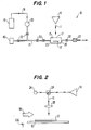
- FIG. 1 A method for removing surface contaminants from the surface of a substrate while preserving the molecular structure of the surface being treated is illustrated in Fig. 1.
- an assembly 10 holds a substrate 12 from which surface contaminants are to be removed.
- a gas 18 from gas source 16 is constantly flowed over substrate 12.
- Gas 18 is inert to substrate 12 and is flowed across substrate 12 so as to bathe substrate 12 in a non-reactive gas environment.
- gas 18 is a chemically inert gas such as helium, nitrogen or argon.
- An enclosure 15 for holding substrate 12 communicates with gas source 16 through a series of tubes 21, valves 22, and a gas flow meter 20.
- enclosure 15 comprises a stainless steel sample reaction cell fitted with opposing gas inlet and outlet ports 23, 25 respectively.
- Enclosure 15 is fitted with a sealed optical grade quartz window 17 through which irradiation can pass.
- Inlet and outlet ports 23, 25 may comprise, for example, stainless steel tubing fitted with valves.
- enclosure 15 is repeatedly flushed and backfilled with gas 18 and is kept at a pressure slightly above ambient atmospheric pressure to prevent inflow of other gases.
- enclosure 15 is shown as a solid chamber, it is anticipated that a surface being cleaned could be enclosed in any type of enclosure through which a gas can be flowed. For example, if the surface being treated is a large fixed object, a large portable enclosure such as a plastic bag might be utilized.
- Flow of gas 18 may be regulated by flow meter 20 which, in the preferred embodiment, is a Matheson Model 602 flow meter.
- Valves 22 are preferably metering, regulating or bellows valves suitable for high temperature and pressure applications and for use with toxic, hazardous, corrosive or expensive gases or liquids, as for example Swagelok SS-4HTM series valves by Swagelok Co. of Solon, Ohio. Valves 22 can be opened or closed to isolate enclosure 15, to communicate enclosure 15 with gas source 16 or to put enclosure 15 in communication with another substance, such as a gas for depositing on substrate 12, coming from an alternate source 40.
- the substrate treatment surface is irradiated with high-energy irradiation characterized by an energy density and duration between that required to release surface contaminants from the substrate treatment surface and that required to alter the molecular structure of the substrate treatment surface.
- a laser 14 generates laser irradiation which is directed against the treatment surface of substrate 12.
- laser 14 is shown as being outside enclosure 15 and irradiating sample 12 through quartz window 17. However, it is contemplated that laser 14 could alternatively be placed within the enclosure 15.
- the energy flux and the wavelength of the high-energy irradiation is preferably selected to be dependent upon the surface contaminants being removed.
- a gas analyzer 27 may be connected to outlet port 25. Analyzer 27 analyzes the contents of exhaust gas from enclosure 15 to facilitate selective energy and wavelength adjustment of laser 14.
- Gas analyzer 27 may be a mass spectrometer as for example a quadrapole mass spectrometer manufactured by Bruker Instruments, Inc. of Billerica, Massachusetts or by Perkin Elmer of Eden Prairie, Minnesota.
- the electron volt/photon (eV/photon) of the irradiation is preferably at least twice the energy necessary to break the bonds adhering the contaminants to the surface being cleaned.
- the bond energies between common contaminants such as carbon and oxygen, and common substrate materials such as silicon, titanium, germanium, iron, platinum and aluminum range between 2 and 7 eV/bond as disclosed in Handbook of Chemistry adn Physics, 68th ed., pp. F-169 to F-177 (CRC Press 1987). Accordingly, lasers emitting photons with energies in the range of 4 to 14 eV/photons are desirable.
- the wavelength should be below the wavelength that would compromise the integrity of the substrate surface by the photoelectric effect, as described in G.W. Castellan, Physical Chemistry , 2d ed., 458-459 (Academic Press, 1975).
- the preferred wavelength depends on the molecular species being removed and the resonance states of such species.
- the wavelengths and photon energies of a number of lasers operable in the invention are listed below. TABLE I Laser Wavelength (nm) eV/photon XeCl, pulsed 308 4.04 argon-ion, continuous wave 257 4.83 KrF, pulsed 248 5.01 ArF, pulsed 193 6.44 Tunable dye lasers, pulsed or continuous wave 200-800 1.55-6.22
- the irradiation directed against the substrate treatment surface has a power density less than that required to alter the molecular structure of the treatment surface from which contaminants are being removed.
- the power density of the irradiation and the duration of the irradiation are selected so as to impart an amount of energy on the substrate surface that is significantly below the energy required for alteration of the substrate surface structure.
- the preferred energy level is dependent on the composition of the substrate being treated. For example, with certain substrate materials such as plastics, this energy level would be much lower than for other materials such as high strength carbide steels. The heats of formation for various materials are well known and are reported in the Handbook of Chemistry and Physics , 68th ed., pp.
- the heat of formation generally corresponds to the amount of heat required to break down various materials and can be used as a guideline in selecting a laser irradiation energy level and duration that will not alter the molecular structure of the surface being treated.
- the heats of formation of a number of common substrate materials are summarized in the following table. TABLE II Material Heat of Formation A12O3 16906.7 kgJ/mol; 17.52 eV/molecule SiO2 840.3 kgJ/mol; 9.11 eV/molecule Nb2O5 1528.2 kgJ/mol; 13.27 eV/molecule NiO 230.6 kgJ/mol; 2.50 eV/molecule Ti2O3 500.2 kgJ/mol; 15.63 eV/molecule
- the irradiation energy density and duration of irradiation used in the present invention is such that the heat of formation is not approached on the substrate treatment surface. Finding the maximum energy usable on a given substrate material will require some experimentation in light of the material's known heat of formation. Thus, annealing, ablation and melting are prevented from occurring.
- a suitable trapping system may be connected to enclosure outlet 25 for trapping and neutralizing removed contaminant species.
- a substrate being treated may be selectively exposed to the laser irradiation by a variety of methods.
- substrate 12 is fixed on an XY table 13 which is selectively moved with respect to a fixed beam of laser pulses 11 that are directed through a beam splitter 24 and a focusing lens 28 before contacting selected portions of the surface of substrate 12 over which inert gas 18 flows.
- laser pulses 11 may be split by beam splitters 30, 32 into two sets of pulses which are selectively moved by adjusting mirrors 34-37 over the surface of substrate 12 on a fixed table 17.
- a laser power meter 26 allows for close monitoring of the laser power being applied to the substrate.
- the native oxide of silicon is necessary for the promotion of thin film growth on semiconductor sufaces.
- carbon contaminants adhere weakly to the semiconductor surface.
- the presence of these contaminants greatly reduces the conductivity or the insulating nature of the thin film to be deposited.
- Vacuum techniques are expensive especially if high or near ultra high vacuum is used to keep surfaces clean between processing steps.
- Chemical (wet & dry) and mechanical techniques can damage the substrate treatment surface and, if the substrate being treated is a processed integrated circuit, damage to the underlying structure may occur.
- a pulsed KrF excimer laser whose fundamental wavelength is 248 nm (UV range) was directed at the surface of a silicon substrate in a sealed box through which argon gas was flowed.
- argon gas was flowed.
- a precursor to aluminum thin film formation in semiconductor production irradiation of 35 mJ/cm2 for 6000 laser shots at a 10 Hz repetition rate was applied to a silicon oxide substrate surface with the KrF excimer laser.
- the laser treated surfaces were exposed during a continuous flow of argon gas at a flow rate of 16 1/hr under a 1.03 x 10³ torr backing regulator pressure. After treatment, XPS analysis showed the substrate exhibited a significant decrease in surface carbon from a pretreatment average surface carbon covering 30-45% of the substrate surface to an after treatment average surface carbon covering 19% of the substrate surface. The substrate surface itself showed no damage or alteration.
- a surface treated with laser irradiation as described above and then exposed to an organometallic gas flow showed, by XPS analysis, that 20.8% of the substrate surface was covered with carbon as compared to 40-45% of the substrate surface that was covered with carbon after organometallic gas exposure on a non-laser treated surface.
- the laser was applied, as described above, both prior to exposure to organometallic gas and again after gas exposure, only 8.9% of the surface was covered with carbon.
- Areas adjacent to the laser-exposed areas also exhibited some effects of the laser-cleaning treatment. Areas adjacent to the treated area showed a reduced carbon level of 12.7 percent. This effect probably is due to the gaussian nature of the applied laser pulse.
- Transfer of the wafer from the sample cell to the XPS analyzer was via an argon filled glove box.
- the silicon wafer was transferred to the XPS through an inert UHV transfer rod. This kept environmental exposure to a minimum.
- High energy optical components are difficult to fabricate for such technologies as laser fusion, x-ray lithography and UV excimer laser optics.
- Laser fusion and x-ray lithography technologies are used exclusively in "clean" environments.
- Excimer laser optics have a short work life span because with current commercial film deposition technology, it is difficult to fabricate films capable of withstanding prolonged high-energy fluxes.
- optical breakdown A perennial problem with high energy optics is optical breakdown. This phenomena can be described as "the catastrophic evolution of damage influcted in a transparent medium in a strong laser field.” Y.R. Shen, Principles of Nonlinear Optics , 1st ed., 528-540 (Wiley Interscience 1984). This phenomena occurs in solids as well as gases. With a solid, such as a high energy optic, optical breakdown is exacerbated by the presence of a surface defect such as scratches and pores in the bulk material. In most cases, optical breakdown is due to surface contamination such as adsorbed dust particles. The presence of these contaminants lowers the breakdown threshold which in turn limits the maximum laser power that can be used from a given laser system. This fact is a very important limitation regarding the pumping of a laser medium (solid state or gaseous) by an external pump Energy source. This, in turn, limits the laser power that can be used to transmit energy through optical windows, lenses and other optical components.
- Optical breakdown for example on a solid, is promoted by the presence of surface adhered contaminants.
- the interaction of a laser pulse train with a sufficient energy cross section may deposit enough energy to generate an "avalanche" ionization on the solid surface. This can form a surface plasma which may disintegrate the solid.
- the presence of contaminants effectively decreases the laser's efficiency and decreases its use in potential applications.
- the contaminant removal method can be used to remove adhered contaminants such as adsorbed dust.
- the component is exposed to a continuous flow of argon gas during which time a pulse KrF eximer laser is directed at the surface of the optical component.
- the laser is tuned to an appropriate energy flux and wavelength that is considerably less than the high energy pulse required to promote ionization and subsequent plasma in high energy optics.
- the optical component surface is irradiated at the selected flux and wavelength for a duration sufficent to remove adsorbed contaminants.
Landscapes
- Physics & Mathematics (AREA)
- Engineering & Computer Science (AREA)
- Optics & Photonics (AREA)
- Plasma & Fusion (AREA)
- Health & Medical Sciences (AREA)
- General Physics & Mathematics (AREA)
- Mechanical Engineering (AREA)
- Epidemiology (AREA)
- Public Health (AREA)
- Atmospheric Sciences (AREA)
- Environmental & Geological Engineering (AREA)
- Life Sciences & Earth Sciences (AREA)
- Toxicology (AREA)
- Cleaning Or Drying Semiconductors (AREA)
- Drying Of Semiconductors (AREA)
- Treatments Of Macromolecular Shaped Articles (AREA)
- Cleaning In General (AREA)
- Physical Or Chemical Processes And Apparatus (AREA)
- Electrodes Of Semiconductors (AREA)
- Paper (AREA)
- Electrical Discharge Machining, Electrochemical Machining, And Combined Machining (AREA)
- Calculators And Similar Devices (AREA)
Priority Applications (1)
| Application Number | Priority Date | Filing Date | Title |
|---|---|---|---|
| AT89112319T ATE88923T1 (de) | 1988-07-08 | 1989-07-06 | Entfernung von oberflaechen-verseuchungen durch ausstrahlung aus einer hoch-energiequelle. |
Applications Claiming Priority (2)
| Application Number | Priority Date | Filing Date | Title |
|---|---|---|---|
| US07/216,903 US5024968A (en) | 1988-07-08 | 1988-07-08 | Removal of surface contaminants by irradiation from a high-energy source |
| US216903 | 1988-07-08 |
Publications (3)
| Publication Number | Publication Date |
|---|---|
| EP0350021A2 true EP0350021A2 (de) | 1990-01-10 |
| EP0350021A3 EP0350021A3 (en) | 1990-05-23 |
| EP0350021B1 EP0350021B1 (de) | 1993-05-05 |
Family
ID=22808939
Family Applications (1)
| Application Number | Title | Priority Date | Filing Date |
|---|---|---|---|
| EP89112319A Expired - Lifetime EP0350021B1 (de) | 1988-07-08 | 1989-07-06 | Entfernung von Oberflächen-Verseuchungen durch Ausstrahlung aus einer Hoch-Energiequelle |
Country Status (16)
| Country | Link |
|---|---|
| US (1) | US5024968A (de) |
| EP (1) | EP0350021B1 (de) |
| JP (1) | JP2634245B2 (de) |
| KR (1) | KR0157608B1 (de) |
| AT (1) | ATE88923T1 (de) |
| AU (1) | AU620766B2 (de) |
| BR (1) | BR8907529A (de) |
| CA (1) | CA1328908C (de) |
| DE (1) | DE68906318T2 (de) |
| DK (1) | DK303490A (de) |
| ES (1) | ES2041374T3 (de) |
| FI (1) | FI910075A0 (de) |
| HK (1) | HK5195A (de) |
| LV (1) | LV11116B (de) |
| NO (1) | NO180739C (de) |
| WO (1) | WO1990000812A1 (de) |
Cited By (20)
| Publication number | Priority date | Publication date | Assignee | Title |
|---|---|---|---|---|
| WO1991011963A1 (fr) * | 1990-02-16 | 1991-08-22 | Universite De Nice-Sophia Antipolis | Sonde multicanalaire |
| FR2658412A1 (fr) * | 1990-02-19 | 1991-08-23 | Amiel Jean | Dispositif endoscopique notamment pour la destruction endoscopique de calcul par lithotritie. |
| GB2261548A (en) * | 1991-11-12 | 1993-05-19 | Motorola Inc | Crack resistant semiconductor package and method for making |
| EP0546178A4 (de) * | 1990-08-31 | 1994-02-23 | Takasago Netsugaku Kogyo Kabushiki Kaisha | |
| EP0597103A4 (en) * | 1991-07-25 | 1994-08-17 | Takasago Thermal Engineering | Apparatus for neutralizing charged body. |
| WO1994023854A1 (en) * | 1993-04-12 | 1994-10-27 | Cauldron Limited Partnership | Removal of surface contaminants by irradiation |
| WO1996041370A1 (en) * | 1995-06-07 | 1996-12-19 | Cauldron Limited Partnership | Removal of material by polarized radiation and back side application of radiation |
| US5756380A (en) * | 1995-11-02 | 1998-05-26 | Motorola, Inc. | Method for making a moisture resistant semiconductor device having an organic substrate |
| US5821175A (en) * | 1988-07-08 | 1998-10-13 | Cauldron Limited Partnership | Removal of surface contaminants by irradiation using various methods to achieve desired inert gas flow over treated surface |
| US6048588A (en) * | 1988-07-08 | 2000-04-11 | Cauldron Limited Partnership | Method for enhancing chemisorption of material |
| US6123803A (en) * | 1995-11-09 | 2000-09-26 | Oramir Semiconductor Equipment Ltd. | Laser processing chamber with cassette cell |
| US6350391B1 (en) | 1995-11-09 | 2002-02-26 | Oramir Semiconductor Equipment Ltd. | Laser stripping improvement by modified gas composition |
| SG97927A1 (en) * | 1999-09-02 | 2003-08-20 | Kubota Kk | Cleaning apparatus using a laser beam |
| GR20020100116A (el) * | 2002-03-01 | 2003-11-17 | Ιδρυμα Τεχνολογιας Και Ερευνας (Ι.Τ.Ε.) | Μεθοδος και συστημα για τον καθαρισμο επιφανειων με τη συγχρονη χρηση παλμων laser δυο διαφορετικων μηκων κυματος |
| EP1230989A3 (de) * | 2001-02-13 | 2004-03-10 | Canon Kabushiki Kaisha | Optisches Element zur Verwendung in einem Belichtungsapparat und Verfahren zur Spülung dieses optischen Elementes |
| FR2931009A1 (fr) * | 2008-05-07 | 2009-11-13 | Cnes Epic | Systeme ameliore de lecture optique d'informations memorisees sur un support reflechissant |
| US8389342B2 (en) | 2001-04-27 | 2013-03-05 | Semiconductor Energy Laboratory Co., Ltd. | Method for manufacturing a semiconductor device |
| CN104216240A (zh) * | 2014-09-17 | 2014-12-17 | 江苏影速光电技术有限公司 | 一种投影式曝光设备及使用方法 |
| WO2019134823A1 (de) * | 2018-01-03 | 2019-07-11 | Trumpf Laser- Und Systemtechnik Gmbh | Vorrichtung und verfahren zum abschwächen oder verstärken von laserinduzierter röntgenstrahlung |
| CN110883035A (zh) * | 2019-11-21 | 2020-03-17 | 中国核动力研究设计院 | 一种标准容器残余物料量的控制方法 |
Families Citing this family (120)
| Publication number | Priority date | Publication date | Assignee | Title |
|---|---|---|---|---|
| US5525727A (en) * | 1982-05-18 | 1996-06-11 | University Of Florida | Brain-specific drug delivery |
| US5643472A (en) * | 1988-07-08 | 1997-07-01 | Cauldron Limited Partnership | Selective removal of material by irradiation |
| US5531857A (en) * | 1988-07-08 | 1996-07-02 | Cauldron Limited Partnership | Removal of surface contaminants by irradiation from a high energy source |
| US5151135A (en) * | 1989-09-15 | 1992-09-29 | Amoco Corporation | Method for cleaning surfaces using UV lasers |
| JP2819166B2 (ja) * | 1989-10-03 | 1998-10-30 | キヤノン株式会社 | 放射光用光学素子の汚れ除去装置および方法 |
| US5493445A (en) * | 1990-03-29 | 1996-02-20 | The United States Of America As Represented By The Secretary Of The Navy | Laser textured surface absorber and emitter |
| US5322988A (en) * | 1990-03-29 | 1994-06-21 | The United States Of America As Represented By The Secretary Of The Navy | Laser texturing |
| US5093279A (en) * | 1991-02-01 | 1992-03-03 | International Business Machines Corporation | Laser ablation damascene process |
| US5695569A (en) * | 1991-02-28 | 1997-12-09 | Texas Instruments Incorporated | Removal of metal contamination |
| EP0502356A3 (en) * | 1991-02-28 | 1993-03-10 | Texas Instruments Incorporated | Photo-stimulated removal of trace metals |
| JP2920850B2 (ja) * | 1991-03-25 | 1999-07-19 | 東京エレクトロン株式会社 | 半導体の表面処理方法及びその装置 |
| US5571335A (en) * | 1991-12-12 | 1996-11-05 | Cold Jet, Inc. | Method for removal of surface coatings |
| US5194723A (en) * | 1991-12-24 | 1993-03-16 | Maxwell Laboratories, Inc. | Photoacoustic control of a pulsed light material removal process |
| US5328517A (en) * | 1991-12-24 | 1994-07-12 | Mcdonnell Douglas Corporation | Method and system for removing a coating from a substrate using radiant energy and a particle stream |
| US5204517A (en) * | 1991-12-24 | 1993-04-20 | Maxwell Laboratories, Inc. | Method and system for control of a material removal process using spectral emission discrimination |
| US5613509A (en) * | 1991-12-24 | 1997-03-25 | Maxwell Laboratories, Inc. | Method and apparatus for removing contaminants and coatings from a substrate using pulsed radiant energy and liquid carbon dioxide |
| US5281798A (en) * | 1991-12-24 | 1994-01-25 | Maxwell Laboratories, Inc. | Method and system for selective removal of material coating from a substrate using a flashlamp |
| US5782253A (en) * | 1991-12-24 | 1998-07-21 | Mcdonnell Douglas Corporation | System for removing a coating from a substrate |
| US5319183A (en) * | 1992-02-18 | 1994-06-07 | Fujitsu Limited | Method and apparatus for cutting patterns of printed wiring boards and method and apparatus for cleaning printed wiring boards |
| ATE180703T1 (de) * | 1992-03-31 | 1999-06-15 | Cauldron Lp | Entfernung von oberflächen-verseuchungen durch ausstrahlung |
| US5512123A (en) * | 1992-05-19 | 1996-04-30 | Maxwell Laboratories | Method for using pulsed optical energy to increase the bondability of a surface |
| TW372972B (en) * | 1992-10-23 | 1999-11-01 | Novartis Ag | Antiretroviral acyl compounds |
| US7037403B1 (en) | 1992-12-28 | 2006-05-02 | Applied Materials Inc. | In-situ real-time monitoring technique and apparatus for detection of thin films during chemical/mechanical polishing planarization |
| US6614529B1 (en) | 1992-12-28 | 2003-09-02 | Applied Materials, Inc. | In-situ real-time monitoring technique and apparatus for endpoint detection of thin films during chemical/mechanical polishing planarization |
| US6017397A (en) * | 1993-03-05 | 2000-01-25 | Hyundai Eletronics America | Automated washing method |
| US5373140A (en) * | 1993-03-16 | 1994-12-13 | Vernay Laboratories, Inc. | System for cleaning molding equipment using a laser |
| US5656096A (en) * | 1993-05-25 | 1997-08-12 | Polygon Industries, Inc. | Method for photopyrolitically removing a contaminant |
| US5482561A (en) * | 1993-06-11 | 1996-01-09 | Hughes Aircraft Company | Method for removing organic deposits from sand particles with laser beam |
| US5518956A (en) * | 1993-09-02 | 1996-05-21 | General Electric Company | Method of isolating vertical shorts in an electronic array using laser ablation |
| AU7682594A (en) * | 1993-09-08 | 1995-03-27 | Uvtech Systems, Inc. | Surface processing |
| US5814156A (en) * | 1993-09-08 | 1998-09-29 | Uvtech Systems Inc. | Photoreactive surface cleaning |
| JP3355251B2 (ja) * | 1993-11-02 | 2002-12-09 | 株式会社日立製作所 | 電子装置の製造方法 |
| GB9323052D0 (en) * | 1993-11-09 | 1994-01-05 | British Nuclear Fuels Plc | Radioactive decontamination |
| US5543356A (en) * | 1993-11-10 | 1996-08-06 | Hitachi, Ltd. | Method of impurity doping into semiconductor |
| US5584938A (en) * | 1993-12-10 | 1996-12-17 | Texas Instruments Incorporated | Electrostatic particle removal and characterization |
| GB9407058D0 (en) * | 1994-04-09 | 1994-06-01 | British Nuclear Fuels Plc | Material removal by laser ablation |
| US5516369A (en) * | 1994-05-06 | 1996-05-14 | United Microelectronics Corporation | Method and apparatus for particle reduction from semiconductor wafers |
| US5580421A (en) * | 1994-06-14 | 1996-12-03 | Fsi International | Apparatus for surface conditioning |
| US6015503A (en) * | 1994-06-14 | 2000-01-18 | Fsi International, Inc. | Method and apparatus for surface conditioning |
| GB9412238D0 (en) * | 1994-06-17 | 1994-08-10 | British Nuclear Fuels Plc | Removing contamination |
| WO1996006693A1 (en) * | 1994-08-29 | 1996-03-07 | Uvtech Systems, Inc. | Photo reactive cleaning of critical surfaces in cd manufacturing |
| AU3460895A (en) * | 1994-08-29 | 1996-03-22 | Uvtech Systems, Inc. | Surface modification processing of flat panel device substrates |
| WO1996006692A1 (en) * | 1994-08-29 | 1996-03-07 | Uvtech Systems, Inc. | Cleaning of printed circuit boards |
| US6537133B1 (en) | 1995-03-28 | 2003-03-25 | Applied Materials, Inc. | Method for in-situ endpoint detection for chemical mechanical polishing operations |
| US5964643A (en) * | 1995-03-28 | 1999-10-12 | Applied Materials, Inc. | Apparatus and method for in-situ monitoring of chemical mechanical polishing operations |
| US6876454B1 (en) | 1995-03-28 | 2005-04-05 | Applied Materials, Inc. | Apparatus and method for in-situ endpoint detection for chemical mechanical polishing operations |
| US5637245A (en) * | 1995-04-13 | 1997-06-10 | Vernay Laboratories, Inc. | Method and apparatus for minimizing degradation of equipment in a laser cleaning technique |
| US6027960A (en) | 1995-10-25 | 2000-02-22 | Semiconductor Energy Laboratory Co., Ltd. | Laser annealing method and laser annealing device |
| IL115933A0 (en) | 1995-11-09 | 1996-01-31 | Oramir Semiconductor Ltd | Process and apparatus for oblique beam revolution for the effective laser stripping of sidewalls |
| US5998305A (en) * | 1996-03-29 | 1999-12-07 | Praxair Technology, Inc. | Removal of carbon from substrate surfaces |
| US5800625A (en) * | 1996-07-26 | 1998-09-01 | Cauldron Limited Partnership | Removal of material by radiation applied at an oblique angle |
| US8066819B2 (en) | 1996-12-19 | 2011-11-29 | Best Label Co., Inc. | Method of removing organic materials from substrates |
| US6146541A (en) * | 1997-05-02 | 2000-11-14 | Motorola, Inc. | Method of manufacturing a semiconductor device that uses a calibration standard |
| US6066032A (en) * | 1997-05-02 | 2000-05-23 | Eco Snow Systems, Inc. | Wafer cleaning using a laser and carbon dioxide snow |
| JPH11102867A (ja) | 1997-07-16 | 1999-04-13 | Sony Corp | 半導体薄膜の形成方法およびプラスチック基板 |
| US5954974A (en) * | 1997-09-25 | 1999-09-21 | Lucent Technologies Inc. | Laser-assisted coating removal from optical fibers |
| US6165273A (en) | 1997-10-21 | 2000-12-26 | Fsi International Inc. | Equipment for UV wafer heating and photochemistry |
| US6301080B1 (en) | 1998-02-17 | 2001-10-09 | Seagate Technology Llc | Dither method to unload negative suction air bearings |
| US6494217B2 (en) | 1998-03-12 | 2002-12-17 | Motorola, Inc. | Laser cleaning process for semiconductor material and the like |
| US6394105B1 (en) * | 1998-03-19 | 2002-05-28 | Seagate Technology, Inc. | Integrated laser cleaning and inspection system for rigid thin film media for magnetic recording application |
| US20010050091A1 (en) * | 1998-03-19 | 2001-12-13 | Seagate Technology Llc | Method apparatus of disc burnishing with a glide/burnish head |
| US6113708A (en) * | 1998-05-26 | 2000-09-05 | Candescent Technologies Corporation | Cleaning of flat-panel display |
| DE19830438A1 (de) | 1998-07-08 | 2000-01-13 | Zeiss Carl Fa | Verfahren zur Dekontamination von Mikrolithographie-Projektionsbelichtungsanlagen |
| US6178973B1 (en) | 1998-07-28 | 2001-01-30 | International Business Machines Corporation | Method and apparatus for ozone generation and surface treatment |
| JP2000133736A (ja) * | 1998-10-26 | 2000-05-12 | Furukawa Electric Co Ltd:The | 半導体レーザ素子の気密封止方法及び気密封止装置 |
| US6099762A (en) * | 1998-12-21 | 2000-08-08 | Lewis; Paul E. | Method for improving lubricating surfaces on disks |
| IL127720A0 (en) | 1998-12-24 | 1999-10-28 | Oramir Semiconductor Ltd | Local particle cleaning |
| US6217422B1 (en) * | 1999-01-20 | 2001-04-17 | International Business Machines Corporation | Light energy cleaning of polishing pads |
| US6994607B2 (en) | 2001-12-28 | 2006-02-07 | Applied Materials, Inc. | Polishing pad with window |
| JP2002542043A (ja) * | 1999-04-27 | 2002-12-10 | ジーエスアイ ルモニクス インコーポレイテッド | 多重レーザビームを使用する材料処理システム及び方法 |
| US6881687B1 (en) | 1999-10-29 | 2005-04-19 | Paul P. Castrucci | Method for laser cleaning of a substrate surface using a solid sacrificial film |
| JP2001144003A (ja) | 1999-11-16 | 2001-05-25 | Canon Inc | 露光装置およびデバイス製造方法 |
| DE19957034B4 (de) * | 1999-11-26 | 2006-04-13 | Heraeus Noblelight Gmbh | Verfahren zur Behandlung von Oberflächen von Substraten und Vorrichtung |
| US6861364B1 (en) * | 1999-11-30 | 2005-03-01 | Canon Kabushiki Kaisha | Laser etching method and apparatus therefor |
| US6627846B1 (en) | 1999-12-16 | 2003-09-30 | Oramir Semiconductor Equipment Ltd. | Laser-driven cleaning using reactive gases |
| US6582857B1 (en) | 2000-03-16 | 2003-06-24 | International Business Machines Corporation | Repair of masks to promote adhesion of patches |
| US6500268B1 (en) | 2000-08-18 | 2002-12-31 | Silicon Genesis Corporation | Dry cleaning method |
| US6526997B1 (en) | 2000-08-18 | 2003-03-04 | Francois J. Henley | Dry cleaning method for the manufacture of integrated circuits |
| US6726549B2 (en) * | 2000-09-08 | 2004-04-27 | Cold Jet, Inc. | Particle blast apparatus |
| DE10061248B4 (de) * | 2000-12-09 | 2004-02-26 | Carl Zeiss | Verfahren und Vorrichtung zur In-situ-Dekontamination eines EUV-Lithographiegerätes |
| US6512198B2 (en) | 2001-05-15 | 2003-01-28 | Lexmark International, Inc | Removal of debris from laser ablated nozzle plates |
| US7087504B2 (en) * | 2001-05-18 | 2006-08-08 | Semiconductor Energy Laboratory Co., Ltd. | Method of manufacturing a semiconductor device by irradiating with a laser beam |
| US6799584B2 (en) * | 2001-11-09 | 2004-10-05 | Applied Materials, Inc. | Condensation-based enhancement of particle removal by suction |
| WO2003066245A1 (en) * | 2002-02-01 | 2003-08-14 | Metastable Instruments, Inc. | Method and apparatus for cleaning with electromagnetic radiation |
| DE10208718A1 (de) * | 2002-02-28 | 2003-10-02 | Wacker Siltronic Halbleitermat | Verfahren zur Entfernung von Partikeln von Oberflächen |
| JP4117293B2 (ja) * | 2002-06-14 | 2008-07-16 | コーニンクレッカ フィリップス エレクトロニクス エヌ ヴィ | 情報担体を走査及びクリーニングする装置 |
| AU2003251606A1 (en) * | 2002-07-25 | 2004-02-16 | Arkansas State University | Method and apparatus for removing minute particle(s) from a surface |
| US6908567B2 (en) * | 2002-07-30 | 2005-06-21 | Applied Materials Israel, Ltd. | Contaminant removal by laser-accelerated fluid |
| US6829035B2 (en) * | 2002-11-12 | 2004-12-07 | Applied Materials Israel, Ltd. | Advanced mask cleaning and handling |
| US6747243B1 (en) | 2002-12-24 | 2004-06-08 | Novellus Systems, Inc. | Spot cleaning of particles after inspection |
| US6838395B1 (en) * | 2002-12-30 | 2005-01-04 | Matsushita Electric Industrial Co., Ltd. | Method for fabricating a semiconductor crystal |
| US6864458B2 (en) * | 2003-01-21 | 2005-03-08 | Applied Materials, Inc. | Iced film substrate cleaning |
| US20040224508A1 (en) * | 2003-05-06 | 2004-11-11 | Applied Materials Israel Ltd | Apparatus and method for cleaning a substrate using a homogenized and non-polarized radiation beam |
| WO2005038877A2 (en) * | 2003-10-14 | 2005-04-28 | Rudolph Technologies, Inc. | MOLECULAR AIRBORNE CONTAMINANTS (MACs) REMOVAL AND WAFER SURFACE SUSTAINING SYSTEM AND METHOD |
| US7303636B1 (en) * | 2003-10-16 | 2007-12-04 | Hutchinson Technology Incorporated | Method of laser cleaning surfaces on a head suspension |
| US20050082348A1 (en) * | 2003-10-17 | 2005-04-21 | Maier Robert L. | Method for bonding glass or metal fluoride optical materials to metal |
| US20050279453A1 (en) * | 2004-06-17 | 2005-12-22 | Uvtech Systems, Inc. | System and methods for surface cleaning |
| KR20060020045A (ko) * | 2004-08-30 | 2006-03-06 | 삼성에스디아이 주식회사 | 유기전계발광표시장치의 제조방법 |
| RU2297886C2 (ru) * | 2005-06-06 | 2007-04-27 | Евгений Михайлович Борисов | Способ очистки поверхности и устройство для его осуществления |
| JP2007027419A (ja) * | 2005-07-15 | 2007-02-01 | Canon Inc | 露光装置 |
| CN100437279C (zh) * | 2005-08-15 | 2008-11-26 | 友达光电股份有限公司 | 有源光罩除尘设备 |
| JP4772610B2 (ja) * | 2006-07-19 | 2011-09-14 | 東京エレクトロン株式会社 | 分析方法 |
| JP2008147314A (ja) * | 2006-12-07 | 2008-06-26 | Canon Inc | 洗浄装置及び方法、洗浄装置を有する露光装置 |
| JP2008193035A (ja) * | 2007-02-08 | 2008-08-21 | Matsushita Electric Ind Co Ltd | 微細形状転写方法および微細形状転写装置 |
| US20080296258A1 (en) * | 2007-02-08 | 2008-12-04 | Elliott David J | Plenum reactor system |
| US11311917B2 (en) | 2007-08-09 | 2022-04-26 | Bruker Nano, Inc. | Apparatus and method for contamination identification |
| JP2009302136A (ja) * | 2008-06-10 | 2009-12-24 | Panasonic Corp | 半導体集積回路 |
| JP2011527637A (ja) * | 2008-07-09 | 2011-11-04 | エフ・イ−・アイ・カンパニー | レーザ機械加工のための方法および装置 |
| US8801497B2 (en) | 2009-04-30 | 2014-08-12 | Rdc Holdings, Llc | Array of abrasive members with resilient support |
| US9221148B2 (en) | 2009-04-30 | 2015-12-29 | Rdc Holdings, Llc | Method and apparatus for processing sliders for disk drives, and to various processing media for the same |
| US20110104989A1 (en) * | 2009-04-30 | 2011-05-05 | First Principles LLC | Dressing bar for embedding abrasive particles into substrates |
| US20100330890A1 (en) | 2009-06-30 | 2010-12-30 | Zine-Eddine Boutaghou | Polishing pad with array of fluidized gimballed abrasive members |
| US9017933B2 (en) * | 2010-03-29 | 2015-04-28 | Tokyo Electron Limited | Method for integrating low-k dielectrics |
| US10907305B2 (en) | 2013-02-21 | 2021-02-02 | REEP Technologies Ltd. | System and method for reprinting on paper |
| CN105143551B (zh) * | 2013-02-21 | 2017-11-03 | Reep技术有限公司 | 一种用于纸质打印的系统和方法 |
| JP6382901B2 (ja) | 2016-09-29 | 2018-08-29 | ファナック株式会社 | レーザー加工システム |
| KR102500603B1 (ko) * | 2017-01-06 | 2023-02-17 | 레이브 엘엘씨 | 오염 식별 장치 및 방법 |
| US10610963B2 (en) * | 2017-05-17 | 2020-04-07 | General Electric Company | Surface treatment of turbomachinery |
| DE102019101095A1 (de) * | 2019-01-16 | 2020-07-16 | RWE Nuclear GmbH | Verfahren und Vorrichtung zum Aufbereiten eines kontaminierten Werkstücks |
| US11440062B2 (en) * | 2019-11-07 | 2022-09-13 | General Electric Company | System and method for cleaning a tube |
Citations (4)
| Publication number | Priority date | Publication date | Assignee | Title |
|---|---|---|---|---|
| US3464534A (en) | 1966-03-21 | 1969-09-02 | Hrand M Muncheryan | Laser eraser |
| US4181538A (en) | 1978-09-26 | 1980-01-01 | The United States Of America As Represented By The United States Department Of Energy | Method for making defect-free zone by laser-annealing of doped silicon |
| US4292093A (en) | 1979-12-28 | 1981-09-29 | The United States Of America As Represented By The United States Department Of Energy | Method using laser irradiation for the production of atomically clean crystalline silicon and germanium surfaces |
| US4680616A (en) | 1986-05-09 | 1987-07-14 | Chronar Corp. | Removal of defects from semiconductors |
Family Cites Families (15)
| Publication number | Priority date | Publication date | Assignee | Title |
|---|---|---|---|---|
| US3364087A (en) * | 1964-04-27 | 1968-01-16 | Varian Associates | Method of using laser to coat or etch substrate |
| US3503804A (en) * | 1967-04-25 | 1970-03-31 | Hellmut Schneider | Method and apparatus for the production of sonic or ultrasonic waves on a surface |
| JPS567439A (en) * | 1979-06-29 | 1981-01-26 | Sony Corp | Treating method for semiconductor substrate |
| US4305973A (en) * | 1979-07-24 | 1981-12-15 | Hughes Aircraft Company | Laser annealed double conductor structure |
| JPS588128B2 (ja) * | 1979-08-05 | 1983-02-14 | 山崎 舜平 | 半導体装置作製方法 |
| JPS5776846A (en) * | 1980-10-31 | 1982-05-14 | Fujitsu Ltd | Surface treating method for semiconductor |
| JPS57102229A (en) * | 1980-12-17 | 1982-06-25 | Matsushita Electric Ind Co Ltd | Substrate processing method |
| JPS57187936A (en) * | 1981-05-14 | 1982-11-18 | Nec Corp | Manufacture of 3-5 family compound semiconductor element |
| JPS59215728A (ja) * | 1983-05-24 | 1984-12-05 | Semiconductor Energy Lab Co Ltd | 半導体表面の光洗浄方法 |
| JPS6037736A (ja) * | 1983-08-11 | 1985-02-27 | Toshiba Corp | 表面清浄方法 |
| US4668304A (en) * | 1985-04-10 | 1987-05-26 | Eaton Corporation | Dopant gettering semiconductor processing by excimer laser |
| JPS6286709A (ja) * | 1985-10-11 | 1987-04-21 | Mitsubishi Electric Corp | 半導体装置の製造方法 |
| EP0251280A3 (de) * | 1986-06-30 | 1989-11-23 | Nec Corporation | Laserverfahren zur Getterung für Halbleiterscheiben |
| DE3824048A1 (de) * | 1988-07-15 | 1990-05-03 | Fraunhofer Ges Forschung | Verfahren und vorrichtung zum bearbeiten von werkstuecken mit laserstrahlung |
| JPH0637736A (ja) * | 1992-07-16 | 1994-02-10 | Matsushita Electric Ind Co Ltd | 同期保持装置 |
-
1988
- 1988-07-08 US US07/216,903 patent/US5024968A/en not_active Expired - Lifetime
-
1989
- 1989-07-06 ES ES198989112319T patent/ES2041374T3/es not_active Expired - Lifetime
- 1989-07-06 AT AT89112319T patent/ATE88923T1/de not_active IP Right Cessation
- 1989-07-06 DE DE89112319T patent/DE68906318T2/de not_active Expired - Fee Related
- 1989-07-06 EP EP89112319A patent/EP0350021B1/de not_active Expired - Lifetime
- 1989-07-07 BR BR898907529A patent/BR8907529A/pt not_active Application Discontinuation
- 1989-07-07 CA CA000605060A patent/CA1328908C/en not_active Expired - Fee Related
- 1989-07-07 FI FI910075A patent/FI910075A0/fi unknown
- 1989-07-07 KR KR1019890009662A patent/KR0157608B1/ko not_active Expired - Fee Related
- 1989-07-07 AU AU38676/89A patent/AU620766B2/en not_active Ceased
- 1989-07-07 WO PCT/US1989/002952 patent/WO1990000812A1/en not_active Ceased
- 1989-07-10 JP JP1177848A patent/JP2634245B2/ja not_active Expired - Fee Related
-
1990
- 1990-12-21 DK DK303490A patent/DK303490A/da not_active Application Discontinuation
-
1991
- 1991-01-07 NO NO910067A patent/NO180739C/no not_active IP Right Cessation
-
1994
- 1994-05-04 LV LVP-94-95A patent/LV11116B/en unknown
-
1995
- 1995-01-12 HK HK5195A patent/HK5195A/en not_active IP Right Cessation
Patent Citations (4)
| Publication number | Priority date | Publication date | Assignee | Title |
|---|---|---|---|---|
| US3464534A (en) | 1966-03-21 | 1969-09-02 | Hrand M Muncheryan | Laser eraser |
| US4181538A (en) | 1978-09-26 | 1980-01-01 | The United States Of America As Represented By The United States Department Of Energy | Method for making defect-free zone by laser-annealing of doped silicon |
| US4292093A (en) | 1979-12-28 | 1981-09-29 | The United States Of America As Represented By The United States Department Of Energy | Method using laser irradiation for the production of atomically clean crystalline silicon and germanium surfaces |
| US4680616A (en) | 1986-05-09 | 1987-07-14 | Chronar Corp. | Removal of defects from semiconductors |
Non-Patent Citations (5)
| Title |
|---|
| "CRC Handbook of Laser Science", vol. 1-5, 1982 |
| "Handbook of Chemistry adn Physics", 1987, CRC PRESS, pages: F-169 - F-177 |
| "Handbook of Chemistry and Physics", 1987, CRC PRESS, pages: D33 - D42 |
| G.W. CASTELLAN: "Physical Chemistry", 1975, ACADEMIC PRESS, pages: 458 - 459 |
| MITSUO MAEDA: "Laser Dyes", 1984, ACADEMIC PRESS |
Cited By (28)
| Publication number | Priority date | Publication date | Assignee | Title |
|---|---|---|---|---|
| US6048588A (en) * | 1988-07-08 | 2000-04-11 | Cauldron Limited Partnership | Method for enhancing chemisorption of material |
| US5821175A (en) * | 1988-07-08 | 1998-10-13 | Cauldron Limited Partnership | Removal of surface contaminants by irradiation using various methods to achieve desired inert gas flow over treated surface |
| US5342350A (en) * | 1990-02-16 | 1994-08-30 | Jean Amiel | Method of endoscopically treating lithiases with a multichannel probe suitable for draining the treated lithiases |
| WO1991011963A1 (fr) * | 1990-02-16 | 1991-08-22 | Universite De Nice-Sophia Antipolis | Sonde multicanalaire |
| FR2658412A1 (fr) * | 1990-02-19 | 1991-08-23 | Amiel Jean | Dispositif endoscopique notamment pour la destruction endoscopique de calcul par lithotritie. |
| EP0546178A4 (de) * | 1990-08-31 | 1994-02-23 | Takasago Netsugaku Kogyo Kabushiki Kaisha | |
| EP0597103A4 (en) * | 1991-07-25 | 1994-08-17 | Takasago Thermal Engineering | Apparatus for neutralizing charged body. |
| GB2261548A (en) * | 1991-11-12 | 1993-05-19 | Motorola Inc | Crack resistant semiconductor package and method for making |
| WO1994023854A1 (en) * | 1993-04-12 | 1994-10-27 | Cauldron Limited Partnership | Removal of surface contaminants by irradiation |
| AU684772B2 (en) * | 1993-04-12 | 1998-01-08 | Cauldron Limited Partnership | Removal of surface contaminants by irradiation |
| CN1066644C (zh) * | 1993-04-12 | 2001-06-06 | 大锅有限合伙人公司 | 表面沾污物的清除方法和设备 |
| WO1996041370A1 (en) * | 1995-06-07 | 1996-12-19 | Cauldron Limited Partnership | Removal of material by polarized radiation and back side application of radiation |
| CN100390938C (zh) * | 1995-06-07 | 2008-05-28 | 大锅有限合伙人公司 | 用偏振辐照和背面辐照清除物质的方法 |
| US5958268A (en) * | 1995-06-07 | 1999-09-28 | Cauldron Limited Partnership | Removal of material by polarized radiation |
| US5756380A (en) * | 1995-11-02 | 1998-05-26 | Motorola, Inc. | Method for making a moisture resistant semiconductor device having an organic substrate |
| US6123803A (en) * | 1995-11-09 | 2000-09-26 | Oramir Semiconductor Equipment Ltd. | Laser processing chamber with cassette cell |
| US6350391B1 (en) | 1995-11-09 | 2002-02-26 | Oramir Semiconductor Equipment Ltd. | Laser stripping improvement by modified gas composition |
| SG97927A1 (en) * | 1999-09-02 | 2003-08-20 | Kubota Kk | Cleaning apparatus using a laser beam |
| EP1230989A3 (de) * | 2001-02-13 | 2004-03-10 | Canon Kabushiki Kaisha | Optisches Element zur Verwendung in einem Belichtungsapparat und Verfahren zur Spülung dieses optischen Elementes |
| US8389342B2 (en) | 2001-04-27 | 2013-03-05 | Semiconductor Energy Laboratory Co., Ltd. | Method for manufacturing a semiconductor device |
| EP1340556A3 (de) * | 2002-03-01 | 2003-12-17 | Foundation for Research and Technology-Hellas (FO.R.T.H.), Institute of Electronic Structure and Laser | Verfahren und Vorrichtung zum Reinigen von Flächen mit zeitweise gleichzeitigen Laserimpulsen zweier unterschiedlicher Wellenlängen |
| GR20020100116A (el) * | 2002-03-01 | 2003-11-17 | Ιδρυμα Τεχνολογιας Και Ερευνας (Ι.Τ.Ε.) | Μεθοδος και συστημα για τον καθαρισμο επιφανειων με τη συγχρονη χρηση παλμων laser δυο διαφορετικων μηκων κυματος |
| FR2931009A1 (fr) * | 2008-05-07 | 2009-11-13 | Cnes Epic | Systeme ameliore de lecture optique d'informations memorisees sur un support reflechissant |
| WO2009141552A3 (fr) * | 2008-05-07 | 2010-02-18 | Centre National D'etudes Spatiales | Systeme ameliore de lecture optique d'informations memorisees sur un support reflechissant |
| CN104216240A (zh) * | 2014-09-17 | 2014-12-17 | 江苏影速光电技术有限公司 | 一种投影式曝光设备及使用方法 |
| WO2019134823A1 (de) * | 2018-01-03 | 2019-07-11 | Trumpf Laser- Und Systemtechnik Gmbh | Vorrichtung und verfahren zum abschwächen oder verstärken von laserinduzierter röntgenstrahlung |
| CN110883035A (zh) * | 2019-11-21 | 2020-03-17 | 中国核动力研究设计院 | 一种标准容器残余物料量的控制方法 |
| CN110883035B (zh) * | 2019-11-21 | 2021-05-04 | 中国核动力研究设计院 | 一种标准容器残余物料量的控制方法 |
Also Published As
| Publication number | Publication date |
|---|---|
| WO1990000812A1 (en) | 1990-01-25 |
| US5024968A (en) | 1991-06-18 |
| JP2634245B2 (ja) | 1997-07-23 |
| JPH0286128A (ja) | 1990-03-27 |
| BR8907529A (pt) | 1991-06-11 |
| EP0350021A3 (en) | 1990-05-23 |
| NO180739B (no) | 1997-02-24 |
| DE68906318T2 (de) | 1993-10-07 |
| FI910075A7 (fi) | 1991-01-07 |
| AU620766B2 (en) | 1992-02-20 |
| LV11116B (en) | 1996-10-20 |
| DK303490D0 (da) | 1990-12-21 |
| HK5195A (en) | 1995-01-20 |
| DK303490A (da) | 1991-02-25 |
| FI910075A0 (fi) | 1991-01-07 |
| EP0350021B1 (de) | 1993-05-05 |
| CA1328908C (en) | 1994-04-26 |
| NO910067L (no) | 1991-01-07 |
| KR900002414A (ko) | 1990-02-28 |
| DE68906318D1 (de) | 1993-06-09 |
| ATE88923T1 (de) | 1993-05-15 |
| ES2041374T3 (es) | 1993-11-16 |
| KR0157608B1 (ko) | 1998-12-01 |
| LV11116A (lv) | 1996-04-20 |
| AU3867689A (en) | 1990-02-05 |
| NO910067D0 (no) | 1991-01-07 |
| NO180739C (no) | 1997-06-04 |
Similar Documents
| Publication | Publication Date | Title |
|---|---|---|
| EP0350021B1 (de) | Entfernung von Oberflächen-Verseuchungen durch Ausstrahlung aus einer Hoch-Energiequelle | |
| US5099557A (en) | Removal of surface contaminants by irradiation from a high-energy source | |
| US5531857A (en) | Removal of surface contaminants by irradiation from a high energy source | |
| US5821175A (en) | Removal of surface contaminants by irradiation using various methods to achieve desired inert gas flow over treated surface | |
| EP0693978B1 (de) | Entfernung von oberflächen-verschmutzungen durch bestrahlung | |
| US5800625A (en) | Removal of material by radiation applied at an oblique angle | |
| EP0782483B1 (de) | Selektive entfernung von material durch bestrahlung | |
| US5151135A (en) | Method for cleaning surfaces using UV lasers | |
| EP0633823B1 (de) | Entfernung von oberflächen-verseuchungen durch ausstrahlung | |
| US6881687B1 (en) | Method for laser cleaning of a substrate surface using a solid sacrificial film | |
| WO1998054632A2 (en) | Semiconductor wafer processing with defect eradication | |
| RU2099811C1 (ru) | Способ удаления поверхностных примесей с поверхности подложки и устройство для его осуществления | |
| Engelsberg | Particle Removal from Semiconductor Surfaces Using a Photon-Assisted, Gas-Phase Cleaning Process | |
| CA2259910C (en) | Removal of material by radiation applied at an oblique angle |
Legal Events
| Date | Code | Title | Description |
|---|---|---|---|
| PUAI | Public reference made under article 153(3) epc to a published international application that has entered the european phase |
Free format text: ORIGINAL CODE: 0009012 |
|
| AK | Designated contracting states |
Kind code of ref document: A2 Designated state(s): AT BE CH DE ES FR GB GR IT LI LU NL SE |
|
| PUAL | Search report despatched |
Free format text: ORIGINAL CODE: 0009013 |
|
| RHK1 | Main classification (correction) |
Ipc: B08B 7/00 |
|
| AK | Designated contracting states |
Kind code of ref document: A3 Designated state(s): AT BE CH DE ES FR GB GR IT LI LU NL SE |
|
| 17P | Request for examination filed |
Effective date: 19901109 |
|
| 17Q | First examination report despatched |
Effective date: 19910912 |
|
| GRAA | (expected) grant |
Free format text: ORIGINAL CODE: 0009210 |
|
| RAP1 | Party data changed (applicant data changed or rights of an application transferred) |
Owner name: CAULDRON LIMITED PARTNERSHIP |
|
| AK | Designated contracting states |
Kind code of ref document: B1 Designated state(s): AT BE CH DE ES FR GB GR IT LI LU NL SE |
|
| REF | Corresponds to: |
Ref document number: 88923 Country of ref document: AT Date of ref document: 19930515 Kind code of ref document: T |
|
| ITF | It: translation for a ep patent filed | ||
| REF | Corresponds to: |
Ref document number: 68906318 Country of ref document: DE Date of ref document: 19930609 |
|
| ET | Fr: translation filed | ||
| REG | Reference to a national code |
Ref country code: GR Ref legal event code: FG4A Free format text: 3008370 |
|
| REG | Reference to a national code |
Ref country code: ES Ref legal event code: FG2A Ref document number: 2041374 Country of ref document: ES Kind code of ref document: T3 |
|
| PLBE | No opposition filed within time limit |
Free format text: ORIGINAL CODE: 0009261 |
|
| STAA | Information on the status of an ep patent application or granted ep patent |
Free format text: STATUS: NO OPPOSITION FILED WITHIN TIME LIMIT |
|
| 26N | No opposition filed | ||
| ITTA | It: last paid annual fee | ||
| EPTA | Lu: last paid annual fee | ||
| EAL | Se: european patent in force in sweden |
Ref document number: 89112319.2 |
|
| PGFP | Annual fee paid to national office [announced via postgrant information from national office to epo] |
Ref country code: AT Payment date: 19980707 Year of fee payment: 10 |
|
| PGFP | Annual fee paid to national office [announced via postgrant information from national office to epo] |
Ref country code: SE Payment date: 19980709 Year of fee payment: 10 |
|
| PGFP | Annual fee paid to national office [announced via postgrant information from national office to epo] |
Ref country code: ES Payment date: 19980716 Year of fee payment: 10 |
|
| PGFP | Annual fee paid to national office [announced via postgrant information from national office to epo] |
Ref country code: GR Payment date: 19980722 Year of fee payment: 10 |
|
| PGFP | Annual fee paid to national office [announced via postgrant information from national office to epo] |
Ref country code: LU Payment date: 19980826 Year of fee payment: 10 |
|
| PG25 | Lapsed in a contracting state [announced via postgrant information from national office to epo] |
Ref country code: LU Free format text: LAPSE BECAUSE OF NON-PAYMENT OF DUE FEES Effective date: 19990706 Ref country code: AT Free format text: LAPSE BECAUSE OF NON-PAYMENT OF DUE FEES Effective date: 19990706 |
|
| PG25 | Lapsed in a contracting state [announced via postgrant information from national office to epo] |
Ref country code: ES Free format text: LAPSE BECAUSE OF NON-PAYMENT OF DUE FEES Effective date: 19990707 |
|
| PGFP | Annual fee paid to national office [announced via postgrant information from national office to epo] |
Ref country code: CH Payment date: 19990728 Year of fee payment: 11 |
|
| PG25 | Lapsed in a contracting state [announced via postgrant information from national office to epo] |
Ref country code: SE Free format text: THE PATENT HAS BEEN ANNULLED BY A DECISION OF A NATIONAL AUTHORITY Effective date: 19990730 |
|
| PG25 | Lapsed in a contracting state [announced via postgrant information from national office to epo] |
Ref country code: GR Free format text: LAPSE BECAUSE OF NON-PAYMENT OF DUE FEES Effective date: 19990731 |
|
| PGFP | Annual fee paid to national office [announced via postgrant information from national office to epo] |
Ref country code: BE Payment date: 19990809 Year of fee payment: 11 |
|
| EUG | Se: european patent has lapsed |
Ref document number: 89112319.2 |
|
| PG25 | Lapsed in a contracting state [announced via postgrant information from national office to epo] |
Ref country code: LI Free format text: LAPSE BECAUSE OF NON-PAYMENT OF DUE FEES Effective date: 20000731 Ref country code: BE Free format text: LAPSE BECAUSE OF NON-PAYMENT OF DUE FEES Effective date: 20000731 Ref country code: CH Free format text: LAPSE BECAUSE OF NON-PAYMENT OF DUE FEES Effective date: 20000731 |
|
| BERE | Be: lapsed |
Owner name: CAULDRON LTD PARTNERSHIP Effective date: 20000731 |
|
| REG | Reference to a national code |
Ref country code: CH Ref legal event code: PL |
|
| REG | Reference to a national code |
Ref country code: GB Ref legal event code: IF02 |
|
| REG | Reference to a national code |
Ref country code: ES Ref legal event code: FD2A Effective date: 20000810 |
|
| PGFP | Annual fee paid to national office [announced via postgrant information from national office to epo] |
Ref country code: IT Payment date: 20060731 Year of fee payment: 18 |
|
| PGFP | Annual fee paid to national office [announced via postgrant information from national office to epo] |
Ref country code: GB Payment date: 20070711 Year of fee payment: 19 |
|
| PGFP | Annual fee paid to national office [announced via postgrant information from national office to epo] |
Ref country code: NL Payment date: 20070723 Year of fee payment: 19 |
|
| PGFP | Annual fee paid to national office [announced via postgrant information from national office to epo] |
Ref country code: FR Payment date: 20070725 Year of fee payment: 19 |
|
| PGFP | Annual fee paid to national office [announced via postgrant information from national office to epo] |
Ref country code: DE Payment date: 20071231 Year of fee payment: 19 |
|
| GBPC | Gb: european patent ceased through non-payment of renewal fee |
Effective date: 20080706 |
|
| NLV4 | Nl: lapsed or anulled due to non-payment of the annual fee |
Effective date: 20090201 |
|
| PG25 | Lapsed in a contracting state [announced via postgrant information from national office to epo] |
Ref country code: DE Free format text: LAPSE BECAUSE OF NON-PAYMENT OF DUE FEES Effective date: 20090203 |
|
| REG | Reference to a national code |
Ref country code: FR Ref legal event code: ST Effective date: 20090331 |
|
| PG25 | Lapsed in a contracting state [announced via postgrant information from national office to epo] |
Ref country code: NL Free format text: LAPSE BECAUSE OF NON-PAYMENT OF DUE FEES Effective date: 20090201 |
|
| PG25 | Lapsed in a contracting state [announced via postgrant information from national office to epo] |
Ref country code: GB Free format text: LAPSE BECAUSE OF NON-PAYMENT OF DUE FEES Effective date: 20080706 |
|
| PG25 | Lapsed in a contracting state [announced via postgrant information from national office to epo] |
Ref country code: FR Free format text: LAPSE BECAUSE OF NON-PAYMENT OF DUE FEES Effective date: 20080731 |
|
| PG25 | Lapsed in a contracting state [announced via postgrant information from national office to epo] |
Ref country code: IT Free format text: LAPSE BECAUSE OF NON-PAYMENT OF DUE FEES Effective date: 20070706 |