EP0350588A2 - Elektronische Packung mit verbesserter Wärmesenke - Google Patents
Elektronische Packung mit verbesserter Wärmesenke Download PDFInfo
- Publication number
- EP0350588A2 EP0350588A2 EP89108553A EP89108553A EP0350588A2 EP 0350588 A2 EP0350588 A2 EP 0350588A2 EP 89108553 A EP89108553 A EP 89108553A EP 89108553 A EP89108553 A EP 89108553A EP 0350588 A2 EP0350588 A2 EP 0350588A2
- Authority
- EP
- European Patent Office
- Prior art keywords
- heat sink
- substrate
- circuitized substrate
- electronic package
- leg members
- Prior art date
- Legal status (The legal status is an assumption and is not a legal conclusion. Google has not performed a legal analysis and makes no representation as to the accuracy of the status listed.)
- Granted
Links
Images


Classifications
-
- H—ELECTRICITY
- H10—SEMICONDUCTOR DEVICES; ELECTRIC SOLID-STATE DEVICES NOT OTHERWISE PROVIDED FOR
- H10W—GENERIC PACKAGES, INTERCONNECTIONS, CONNECTORS OR OTHER CONSTRUCTIONAL DETAILS OF DEVICES COVERED BY CLASS H10
- H10W40/00—Arrangements for thermal protection or thermal control
- H10W40/20—Arrangements for cooling
- H10W40/22—Arrangements for cooling characterised by their shape, e.g. having conical or cylindrical projections
Definitions
- the invention relates to electronic packages and particularly to electronic packages which utilize a heat sink as part thereof.
- Electronic packages which include semiconductor devices (e.g., silicon chips) as part thereof are well known in the computer industry, with examples being shown and described in US-A-3 670 215, US-A-4 004 195, US-A-4-066 839, US-A-4 012 768, US-A-4 415 025, US-A-4 593 342 and US-A-4 605 058.
- semiconductor devices e.g., silicon chips
- the electronic package of the instant invention includes a heat sink which not only enables facile heat removal of the package's chip component, but also which facilitates assembly of the invention. This is accomplished through the provision of pliant means for the heat sink which permit depression thereof during package assembly to enable the heat sink to physically contact the chip without damaging this delicate com ponent.
- the chip is electrically connected to a flexible, circuitized substrate which in turn is electrically connected to the package's first substrate. Contact between the depressed heat sink and chip's upper surface, after an appropriate adhesive is applied to the heat sink and/or chip, enables the chip to assume an elevated, spaced position above the first substrate and in direct contact with the heat sink in the final assembly. Sound heat removal and improved package operation resulting thereform are thus assured.
- an electronic package comprising a first circuitized substrate, a semiconductor device electrically coupled to the first circuitized substrate, a second circuitized substrate of flexible nature electrically connected to the first circuitized substrate and the semiconductor device for providing electrical coupling between the first substrate and device, and a heat sink positioned on the first circuitized substrate and having the semiconductor device attached thereto at a location between the heat sink and the first circuitized substrate.
- the heat sink includes pliant means secured thereto or forming part thereof for enabling the heat sink to be depressed a predetermined distance relative to the first circuitized substrate without damaging the semiconductor device.
- Package 10 includes a first circuitized substrate 11, a semiconductor device 13 (e.g., silicon chip) electrically coupled to substrate 11, a second circuitized substrate 15 of flexible nature and electrically connected to first substrate 11 and also to device 13, and heat sink 17 which, as shown, is positioned on substrate 11 and has the semiconductor device 13 attached to a bottom surface 19 thereof.
- semiconductor device 13 e.g., silicon chip
- First substrate 11 is preferably a printed circuit board having an electrically insulative (e.g., epoxy) body portion 23 with a metallic (e.g., copper) layer of circuitry 25 located on a top surface 27 thereof.
- Circuitry 25 includes individual conductive segments (as shown) spacedly located on surface 27 and which may be formed on substrate 11 using any one of a number of conventional circuit forming techniques (e.g., photo-etched from blanket metal foil).
- Circuit board 11 is preferably of rigid construction and possesses a thickness within the range of for about 762 ⁇ m (0.030 inch) to about 5,1 mm (0.200 inch), as is known in the art.
- Second circuitized substrate 15 is preferably comprised of a thin layer of an organic dielectric material 26 (e.g., polyimide) having a defined layer of circuitry 28 (e.g., chrome-copper-chrome) formed thereon using techniques known in the art. As shown, this circuitry is located on an upper surface of the polyimide material (FIG. 2) and serves to interconnect the respective circuitry 25 on substrate 11 with respective contact locations located on the bottom surface of the semiconductor device 13. It is also within the scope of the invention to utilize a flexible substrate 15 having circuitry located on a bottom (lower) surface thereof away from heat sink 17. Such an arrangement would substantially prevent electrical contact (and shorting) between the metallic heat sink and conductive circuitry of this element by placing the insulative polyimide therebetween.
- an organic dielectric material 26 e.g., polyimide
- circuitry 28 e.g., chrome-copper-chrome
- the defined connections are achieved through the utilization of projecting end segments (not shown) from each end portion of the circuitry located on substrate 15.
- those projecting segments which are connected to chip 13, also referred to as inner leads may be connected through a technique (e.g., thermal compression bonding) known in the art.
- those segments which connect to the individual circuitry segments 25 on substrate 11, also referred to as outer leads are also connected thereto using a technique (e.g., soldering) known in the art.
- the second circuitized substrate is electrically connected to the chip and first substrate as defined above. Subsequently, contact is provided between the bottom surface 19 of heat sink 17 and the chip's upper surface 31 after an appropriate adhesive is applied to either/both surface. Uniquely, this contact is made possible by downwardly depressing the heat sink (in direction D in FIG 1) until such contact is effected, whereupon the heat sink is released until it returns to the final, operational orientation illustrated in FIG. 1.
- the chip, now attached to the heat sink thus assumes an elevated, spaced position above the substrate 11 (and thus between the substrate and heat sink) as desired.
- a preferred adhesive (represented by the numeral 33 in FIG. 1) is an epoxy composition including as part thereof a thermally conductive filler (e.g., zinc oxide).
- a thermally conductive filler e.g., zinc oxide
- encapsulate the bottom surface of the chip and the corresponding, projecting end segments (inner leads) of the flexible circuitized substrate 15 with a suitable encapsulant (e.g., silicone rubber).
- a suitable encapsulant e.g., silicone rubber
- Such an encapsulant is represented by the numeral 35 in FIG. 1.
- heat sink 17 further includes pliant means 41 secured to or forming part of the heat sink and adapted for being positioned on the upper surface 27 of substrate 11 in the manner shown herein (FIGS. 1, 2 and 4).
- Pliant means 41 as defined herein, enables depression of heat sink 17 during the aforementioned assembly procedure (e.g., by a suitable engaging tool, not shown) such that the heat sink is lowered a predetermined distance relative to substrate 11 and contact with chip 13 is made.
- a total of eleven pounds of force was successfully applied to the center of heat sink 17 during assembly of the invention.
- pliant means 41 comprises a plurality of leg members 43 which are either secured to or form part of the lower body segment 45 of heat sink 17 (the upwardly projecting, spaced fins 47 comprising the upper segment). It is readily possible to utilize fins (47) for the invention's heat sink which are spaced apart greater than as depicted in FIG. 1 and/or possess a shorter height, depending on the heat dissipation characteristics and package spacing requirements of the system in which the invention is employed. As shown in FIGS. 1-3, a total of four legs 43 are utilized with each being located at a respective corner of the rectangularly shaped (FIG. 3) heat sink. Each leg, as also shown in FIGS.
- each leg 43 constitutes an integral part of the heat sink and is formed concurrently with the formation of this larger component.
- Heat sink 17 is preferably of extruded aluminum material which enables such concurrent formation.
- heat sink 17 can be comprised of another metallic material (e.g., copper).
- each leg member 43 includes a bifurcated end portion 51 and a substantially tapered body portion 53.
- Bifurcated end portion 51 includes a pair of projecting segments 57 (FIG. 4) each serve to contact (engage) the upper surface 27 of substrate 11. Attachment of each leg to substrate 11 is preferably attained through the use of either an adhesive 59 (of a type defined above) or a quantity of solder (e.g., tin-lead), not shown.
- a bifurcated end portion is particularly desired when using an adhesive because such a configuration forces portions of the adhesive to be located both within the internal slot (61) defined by the end segments 57 and atop the leg's upper surface 63 when the leg is placed on the previously positioned, but uncured adhesive.
- a "rivet" is provided by the adhesive to effect positive leg-substrate attachment.
- leg members by some mechanical means (e.g., a clamp) rather than by adhesive or solder as mentioned above.
- a clamp (not shown) could be secured to the substrate 11 at each location designed to accept a corresponding leg member. With the leg in position, the clamp could be activated to retain the leg.
- leg members of greater length can be added to the heat sink's undersurface and designed to align with the chip during heat sink depression. Such an increased spacing would also serve to reduce the likelihood of electrical shorting between the flexible substrate and heat sink elements especially in the event that the substrate's circuitry is located on an upper surface of the substrate and thus facing heat sink 17.
- an insulative coating e.g., sprayed polyimide
- anodizing the heat sink or at least the undersurface thereof to provide such insulation during formation of this element.
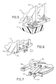
- FIG. 5 there is shown a leg member 43′ in accordance with an alternative embodiement of the invention.
- Leg 43′ as shown, extends downwardly from the heat sink's body segment 45 but in a direction substantially orthogonal to the parallel planes occupied by the heat sink's upwardly projecting fins 47.
- a total of four such legs 43′ are utilized.
- all four of such legs extends in this substantially orthogonal manner while also occupying opposingly oriented pairs.
- these legs are also in two adjacent pairs as in FIG. 3, with each of those legs in a respective pair projecting opposite to the other.
- each of the leg members of the invention engage the designated surface 27 of substrate 11 at a spaced location (distance) from the flexible, second circuitized substrate 15. See especially Figs. 1 & 2.
- the invention's pliant means does not, therefore, contact the flexible substrate during depression of the heat sink 17.
- stop means 71 which may also be utilized in the instant invention for the purpose of defining the predetermined distance that heat sink 17 may be depressed relative to substrate 11.
- stop means 71 comprises a projection 73 which extends downwardly from the end (or side) wall of the heat sink below the planar bottom surface 19. Understandably, the bottom edge of this stop means is designed for engaging the upper surface of substrate 11.
- stop means 71 preferably comprises an integral part of the heat sink's end wall. Understandably, stop means 71 extends downwardly a distance slightly greater than the thickness of chip 13, adhesive 33 and substrate 15 (and encapsulant 35, if used). In one example of the invention, stop 17 extended downwardly a total distance of 838,2 ⁇ m (0.033 inch).
- leg member 43 ⁇ in accordance with an alternative embodiment of the invention.
- leg member 43 ⁇ includes a bifurcated body portion 75 including two separate, elongated projecting leg segments 77 and 77′ which in turn define an elongated, internal slot 79 which extends substantially the entire length of the leg's body portion.
- This elongated, bifurcated configuration even further promotes formation of the aforementioned adhesive "rivet" to thus fixedly secure the heat sink to the rigid, bottom substrate 11.
- leg 84 includes an aperture 85 within the tapered body portion thereof.
- the aforedefined adhesive (not shown) will be forced up through the aperture and over onto the body portion's top surface, also forming a "rivet" to assist in fixedly securing the leg in final position.
- FIG. 9 there is shown yet another embodiment of a leg member 43′′′ adapted for use in the invention.
- Leg member 43′′′ is shown as projecting externally from heat sink 17 in a manner substantially opposite to the legs of the invention as depicted in FIGS. 1-3.
- leg 43′′′ projects in a substantially orthogonal, downward manner relative to the parallel, spaced fins 47.
- each leg is formed from a projecting flange which extends from the heat sink, the remainder of the flange being removed (e.g., cut away) following such leg formation.
- heat sink 17 would include two opposed flanges with a pair of leg members 43′′′ formed from each flange. This arrangement assures full coverage of the flexible substrate 15 such that the outer edge 87 of the heat sink substantially aligns with the corresponding outer edge 89 of substrate 15 located thereunder.
Landscapes
- Cooling Or The Like Of Semiconductors Or Solid State Devices (AREA)
Applications Claiming Priority (2)
| Application Number | Priority Date | Filing Date | Title |
|---|---|---|---|
| US07/218,726 US4849856A (en) | 1988-07-13 | 1988-07-13 | Electronic package with improved heat sink |
| US218726 | 1998-12-22 |
Publications (3)
| Publication Number | Publication Date |
|---|---|
| EP0350588A2 true EP0350588A2 (de) | 1990-01-17 |
| EP0350588A3 EP0350588A3 (de) | 1991-01-16 |
| EP0350588B1 EP0350588B1 (de) | 1995-02-01 |
Family
ID=22816259
Family Applications (1)
| Application Number | Title | Priority Date | Filing Date |
|---|---|---|---|
| EP89108553A Expired - Lifetime EP0350588B1 (de) | 1988-07-13 | 1989-05-12 | Elektronische Packung mit verbesserter Wärmesenke |
Country Status (5)
| Country | Link |
|---|---|
| US (1) | US4849856A (de) |
| EP (1) | EP0350588B1 (de) |
| JP (1) | JPH0712069B2 (de) |
| CA (1) | CA1290074C (de) |
| DE (1) | DE68920923T2 (de) |
Cited By (2)
| Publication number | Priority date | Publication date | Assignee | Title |
|---|---|---|---|---|
| US6055158A (en) * | 1999-03-16 | 2000-04-25 | Framatome Connectors Interlock, Inc. | Electronic component heat sink assembly |
| US6154367A (en) * | 1999-03-16 | 2000-11-28 | Framatome Connectors Interlock, Inc. | Heat sink for printed circuit board |
Families Citing this family (75)
| Publication number | Priority date | Publication date | Assignee | Title |
|---|---|---|---|---|
| US4970579A (en) * | 1988-09-21 | 1990-11-13 | International Business Machines Corp. | Integrated circuit package with improved cooling means |
| JPH02122759A (ja) * | 1988-10-31 | 1990-05-10 | Fuji Xerox Co Ltd | 画像記録装置の放熱装置 |
| US5028984A (en) * | 1988-11-04 | 1991-07-02 | International Business Machines Corporation | Epoxy composition and use thereof |
| US4960634A (en) * | 1990-03-14 | 1990-10-02 | International Business Machines Corporation | Epoxy composition of increased thermal conductivity and use thereof |
| US5031029A (en) * | 1990-04-04 | 1991-07-09 | International Business Machines Corporation | Copper device and use thereof with semiconductor devices |
| US5003429A (en) * | 1990-07-09 | 1991-03-26 | International Business Machines Corporation | Electronic assembly with enhanced heat sinking |
| US5057969A (en) * | 1990-09-07 | 1991-10-15 | International Business Machines Corporation | Thin film electronic device |
| US5107330A (en) * | 1990-10-19 | 1992-04-21 | At&T Bell Laboratories | Self-adjusting heat sink design for vlsi packages |
| US5132875A (en) * | 1990-10-29 | 1992-07-21 | Compaq Computer Corporation | Removable protective heat sink for electronic components |
| US5099393A (en) * | 1991-03-25 | 1992-03-24 | International Business Machines Corporation | Electronic package for high density applications |
| US5059129A (en) * | 1991-03-25 | 1991-10-22 | International Business Machines Corporation | Connector assembly including bilayered elastomeric member |
| DE4111247C3 (de) * | 1991-04-08 | 1996-11-21 | Export Contor Ausenhandelsgese | Schaltungsanordnung |
| US5203075A (en) * | 1991-08-12 | 1993-04-20 | Inernational Business Machines | Method of bonding flexible circuit to cicuitized substrate to provide electrical connection therebetween using different solders |
| US5311395A (en) * | 1992-10-29 | 1994-05-10 | Ncr Corporation | Surface mount heat sink |
| US5299090A (en) * | 1993-06-29 | 1994-03-29 | At&T Bell Laboratories | Pin-fin heat sink |
| US5654587A (en) * | 1993-07-15 | 1997-08-05 | Lsi Logic Corporation | Stackable heatsink structure for semiconductor devices |
| US5467251A (en) * | 1993-10-08 | 1995-11-14 | Northern Telecom Limited | Printed circuit boards and heat sink structures |
| US5693981A (en) * | 1993-12-14 | 1997-12-02 | Lsi Logic Corporation | Electronic system with heat dissipating apparatus and method of dissipating heat in an electronic system |
| US5514327A (en) * | 1993-12-14 | 1996-05-07 | Lsi Logic Corporation | Powder metal heat sink for integrated circuit devices |
| US5410451A (en) * | 1993-12-20 | 1995-04-25 | Lsi Logic Corporation | Location and standoff pins for chip on tape |
| US5673479A (en) * | 1993-12-20 | 1997-10-07 | Lsi Logic Corporation | Method for mounting a microelectronic circuit peripherally-leaded package including integral support member with spacer |
| US6008991A (en) * | 1993-12-20 | 1999-12-28 | Lsi Logic Corporation | Electronic system including packaged integrated circuits with heat spreading standoff support members |
| US5434105A (en) * | 1994-03-04 | 1995-07-18 | National Semiconductor Corporation | Process for attaching a lead frame to a heat sink using a glob-top encapsulation |
| US5583378A (en) * | 1994-05-16 | 1996-12-10 | Amkor Electronics, Inc. | Ball grid array integrated circuit package with thermal conductor |
| JPH0846098A (ja) * | 1994-07-22 | 1996-02-16 | Internatl Business Mach Corp <Ibm> | 直接的熱伝導路を形成する装置および方法 |
| US5504652A (en) * | 1994-09-16 | 1996-04-02 | Apple Computer, Inc. | Unitary heat sink for integrated circuits |
| US5923538A (en) * | 1994-10-17 | 1999-07-13 | Lsi Logic Corporation | Support member for mounting a microelectronic circuit package |
| US5557501A (en) * | 1994-11-18 | 1996-09-17 | Tessera, Inc. | Compliant thermal connectors and assemblies incorporating the same |
| US5757620A (en) * | 1994-12-05 | 1998-05-26 | International Business Machines Corporation | Apparatus for cooling of chips using blind holes with customized depth |
| US5604978A (en) * | 1994-12-05 | 1997-02-25 | International Business Machines Corporation | Method for cooling of chips using a plurality of materials |
| WO1996023397A1 (en) * | 1995-01-25 | 1996-08-01 | Northern Telecom Limited | Printed circuit board and heat sink arrangement |
| US5646826A (en) * | 1995-01-26 | 1997-07-08 | Northern Telecom Limited | Printed circuit board and heat sink arrangement |
| US5685071A (en) * | 1995-06-05 | 1997-11-11 | Hughes Electronics | Method of constructing a sealed chip-on-board electronic module |
| US5805418A (en) * | 1996-02-22 | 1998-09-08 | Cray Research, Inc. | Cooling cap method and apparatus for tab packaged integrated circuits |
| US5825625A (en) * | 1996-05-20 | 1998-10-20 | Hewlett-Packard Company | Heat conductive substrate mounted in PC board for transferring heat from IC to heat sink |
| US5730210A (en) * | 1997-02-24 | 1998-03-24 | Silicon Integrated Systems Corporation | Heat sink having an assembling device |
| KR100320983B1 (ko) * | 1997-08-22 | 2002-06-20 | 포만 제프리 엘 | 칩조립체및직접적인개방열전도성경로의제공방법 |
| US5966290A (en) * | 1997-09-03 | 1999-10-12 | Internatioinal Business Machines Corporation | Electronic packages and a method to improve thermal performance of electronic packages |
| US5960535A (en) * | 1997-10-28 | 1999-10-05 | Hewlett-Packard Company | Heat conductive substrate press-mounted in PC board hole for transferring heat from IC to heat sink |
| US6060341A (en) * | 1998-01-12 | 2000-05-09 | International Business Machines Corporation | Method of making an electronic package |
| US6429530B1 (en) | 1998-11-02 | 2002-08-06 | International Business Machines Corporation | Miniaturized chip scale ball grid array semiconductor package |
| AU713440B3 (en) * | 1999-05-25 | 1999-12-02 | First International Computer, Inc. | A support structure for a central processing unit |
| US6366461B1 (en) | 1999-09-29 | 2002-04-02 | Silicon Graphics, Inc. | System and method for cooling electronic components |
| US6822867B2 (en) | 2001-06-29 | 2004-11-23 | Intel Corporation | Electronic assembly with solderable heat sink and methods of manufacture |
| US20030131975A1 (en) * | 2002-01-11 | 2003-07-17 | Sabina Houle | Integrated heat spreader with mechanical interlock designs |
| US20050019656A1 (en) * | 2002-03-22 | 2005-01-27 | Yoon Sang Young | Method for fabricating composite electrodes |
| US20030180624A1 (en) * | 2002-03-22 | 2003-09-25 | Bookeun Oh | Solid polymer electrolyte and method of preparation |
| US7226702B2 (en) | 2002-03-22 | 2007-06-05 | Quallion Llc | Solid polymer electrolyte and method of preparation |
| US7498102B2 (en) * | 2002-03-22 | 2009-03-03 | Bookeun Oh | Nonaqueous liquid electrolyte |
| US7695860B2 (en) * | 2002-03-22 | 2010-04-13 | Quallion Llc | Nonaqueous liquid electrolyte |
| ATE543240T1 (de) * | 2002-05-16 | 2012-02-15 | Abb Schweiz Ag | Kühlelement |
| US6707676B1 (en) * | 2002-08-30 | 2004-03-16 | Ehood Geva | Heat sink for automatic assembling |
| US7588859B1 (en) | 2004-02-11 | 2009-09-15 | Bookeun Oh | Electrolyte for use in electrochemical devices |
| US8076031B1 (en) | 2003-09-10 | 2011-12-13 | West Robert C | Electrochemical device having electrolyte including disiloxane |
| US8076032B1 (en) | 2004-02-04 | 2011-12-13 | West Robert C | Electrolyte including silane for use in electrochemical devices |
| US7718321B2 (en) * | 2004-02-04 | 2010-05-18 | Quallion Llc | Battery having electrolyte including organoborate salt |
| US20070065728A1 (en) | 2003-03-20 | 2007-03-22 | Zhengcheng Zhang | Battery having electrolyte with mixed solvent |
| US20050039884A1 (en) * | 2003-08-20 | 2005-02-24 | Ivan Pawlenko | Conformal heat sink |
| US7473491B1 (en) | 2003-09-15 | 2009-01-06 | Quallion Llc | Electrolyte for electrochemical cell |
| US8765295B2 (en) | 2004-02-04 | 2014-07-01 | Robert C. West | Electrolyte including silane for use in electrochemical devices |
| US9786954B2 (en) | 2004-02-04 | 2017-10-10 | Robert C. West | Electrolyte including silane for use in electrochemical devices |
| US8153307B1 (en) | 2004-02-11 | 2012-04-10 | Quallion Llc | Battery including electrolyte with mixed solvent |
| US7327025B2 (en) * | 2004-04-30 | 2008-02-05 | St Assembly Test Services Ltd. | Heat spreader for thermally enhanced semiconductor package |
| US7561436B2 (en) * | 2005-06-06 | 2009-07-14 | Delphi Technologies, Inc. | Circuit assembly with surface-mount IC package and heat sink |
| US20060273824A1 (en) * | 2005-06-06 | 2006-12-07 | Sauer-Danfoss Inc. | High current switching circuit for a motor drive three phase inverter for mobile equipment |
| US7709951B2 (en) * | 2007-03-16 | 2010-05-04 | International Business Machines Corporation | Thermal pillow |
| TWI338939B (en) * | 2007-08-15 | 2011-03-11 | Via Tech Inc | Package module and electronic device |
| US8362609B1 (en) | 2009-10-27 | 2013-01-29 | Xilinx, Inc. | Integrated circuit package and method of forming an integrated circuit package |
| US8567483B2 (en) * | 2009-11-06 | 2013-10-29 | International Business Machines Corporation | Heatsink with flexible base and height-adjusted cooling fins |
| US8810028B1 (en) | 2010-06-30 | 2014-08-19 | Xilinx, Inc. | Integrated circuit packaging devices and methods |
| ITMI20111214A1 (it) | 2011-06-30 | 2012-12-31 | St Microelectronics Srl | Dispositivo di potenza a spessore ridotto |
| ITMI20111217A1 (it) * | 2011-06-30 | 2012-12-31 | St Microelectronics Srl | Sistema contenitore/dissipatore per componente elettronico |
| US10043619B2 (en) | 2014-03-28 | 2018-08-07 | Black & Decker Inc. | Biasing member for a power tool forward/reverse actuator |
| JP2017127097A (ja) | 2016-01-13 | 2017-07-20 | 株式会社デンソー | 制御装置一体型回転電機 |
| US10541588B2 (en) | 2017-05-24 | 2020-01-21 | Black & Decker Inc. | Electronic power module for a power tool having an integrated heat sink |
Family Cites Families (13)
| Publication number | Priority date | Publication date | Assignee | Title |
|---|---|---|---|---|
| US3670215A (en) * | 1970-09-28 | 1972-06-13 | Staver Co Inc The | Heat dissipator for integrated circuit |
| NL159818B (nl) * | 1972-04-06 | 1979-03-15 | Philips Nv | Halfgeleiderinrichting, bevattende een flexibele isolerende folie, die aan een zijde is voorzien van metalen geleider- sporen. |
| US4066839A (en) * | 1972-11-16 | 1978-01-03 | Sgs-Ates Componenti Elettronici S.P.A. | Molded body incorporating heat dissipator |
| US4012768A (en) * | 1975-02-03 | 1977-03-15 | Motorola, Inc. | Semiconductor package |
| US4004195A (en) * | 1975-05-12 | 1977-01-18 | Rca Corporation | Heat-sink assembly for high-power stud-mounted semiconductor device |
| JPS5772357A (en) * | 1980-10-24 | 1982-05-06 | Nec Corp | Mounting method of integrated circuit |
| US4415025A (en) * | 1981-08-10 | 1983-11-15 | International Business Machines Corporation | Thermal conduction element for semiconductor devices |
| JPS5972739U (ja) * | 1982-11-04 | 1984-05-17 | 富士通株式会社 | 放熱フイン |
| US4593342A (en) * | 1984-11-15 | 1986-06-03 | General Electric Company | Heat sink assembly for protecting pins of electronic devices |
| US4605058A (en) * | 1985-04-01 | 1986-08-12 | The Staver Company, Inc. | Heat dissipating retainer for electronic package |
| US4658331A (en) * | 1985-09-09 | 1987-04-14 | Tektronix, Inc. | Mounting an integrated circuit chip to an etched circuit board |
| US4750089A (en) * | 1985-11-22 | 1988-06-07 | Texas Instruments Incorporated | Circuit board with a chip carrier and mounting structure connected to the chip carrier |
| WO1989008327A1 (en) * | 1988-03-01 | 1989-09-08 | Digital Equipment Corporation | Method and apparatus for packaging and cooling integrated circuit chips |
-
1988
- 1988-07-13 US US07/218,726 patent/US4849856A/en not_active Expired - Lifetime
-
1989
- 1989-04-20 JP JP1099045A patent/JPH0712069B2/ja not_active Expired - Lifetime
- 1989-05-12 DE DE68920923T patent/DE68920923T2/de not_active Expired - Fee Related
- 1989-05-12 EP EP89108553A patent/EP0350588B1/de not_active Expired - Lifetime
- 1989-05-18 CA CA000600081A patent/CA1290074C/en not_active Expired - Lifetime
Cited By (2)
| Publication number | Priority date | Publication date | Assignee | Title |
|---|---|---|---|---|
| US6055158A (en) * | 1999-03-16 | 2000-04-25 | Framatome Connectors Interlock, Inc. | Electronic component heat sink assembly |
| US6154367A (en) * | 1999-03-16 | 2000-11-28 | Framatome Connectors Interlock, Inc. | Heat sink for printed circuit board |
Also Published As
| Publication number | Publication date |
|---|---|
| EP0350588B1 (de) | 1995-02-01 |
| JPH0240941A (ja) | 1990-02-09 |
| JPH0712069B2 (ja) | 1995-02-08 |
| DE68920923T2 (de) | 1995-08-10 |
| EP0350588A3 (de) | 1991-01-16 |
| DE68920923D1 (de) | 1995-03-16 |
| CA1290074C (en) | 1991-10-01 |
| US4849856A (en) | 1989-07-18 |
Similar Documents
| Publication | Publication Date | Title |
|---|---|---|
| EP0350588B1 (de) | Elektronische Packung mit verbesserter Wärmesenke | |
| US7851906B2 (en) | Flexible circuit electronic package with standoffs | |
| EP0948814B1 (de) | Lötballgitter in chipgrösse für integrierte schaltungspackung | |
| US5866949A (en) | Chip scale ball grid array for integrated circuit packaging | |
| US5677575A (en) | Semiconductor package having semiconductor chip mounted on board in face-down relation | |
| US5760465A (en) | Electronic package with strain relief means | |
| TWI459513B (zh) | 半導體封裝及其製作方法 | |
| KR101694657B1 (ko) | 방열 구조를 갖는 반도체 패키지 | |
| US5359768A (en) | Method for mounting very small integrated circuit package on PCB | |
| GB2286084A (en) | Electronic package with thermally conductive support | |
| EP0553463A1 (de) | Elektronikverpackung mit erhöhter Wärmeableitung und Verfahren zu ihrer Herstellung | |
| JPH06260532A (ja) | フリップチップの接続構造 | |
| EP0546285A1 (de) | Elektronische Baugruppe mit schützendem Verkapselungsmaterial | |
| JP3094768B2 (ja) | 半導体装置 | |
| JPH08186151A (ja) | 半導体装置及びその製造方法 | |
| JP3370498B2 (ja) | 半導体装置用基板 | |
| JPH1065042A (ja) | 半導体装置 | |
| US6875635B2 (en) | Method of attaching a die to a substrate | |
| JPH11126795A (ja) | 実装基板およびその製造方法ならびに電子部品の実装方法 | |
| JPH0513647A (ja) | 半導体装置 | |
| JP3348485B2 (ja) | 半導体装置と実装基板 | |
| JP2000243871A (ja) | 回路基板 | |
| JPH09111204A (ja) | 導電性接着テープおよびこれを用いた半導体装置用パッケージ | |
| JPH08153828A (ja) | 半導体装置用パッケージ | |
| JP2000133743A (ja) | 半導体チップの実装構造、およびこれを備えた半導体装置 |
Legal Events
| Date | Code | Title | Description |
|---|---|---|---|
| PUAI | Public reference made under article 153(3) epc to a published international application that has entered the european phase |
Free format text: ORIGINAL CODE: 0009012 |
|
| AK | Designated contracting states |
Kind code of ref document: A2 Designated state(s): DE FR GB IT |
|
| 17P | Request for examination filed |
Effective date: 19900512 |
|
| PUAL | Search report despatched |
Free format text: ORIGINAL CODE: 0009013 |
|
| AK | Designated contracting states |
Kind code of ref document: A3 Designated state(s): DE FR GB IT |
|
| RHK1 | Main classification (correction) |
Ipc: H01L 23/367 |
|
| 17Q | First examination report despatched |
Effective date: 19930401 |
|
| GRAA | (expected) grant |
Free format text: ORIGINAL CODE: 0009210 |
|
| AK | Designated contracting states |
Kind code of ref document: B1 Designated state(s): DE FR GB IT |
|
| PG25 | Lapsed in a contracting state [announced via postgrant information from national office to epo] |
Ref country code: IT Free format text: LAPSE BECAUSE OF FAILURE TO SUBMIT A TRANSLATION OF THE DESCRIPTION OR TO PAY THE FEE WITHIN THE PRESCRIBED TIME-LIMIT;WARNING: LAPSES OF ITALIAN PATENTS WITH EFFECTIVE DATE BEFORE 2007 MAY HAVE OCCURRED AT ANY TIME BEFORE 2007. THE CORRECT EFFECTIVE DATE MAY BE DIFFERENT FROM THE ONE RECORDED. Effective date: 19950201 |
|
| REF | Corresponds to: |
Ref document number: 68920923 Country of ref document: DE Date of ref document: 19950316 |
|
| PGFP | Annual fee paid to national office [announced via postgrant information from national office to epo] |
Ref country code: FR Payment date: 19950427 Year of fee payment: 7 |
|
| ET | Fr: translation filed | ||
| PLBE | No opposition filed within time limit |
Free format text: ORIGINAL CODE: 0009261 |
|
| STAA | Information on the status of an ep patent application or granted ep patent |
Free format text: STATUS: NO OPPOSITION FILED WITHIN TIME LIMIT |
|
| 26N | No opposition filed | ||
| PGFP | Annual fee paid to national office [announced via postgrant information from national office to epo] |
Ref country code: GB Payment date: 19960422 Year of fee payment: 8 |
|
| PG25 | Lapsed in a contracting state [announced via postgrant information from national office to epo] |
Ref country code: FR Effective date: 19970131 |
|
| REG | Reference to a national code |
Ref country code: FR Ref legal event code: ST |
|
| PG25 | Lapsed in a contracting state [announced via postgrant information from national office to epo] |
Ref country code: GB Effective date: 19970512 |
|
| PGFP | Annual fee paid to national office [announced via postgrant information from national office to epo] |
Ref country code: DE Payment date: 19970521 Year of fee payment: 9 |
|
| GBPC | Gb: european patent ceased through non-payment of renewal fee |
Effective date: 19970512 |
|
| PG25 | Lapsed in a contracting state [announced via postgrant information from national office to epo] |
Ref country code: DE Free format text: LAPSE BECAUSE OF NON-PAYMENT OF DUE FEES Effective date: 19990302 |