EP0350928A2 - Processeur de données capable d'exécuter la division de données à signes en un petit nombre d'étapes de programme - Google Patents
Processeur de données capable d'exécuter la division de données à signes en un petit nombre d'étapes de programme Download PDFInfo
- Publication number
- EP0350928A2 EP0350928A2 EP89112866A EP89112866A EP0350928A2 EP 0350928 A2 EP0350928 A2 EP 0350928A2 EP 89112866 A EP89112866 A EP 89112866A EP 89112866 A EP89112866 A EP 89112866A EP 0350928 A2 EP0350928 A2 EP 0350928A2
- Authority
- EP
- European Patent Office
- Prior art keywords
- data
- divisor
- sign
- dividend
- complement
- Prior art date
- Legal status (The legal status is an assumption and is not a legal conclusion. Google has not performed a legal analysis and makes no representation as to the accuracy of the status listed.)
- Granted
Links
Images


Classifications
-
- G—PHYSICS
- G06—COMPUTING OR CALCULATING; COUNTING
- G06F—ELECTRIC DIGITAL DATA PROCESSING
- G06F7/00—Methods or arrangements for processing data by operating upon the order or content of the data handled
- G06F7/38—Methods or arrangements for performing computations using exclusively denominational number representation, e.g. using binary, ternary, decimal representation
- G06F7/48—Methods or arrangements for performing computations using exclusively denominational number representation, e.g. using binary, ternary, decimal representation using non-contact-making devices, e.g. tube, solid state device; using unspecified devices
- G06F7/52—Multiplying; Dividing
- G06F7/535—Dividing only
-
- G—PHYSICS
- G06—COMPUTING OR CALCULATING; COUNTING
- G06F—ELECTRIC DIGITAL DATA PROCESSING
- G06F9/00—Arrangements for program control, e.g. control units
- G06F9/06—Arrangements for program control, e.g. control units using stored programs, i.e. using an internal store of processing equipment to receive or retain programs
- G06F9/30—Arrangements for executing machine instructions, e.g. instruction decode
- G06F9/30003—Arrangements for executing specific machine instructions
- G06F9/30007—Arrangements for executing specific machine instructions to perform operations on data operands
- G06F9/3001—Arithmetic instructions
-
- G—PHYSICS
- G06—COMPUTING OR CALCULATING; COUNTING
- G06F—ELECTRIC DIGITAL DATA PROCESSING
- G06F2207/00—Indexing scheme relating to methods or arrangements for processing data by operating upon the order or content of the data handled
- G06F2207/535—Indexing scheme relating to groups G06F7/535 - G06F7/5375
- G06F2207/5353—Restoring division
Definitions
- the present invention relates to a data processor, and more specifically to a system for executing a division of signed data in a microprogram controlled microcomputer.
- microprogram controlled microcomputers have an instruction execution unit composed of a temporary register group having a shift function and used for temporarily storing items of operand data such as a dividend, a divisor, etc., an arithmetic logic unit (ALU), a so called SS flag indicative of an exclusive-OR between respective signs of the dividend and the divisor stored in the temporary register group, a so called SD flag showing the sign of the divisor, and a microsequencer controlling an overall operation of the execution unit. Information hold in the SS flag and the SD flag is supplied to the microsequencer.
- ALU arithmetic logic unit
- the microsequencer controls to transfer a dividend data and a divisor data to the temporary register group, and to set the sign data to the SS flag and SD flag.
- the microsequencer examines a most significant bit (MSB) of the dividend, and if the MSB of the dividend is "1" which indicates that the dividend is negative, a branch processing is stated in the microprogram, so that the ALU generates a two's complement of the dividend.
- MSB most significant bit
- the microsequencer examines a MSB bit of the divisor, and if the MSB of the divisor is "1" which indicates that the divisor is negative, a branch processing is also started in the microprogram, so that the ALU generates a two's complement of the divisor. As the result of the above processing, the dividend and the divisor in the form of an absolute value are obtained.
- a division operation of the dividend by the divisor is executed in accordance with a so-called restoring method by utilizing the shift function of the temporary register group and the ALU.
- a quotient is stored in the temporary register group, and the microsequencer corrects a sign of the quotient with reference to a content of the SS flag as follows:
- Another object of the present invention is to provide a data processor capable of executing a division of signed data with decreased microprogram steps and at an increased operation speed.
- a data processor comprising data storage means for temporarily storing a dividend data and a divisor data, sign information storage means coupled to the data storage means for detecting a sign of each of the dividend data and the divisor data and storing the detected sign information, arithmetic and logic operation execution means coupled to the data storage means and having an arithmetic logic operation function required for execution of a division operation and a two's compliment obtaining operation, instruction execution control means coupled to the arithmetic and logic operation execution means for controlling the arithmetic and logic operation execution means so as to cause the arithmetic and logic operation execution means to selectively execute a given instruction, the instruction execution control means generating a two's complement obtaining operation instruction signal, and operation control means coupled to the sign information storage means and to receive the two's complement obtaining operation instruction signal and operating to control the arithmetic and logic operation execution means in accordance with an output of the sign information storage means so as to cause the a
- the execution unit 100 is generally indicated by Reference Numeral 100, which includes a microsequencer 10 associated with a microprogram memory 12 and adapted to read a required microprogram from the microprogram memory 12.
- the microsequencer 10 is also coupled to an instruction bus 14 of M bits to receive a given instruction through the instruction bus 14.
- the microsequencer 10 reads a microprogram from the associated microprogram memory 12, and generates various control signals as the result of decoding of the microprogram.
- Only signals required for execution of the division of signed data are shown in Figure 1, and will be explained in the following description.
- the execution unit 100 also includes a data bus 16 of N bits, a temporary register set 18 coupled to the data bus 16, and an arithmetic logic unit (ALU) 20 having a pair of N-bit inputs connected to the temporary register set 18 and an N-bit output connected to the data bus 16
- the temporary register set 18 includes a divisor register 22, a dividend/quotient register 24 and a remainder register 26.
- a most significant bit (MSB) of the data bus 16 and a MSB bit of the divisor register 22 are connected through lines 28 and 30 to a sign detector circuit 32, respectively.
- the sign detection circuit 32 generates three sign signals SD, SA and SS to a divisor sign flag (SD flag) 34, a dividend sign flag (SA flag) 36 and a quotient sign flag (SS flag) 38, respectively.
- Output SDO, SAO and SSO of these flags 34, 36 and 38 are connected through lines 40, 42 and 44 to a correction operation control circuit 46, which is also connected to receive a divisor/remainder two's complement data generation instruction signal SDC, a dividend two's complement data generation instruction signal SAC and a quotient two's complement data generation instruction signal SSC, through lines 48, 50 and 52 from the microsequencer 10, respectively.
- the SDC signal, the SAC signal and the SSC signal are furthermore supplied to the temporary register set 18.
- the correction operation control circuit 46 generates an operation invalidation signal IVD and a complement obtaining operation signal COD, which are supplied through lines 54 and 56 to the ALU 20.
- the microsequencer 10 outputs an operation mode designation signal ODS through a bus 58 of L bits to the ALU 20, and also generates a divisor write signal DSW, a dividend write signal DDW, a quotient write signal QW, a remainder write signal RW, an RD flag write signal SDW and an SA/SS flag write signal SSAW.
- the DSW signal, the DDW signal, the QW signal and the RW signal are supplied to the temporary register set 18 through lines 60, 62, 64 and 66, respectively.
- the DDW signal and the DSW signal are also supplied to the sign detection circuit 32.
- the SDW is supplied to the SD flag 34, and the SSAW signal is supplied to the SA flag 36 and the SS flag 38.
- a data memory 68 and a general purpose registers 70 are connected to the data bus 16.
- the divisor register 22 of the temporary register set 18 are used to temporarily store a divisor supplied on the data bus 16, in response to the DSW signal which is generated by the microsequencer 10 when the divisor should be written from the data bus 16 to the divisor register 22.
- the dividend/quotient register 24 of the temporary register set 18 is used to temporarily store a dividend supplied on the data bus 16, in response to the DDW signal which is generated by the microsequencer 10.
- the remainder register 26 is used to temporarily store a remainder generated as the result of the division operation.
- the dividend/quotient register 24 is also used to store a quotient as the result of the division operation.
- at least the registers 24 and 26 have a data shift function.
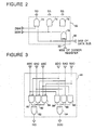
- the sign detection circuit 32 is composed of three AND gates 72, 74 and 76 and one exclusive-OR gate 78, which are connected as shown in Figure 2.
- the AND gate 72 has a first input connected to receive the MSB bit of the data bus 16 through the line 28, and a second input connected to receive the DSW signal from the microsequencer 10. Therefore, when the divisor is written to the divisor register 22, the AND gate 72 outputs the MSB bit of the data bus, namely the sign of the divisor, as a divisor sign information SD.
- the divisor sign information SD is written to the SD flag 34 in response to the SDW signal from the microprocessor 10.
- the AND gate 74 has a first input connected to receive the MSB bit of the data bus 16 through the line 28, and a second input connected to receive the DDW signal from the microsequencer 10. Therefore, when the dividend is written to the dividend register 24, the AND gate 74 outputs the MSB bit of the data bus, namely the sign of the dividend, as a dividend sign information SA.
- the dividend sign information SA is written to the SA flag 36 in response to the SSAW signal from the microsequencer 10.
- the exclusive-OR gate 78 has a first input connected to receive the MSB bit of the data bus 16 through the line 28, and a second input connected to receive the MSB bit of the divisor register 22 through the line 30. An output of the exclusive-OR gate 78 is connected to a first input of the AND gate 76, whose second input is connected to receive the DDW signal from the microsequencer. Therefore, when the dividend is written to the dividend register 24, the exclusive-OR between the MSB or sign bit of the divisor held in the divisor register 22 and the MSB or sign bit of the dividend on the data bus 16 is generated by the exclusive-OR gate 78, and outputted through the AND gate 76 in response to the SSAW signal from the microprocessor 10.
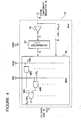
- the correction operation control circuit 46 which receives the SDO signal, the SAO signal and the SSO signal from the three flags 34,36 and 38 and the SDC signal, the SAC signal and the SSC signal from the microsequencer 10, includes six AND gates 80, 82, 84, 86, 88 and 90 and two three-input OR gates 92 and 94, connected as shown in Figure 3.
- the AND gate 80 has a first and non-inverted input connected to receive the SDC signal and a second and inverted input connected to receive the SDO signal.
- the AND gate 82 has a first and non-inverted input connected to receive the SAC signal and a second and inverted input connected to receive the SAO signal.
- the AND gate 84 has a first and non-inverted input connected to receive the SSC signal and a second and inverted input connected to receive the SSO signal.
- Three inputs of the OR gate 92 are connected to outputs of the three AND gates 80, 82 and 84, respectively, so that the OR gate 92 generates the operation invalidation signal IVD.
- Two inputs of the AND gate 86 are connected to receive the SDC signal and the SDO signal, respectively, and two inputs of the AND gate 88 are connected to receive the SAC signal and the SAO signal, respectively.
- the AND gate 90 has two inputs connected to receive the SSC signal and the SSO signal, respectively.
- Three inputs of the OR gate 94 are connected to outputs of the three AND gates 86, 88 and 90, respectively, so that the OR gate 94 generates complement obtaining operation signal COD.
- the ALU 20 is controlled by the operation mode designation signal ODS supplied through the L-bit bus 58 from the microsequencer 10, so that the ALU 20 executes either a monadic operation for one item of data supplied from the temporary register set 18 or a dyadic operation for two items of data supplied from the temporary register set 18.
- ODS operation mode designation signal
- the ALU 20 assumes an equivalent circuit as shown in Figure 4. Namely, an N-bit data (B0-B N-1 ) supplied from the temporary register 18 is inverted by an N-bit inverter 96, and fed to an incrementer 97 where the inverted data is added with +1.
- the incrementer 97 outputs a two's complement data (CB0-CB N-1 ) of the data supplied from the temporary register 18.
- the two's complement data (CB0-CB N-1 ) is supplied to one input of a multiplexor 98, whose another input is connected to receive the N-bit data (B0-B N-1 ) supplied from the temporary register 18.
- the multiplexor 98 includes an N-number of AND gates 98A having their first input connected to a corresponding bit of the two's complement data (CB0-CB N-1 ). Second inputs of all the AND gates 98A are commonly connected to receive the COD signal. Furthermore, the multiplexor 98 includes an N-number of AND gates 98B having their first input connected to a corresponding bit of the N-bit data (B0-B N-1 ) supplied from the temporary register 18. Second inputs of all the AND gates 98B are commonly connected to receive the IVD signal.
- Outputs of the AND gates 98A and 98B located at the same digit or place are connected to an OR gate 98C, and the outputs of all the OR gates 98C form a N-bit output data, which is supplied to the N-bit data bus 16.
- the AND gates 98A and 98B are controlled by the complement obtaining operation signal COD and the operation invalidation signal IVD, respectively. If the operation invalidation signal IVD is activated, the multiplexor 98 selects the N-bit data (B0-B N-1 ) supplied from the temporary register 18, so that the two's complement derived by cooperation of the invention 96 and the incrementer 97 is substantially invalidated. On the other hand, if the complement obtaining operation signal COD is activated, the multiplexor 98 selects the two's complement data (CB0-CB N-1 ), with the result that the ALU 20 executes the operation for deriving the two's complement data.
- the microsequencer 10 When a division instruction is given through the instruction bus 14 to the microsequencer 10, a microprogram required for execution of the division instruction is read from the associated microprogram memory 12, and is started by the microsequencer 10. In the microprogrammed processing for the division operation, the microsequencer 10 firstly controls to read a divisor and a dividend from the data memory 68 or the general purpose registers 70 through the data bus 16 and to write them to the divisor register 22 and the dividend/quotient register 24 of the temporary register set 18. In addition, the sign data of the divisor, the sign data of the dividend and the exclusive-OR therebetween are written to the flags 34, 36 and 38, respectively.
- the microsequencer 10 controls to cause a divisor to be output to the data bus 16
- the microsequencer 10 outputs an active divisor write signal DSW to the line 60 so as to cause the divisor on the data bus 16 to be written into the divisor register 22.
- the AND gate 72 is opened in response to the active DSW signal, so that the MSB of the data on the data bus 16 or the sign bit of the divisor is outputted from the AND gate 72 to the SD flag 34.
- the microsequencer 10 generates an active SD flag write signal SDW, so that the sign bit of the divisor is written to the SD flag 34.
- the microsequencer 10 controls to cause a dividend to be output to the data bus 16 on one hand, and outputs an active dividend write signal DSW to the line 62 on the other hand as shown in Figure 6, so that the dividend on the data bus 16 is written into the dividend/quotient register 24.
- the AND gates 74 and 76 are opened, so that the MSB of the data on the data bus 16 or the sign bit of the dividend is outputted from the AND gate 74, and the exclusive-OR between the sign bit of the divisor held in the divisor register 22 and the MSB of the data on the data bus 16 is outputted from the exclusive-OR gate 78 through the AND gate 76.
- the microsequencer 10 generates an active SA/SS flag write signal SSAW, so that the sign bit of the dividend is written to the SA flag 36, and the exclusive-OR between the respective sign bits of the divisor and the dividend is written to the SS flag 38.
- the microsequencer 10 In the course of writing the dividend to the register/quotient register 24, the microsequencer 10 also instructs an absolute value derivation of the divisor. Specifically, the microsequencer 10 outputs an operation mode designation signal ODS designating a two's complement obtaining operation, through the bus 58 to the ALU 20, and at the same time, the microsequencer 10 generates an active divisor's two's complement obtaining operation signal SDC in phase with the DDW signal, as seen from Figure 6. This SDC signal is inputted to the temporary register set 18 as a data read signal for reading and outputting a content of the divisor register 22 to the ALU 20. As a result, the divisor is supplied to the ALU 20.
- ODS operation mode designation signal
- SDC active divisor's two's complement obtaining operation signal
- the SDC signal supplied to the correction operation control circuit 46 is inputted to the AND gates 80 and 86, so that these AND gates are opened.
- the SDO signal of the SD flag 34 is "1”
- the output of the AND gate 86 is brought to "1”
- the two's complement obtaining operation signal COD is also brought to "1”.
- the operation invalidation signal IVD is maintained at "0”.
- the multiplexor 98 selects the two's complement of the divisor generated by the inverter 96 and the incrementer 97.
- the ALU 20 After the writing of the dividend into the dividend register 24 has been completed, namely, at a tailing edge of the DDW signal, the ALU 20 outputs the two's complement data of the divisor to the data bus 16, as shown in Figure 6. At this time, the microsequencer 10 generates the divisor write signal DSW, again, so that the two's complement data of the divisor, namely, the absolute value of the divisor is written to the divisor register 22.
- the microsequencer 10 also instructs an absolute value derivation of the dividend. Namely, the microsequencer 10 generates an active dividend's two's complement obtaining operation signal SAC in phase with the active DSW signal, as seen from Figure 6.
- This SAC signal is inputted to the temporary register set 18 as a data read signal for reading and outputting a content of the dividend/quotient register 24 to the ALU 20, so that the dividend is supplied to the ALU 20.
- the SAC signal is inputted to the AND gates 82 and 88 of the correction operation control circuit 46, so that these AND gates are opened.
- the multiplexor 98 selects the dividend outputted from the temporary register set 18. In other words, calculation of the two's complement of the dividend in the ALU 20 will be invalidated.
- the ALU 20 After the writing of the divisor's two's complement into the divisor register 22 has been completed, the ALU 20 outputs the dividend outputted from the temporary register set 18, to the data bus 16 without any modification, as shown in Figure 6. At this time, the microprocessor 10 generates the dividend write signal DDW, again, so that the the dividend on the data bus 16 is written to the dividend register 24.
- the absolute values of the divisor and the dividend have been prepared.
- the above mentioned embodiment has no microprogram step for detecting the sign information of the divisor and the dividend, on the other hand, and automatically determines whether an operation for deriving a two's complement for the purpose of obtaining an absolute value should be executed or invalidated, on the other hand.
- the number of microprocessor steps can be decreased, and the operation speed can be made higher.
- a division operation is executed for the divisor and the dividend expressed in the form of an absolute value.
- This division operation is executed by the restoring method by utilizing the shift function of the registers 24 and 26 and the ALU 20.
- the ALU 20 is controlled by the operation mode designation signal ODS from the microsequencer 10 so that the ALU 20 functions as a subtracter, and a quotient and a remainder generated as the result of the division operation are stored in the registers 24 and 26, respectively.
- the microsequencer 10 executes the correction of the signal of the obtained quotient in accordance with the value of the SS flag.
- the microsequencer supplies the ALU 20 with the operation mode designation signal ODS for instructing the two's complement obtaining operation mode, and generates an active quotient's two's complement obtaining instruction signal SSC, as shown in Figure 6.
- This SSC signal is inputted to the temporary register set 18 as a data read signal for reading and outputting a content of the dividend/quotient register 24 to the ALU 20, so that the quotient is supplied to the ALU 20.
- the SCC signal is also inputted to the AND gates 84 and 90 of the correction operation control circuit 46, so that these AND gates are opened.
- the multiplexor 98 selects the two's complement of the quotient.
- the ALU 20 outputs the two's complement of the quotient to the data bus 16.
- the microsequencer 10 generates the quotient write signal QW after the SSC signal falls down but while the COD signal is still acitve. This QW signal is supplied through the line 64 to the temporary register set 18, so that the two's complement of the quotient on the data bus 16 is written to the dividend/quotient register 24.
- the microsequencer 10 starts an operation for correction of the remainder on the basis of the value of the SD flag 34.
- the sign of the remainder can be corrected not only on the basis of the value of the SD flag (namely, the sign of the divisor) but also on the basis of the value of SA flag (namely, the sign of the dividend).
- the sign of the remainder is corrected on the basis of the SD flag or on the basis of the SA flag, cannot be uniformly determined, but is dependent upon an actual architecture of each data processor. In the shown example, the sign of the remainder is corrected on the basis of the SD flag.
- the microsequencer 10 generates the remainder's two's complement obtaining operation signal SDC in phase with the quotient write signal QW.
- the SDC signal is inputted to the temporary register set 18 as a data read signal for reading and outputting a content of the remainder register 26 to the ALU 20, so that the remainder is supplied to the ALU 20.
- the SDC signal supplied to the correction operation control circuit 46 is inputted to the AND gates 80 and 86, so that these AND gates are opened.
- the SDO signal of the SD flag 34 is "1"
- the output of the AND gate 86 is brought to "1"
- the two's complement obtaining operation signal COD is also brought to "1". Namely, the COD signal is maintained in an active condition.
- the multiplexor 98 selects the two's complement of the remainder generated by the inverter 96 and the incrementer 97, so that the two's complement of the remainder is outputted onto the data bus 16. Thereafter, in response to the remainder write signal RW from the microsequencer 10, the two's complement of the remainder on the data bus 16 is written to the remainder register 26.
- the sign corrections of the quotient and the remainder have been completed.
- the program step number can be decreased, and the operation speed can be improved.
- whether or not a two's complement obtaining operation should be executed is controlled by the correction operation control circuit 46 for all the divisor, the dividend, the quotient and the remainder.
- the two's complement obtaining operation may be limited to only the divisor and the dividend, or to only the quotient and the remainder.
- the data processor in accordance with the present invention is characterized by a combination of means for storing the sign data of the divisor and the dividend, with means responding to the sign data storing means for controlling whether or not a complement data operation instructing signal should be supplied to an ALU.
- the data processor in accordance with the present invention can execute the division operation of signed data with a reduced number of program steps and at an increased operation speed.
Landscapes
- Engineering & Computer Science (AREA)
- Physics & Mathematics (AREA)
- General Physics & Mathematics (AREA)
- Theoretical Computer Science (AREA)
- Mathematical Optimization (AREA)
- Pure & Applied Mathematics (AREA)
- Mathematical Analysis (AREA)
- Computational Mathematics (AREA)
- Software Systems (AREA)
- General Engineering & Computer Science (AREA)
- Computing Systems (AREA)
- Complex Calculations (AREA)
- Executing Machine-Instructions (AREA)
Applications Claiming Priority (2)
| Application Number | Priority Date | Filing Date | Title |
|---|---|---|---|
| JP175804/88 | 1988-07-13 | ||
| JP17580488 | 1988-07-13 |
Publications (3)
| Publication Number | Publication Date |
|---|---|
| EP0350928A2 true EP0350928A2 (fr) | 1990-01-17 |
| EP0350928A3 EP0350928A3 (fr) | 1991-11-06 |
| EP0350928B1 EP0350928B1 (fr) | 1997-01-22 |
Family
ID=16002532
Family Applications (1)
| Application Number | Title | Priority Date | Filing Date |
|---|---|---|---|
| EP89112866A Expired - Lifetime EP0350928B1 (fr) | 1988-07-13 | 1989-07-13 | Processeur de données capable d'exécuter la division de données à signes en un petit nombre d'étapes de programme |
Country Status (4)
| Country | Link |
|---|---|
| US (1) | US5107453A (fr) |
| EP (1) | EP0350928B1 (fr) |
| JP (1) | JP3098242B2 (fr) |
| DE (1) | DE68927691T2 (fr) |
Cited By (4)
| Publication number | Priority date | Publication date | Assignee | Title |
|---|---|---|---|---|
| FR2693571A1 (fr) * | 1992-07-13 | 1994-01-14 | Texas Instruments France | Système de traitement de données dont le programme de commande comporte des instructions dépendant de paramètres d'état. |
| EP0650613A1 (fr) * | 1992-07-13 | 1995-05-03 | Texas Instruments France | Systeme de traitement de donnees a dispositif de traitement de boucles de programme |
| EP0656584A1 (fr) * | 1993-11-30 | 1995-06-07 | Texas Instruments Incorporated | Chargement conditionnel de mémoire d'une paire de registres |
| EP0902358A3 (fr) * | 1991-06-24 | 2002-01-02 | Hitachi, Ltd. | Circuit et procédé de division |
Families Citing this family (6)
| Publication number | Priority date | Publication date | Assignee | Title |
|---|---|---|---|---|
| US5426600A (en) * | 1993-09-27 | 1995-06-20 | Hitachi America, Ltd. | Double precision division circuit and method for digital signal processor |
| US5754460A (en) * | 1995-05-26 | 1998-05-19 | National Semiconductor Corporation | Method for performing signed division |
| US5831877A (en) * | 1995-05-26 | 1998-11-03 | National Semiconductor Corporation | Bit searching through 8, 16, or 32 bit operands using a 32 bit data path |
| DE69626596T2 (de) * | 1995-10-20 | 2003-12-18 | Kabushiki Kaisha Toshiba, Kawasaki | Logische Schaltung, die nach dem Carry select Prinzip arbeitet |
| US7174358B2 (en) * | 2002-11-15 | 2007-02-06 | Broadcom Corporation | System, method, and apparatus for division coupled with truncation of signed binary numbers |
| US7165086B2 (en) * | 2002-11-15 | 2007-01-16 | Broadcom Corporation | System, method, and apparatus for division coupled with rounding of signed binary numbers |
Family Cites Families (9)
| Publication number | Priority date | Publication date | Assignee | Title |
|---|---|---|---|---|
| GB742464A (en) * | 1950-12-22 | 1955-12-30 | Nat Res Dev | Improvements in or relating to binary digital computing apparatus |
| NL288833A (fr) * | 1962-02-12 | |||
| FR2507783A1 (fr) * | 1981-06-16 | 1982-12-17 | Thomson Csf | Dispositif de calcul de l'argument d'un signal complexe defini par ses deux composantes en quadrature et application a un signal radar |
| JPS61101835A (ja) * | 1984-10-23 | 1986-05-20 | Matsushita Electric Ind Co Ltd | 除算回路 |
| US4742480A (en) * | 1985-06-06 | 1988-05-03 | Motorola, Inc. | Cycle counter/shifter for division |
| JPS62285137A (ja) * | 1986-06-04 | 1987-12-11 | Hitachi Ltd | デイジタル信号処理プロセツサ |
| GB2202974A (en) * | 1987-03-31 | 1988-10-05 | Plessey Co Plc | Digital divider |
| JPH0786826B2 (ja) * | 1988-07-19 | 1995-09-20 | 日本電気株式会社 | 整数除算回路 |
| US4992968A (en) * | 1989-02-17 | 1991-02-12 | Digital Equipment Corporation | Division method and apparatus including use of a Z--Z plot to select acceptable quotient bits |
-
1989
- 1989-07-11 JP JP01179263A patent/JP3098242B2/ja not_active Expired - Fee Related
- 1989-07-13 US US07/379,114 patent/US5107453A/en not_active Expired - Lifetime
- 1989-07-13 DE DE68927691T patent/DE68927691T2/de not_active Expired - Fee Related
- 1989-07-13 EP EP89112866A patent/EP0350928B1/fr not_active Expired - Lifetime
Cited By (6)
| Publication number | Priority date | Publication date | Assignee | Title |
|---|---|---|---|---|
| EP0902358A3 (fr) * | 1991-06-24 | 2002-01-02 | Hitachi, Ltd. | Circuit et procédé de division |
| US6996700B2 (en) | 1991-06-24 | 2006-02-07 | Renesas Technology Corp. | Microcomputer and dividing circuit |
| FR2693571A1 (fr) * | 1992-07-13 | 1994-01-14 | Texas Instruments France | Système de traitement de données dont le programme de commande comporte des instructions dépendant de paramètres d'état. |
| EP0650613A1 (fr) * | 1992-07-13 | 1995-05-03 | Texas Instruments France | Systeme de traitement de donnees a dispositif de traitement de boucles de programme |
| EP0656584A1 (fr) * | 1993-11-30 | 1995-06-07 | Texas Instruments Incorporated | Chargement conditionnel de mémoire d'une paire de registres |
| KR100348951B1 (ko) * | 1993-11-30 | 2003-01-24 | 텍사스 인스트루먼츠 인코포레이티드 | 조건부레지스터쌍으로부터의메모리저장 |
Also Published As
| Publication number | Publication date |
|---|---|
| EP0350928B1 (fr) | 1997-01-22 |
| DE68927691T2 (de) | 1997-08-14 |
| US5107453A (en) | 1992-04-21 |
| EP0350928A3 (fr) | 1991-11-06 |
| JP3098242B2 (ja) | 2000-10-16 |
| DE68927691D1 (de) | 1997-03-06 |
| JPH02125330A (ja) | 1990-05-14 |
Similar Documents
| Publication | Publication Date | Title |
|---|---|---|
| US4916606A (en) | Pipelined parallel data processing apparatus for directly transferring operand data between preceding and succeeding instructions | |
| EP0213842B1 (fr) | Mécanisme de recherche de données en mémoire en parallèle avec l'exécution d'instructions dans un processeur à jeu d'instructions réduit | |
| US5212662A (en) | Floating point arithmetic two cycle data flow | |
| AU686358B2 (en) | Computer system | |
| US4999802A (en) | Floating point arithmetic two cycle data flow | |
| EP0350928B1 (fr) | Processeur de données capable d'exécuter la division de données à signes en un petit nombre d'étapes de programme | |
| EP0094535B1 (fr) | Système de traitement de données en pipe-line | |
| US4739470A (en) | Data processing system | |
| US5757685A (en) | Data processing system capable of processing long word data | |
| JPH0213333B2 (fr) | ||
| US4992969A (en) | Integer division circuit provided with a overflow detector circuit | |
| EP0234495B1 (fr) | Circuit arithmétique capable d'exécuter des opérations à virgule flottante et à virgule fixe | |
| US4677549A (en) | Pipelined data processor system having increased processing speed | |
| US4878189A (en) | Microcomputer having Z-flag capable of detecting coincidence at high speed | |
| US20010011344A1 (en) | Data processing system and register file | |
| US4974198A (en) | Vector processing system utilizing firm ware control to prevent delays during processing operations | |
| US4991130A (en) | Normalization control system for floating point arithmetic operation | |
| US5333288A (en) | Effective address pre-calculation type pipelined microprocessor | |
| EP0141752B1 (fr) | Système de commande à micro-code pour un système de traitement de données | |
| EP0265948B1 (fr) | Processeur de données capable de calculer immédiatement l'adresse de branchement dans un branchement à adresse relative | |
| US20060195497A1 (en) | Method, apparatus and program storage device that provides a shift process with saturation for digital signal processor operations | |
| JPS61500992A (ja) | コンピュ−タシステムにおける、またはそれに関する改良 | |
| US5086406A (en) | Circuit arrangement for decimal arithmetic | |
| JP3310316B2 (ja) | 演算装置 | |
| US6772318B1 (en) | Bypass control circuit |
Legal Events
| Date | Code | Title | Description |
|---|---|---|---|
| PUAI | Public reference made under article 153(3) epc to a published international application that has entered the european phase |
Free format text: ORIGINAL CODE: 0009012 |
|
| AK | Designated contracting states |
Kind code of ref document: A2 Designated state(s): DE FR GB |
|
| 17P | Request for examination filed |
Effective date: 19900620 |
|
| PUAL | Search report despatched |
Free format text: ORIGINAL CODE: 0009013 |
|
| AK | Designated contracting states |
Kind code of ref document: A3 Designated state(s): DE FR GB |
|
| 17Q | First examination report despatched |
Effective date: 19940728 |
|
| GRAG | Despatch of communication of intention to grant |
Free format text: ORIGINAL CODE: EPIDOS AGRA |
|
| GRAH | Despatch of communication of intention to grant a patent |
Free format text: ORIGINAL CODE: EPIDOS IGRA |
|
| GRAH | Despatch of communication of intention to grant a patent |
Free format text: ORIGINAL CODE: EPIDOS IGRA |
|
| GRAA | (expected) grant |
Free format text: ORIGINAL CODE: 0009210 |
|
| AK | Designated contracting states |
Kind code of ref document: B1 Designated state(s): DE FR GB |
|
| REF | Corresponds to: |
Ref document number: 68927691 Country of ref document: DE Date of ref document: 19970306 |
|
| ET | Fr: translation filed | ||
| PLBE | No opposition filed within time limit |
Free format text: ORIGINAL CODE: 0009261 |
|
| STAA | Information on the status of an ep patent application or granted ep patent |
Free format text: STATUS: NO OPPOSITION FILED WITHIN TIME LIMIT |
|
| 26N | No opposition filed | ||
| REG | Reference to a national code |
Ref country code: GB Ref legal event code: IF02 |
|
| REG | Reference to a national code |
Ref country code: GB Ref legal event code: 732E |
|
| REG | Reference to a national code |
Ref country code: FR Ref legal event code: TP |
|
| PGFP | Annual fee paid to national office [announced via postgrant information from national office to epo] |
Ref country code: DE Payment date: 20060706 Year of fee payment: 18 |
|
| PGFP | Annual fee paid to national office [announced via postgrant information from national office to epo] |
Ref country code: GB Payment date: 20060712 Year of fee payment: 18 |
|
| PGFP | Annual fee paid to national office [announced via postgrant information from national office to epo] |
Ref country code: FR Payment date: 20060719 Year of fee payment: 18 |
|
| GBPC | Gb: european patent ceased through non-payment of renewal fee |
Effective date: 20070713 |
|
| PG25 | Lapsed in a contracting state [announced via postgrant information from national office to epo] |
Ref country code: DE Free format text: LAPSE BECAUSE OF NON-PAYMENT OF DUE FEES Effective date: 20080201 |
|
| PG25 | Lapsed in a contracting state [announced via postgrant information from national office to epo] |
Ref country code: GB Free format text: LAPSE BECAUSE OF NON-PAYMENT OF DUE FEES Effective date: 20070713 |
|
| REG | Reference to a national code |
Ref country code: FR Ref legal event code: ST Effective date: 20080331 |
|
| PG25 | Lapsed in a contracting state [announced via postgrant information from national office to epo] |
Ref country code: FR Free format text: LAPSE BECAUSE OF NON-PAYMENT OF DUE FEES Effective date: 20070731 |