EP0352028B1 - Appareil pour le transmission de données entre un processeur central et des dispositifs périphériques éloignés - Google Patents
Appareil pour le transmission de données entre un processeur central et des dispositifs périphériques éloignés Download PDFInfo
- Publication number
- EP0352028B1 EP0352028B1 EP89307143A EP89307143A EP0352028B1 EP 0352028 B1 EP0352028 B1 EP 0352028B1 EP 89307143 A EP89307143 A EP 89307143A EP 89307143 A EP89307143 A EP 89307143A EP 0352028 B1 EP0352028 B1 EP 0352028B1
- Authority
- EP
- European Patent Office
- Prior art keywords
- frame
- character
- transmission
- data
- characters
- Prior art date
- Legal status (The legal status is an assumption and is not a legal conclusion. Google has not performed a legal analysis and makes no representation as to the accuracy of the status listed.)
- Expired - Lifetime
Links
Images


Classifications
-
- G—PHYSICS
- G06—COMPUTING OR CALCULATING; COUNTING
- G06F—ELECTRIC DIGITAL DATA PROCESSING
- G06F13/00—Interconnection of, or transfer of information or other signals between, memories, input/output devices or central processing units
- G06F13/10—Program control for peripheral devices
- G06F13/12—Program control for peripheral devices using hardware independent of the central processor, e.g. channel or peripheral processor
- G06F13/122—Program control for peripheral devices using hardware independent of the central processor, e.g. channel or peripheral processor where hardware performs an I/O function other than control of data transfer
-
- G—PHYSICS
- G06—COMPUTING OR CALCULATING; COUNTING
- G06F—ELECTRIC DIGITAL DATA PROCESSING
- G06F13/00—Interconnection of, or transfer of information or other signals between, memories, input/output devices or central processing units
- G06F13/38—Information transfer, e.g. on bus
- G06F13/42—Bus transfer protocol, e.g. handshake; Synchronisation
- G06F13/4204—Bus transfer protocol, e.g. handshake; Synchronisation on a parallel bus
- G06F13/4221—Bus transfer protocol, e.g. handshake; Synchronisation on a parallel bus being an input/output bus, e.g. ISA bus, EISA bus, PCI bus, SCSI bus
- G06F13/4226—Bus transfer protocol, e.g. handshake; Synchronisation on a parallel bus being an input/output bus, e.g. ISA bus, EISA bus, PCI bus, SCSI bus with asynchronous protocol
-
- G—PHYSICS
- G06—COMPUTING OR CALCULATING; COUNTING
- G06F—ELECTRIC DIGITAL DATA PROCESSING
- G06F11/00—Error detection; Error correction; Monitoring
- G06F11/07—Responding to the occurrence of a fault, e.g. fault tolerance
- G06F11/08—Error detection or correction by redundancy in data representation, e.g. by using checking codes
Definitions
- the present invention relates to apparatus for transmitting data between a central processor and remote peripheral devices.
- US-A-4,486,739 discloses an encoder and a DC balanced code for the effective transmission of data for efficient error recovery.
- the code and the encoding and decoding method described may be effectively used to implement a portion of a preferred embodiment of the present invention as described herein.
- US-A-4,642,629 describes a logic system for connection between parallel channel devices, such as a computer and a peripheral device. Although the patent generally discusses data transmission across a serial data link, the patent neither describes nor suggests multi-character frame encoded serial data transmission in an information handling system.
- US-A-4,366,478 discloses a signal transmitting and receiving apparatus for transmitting and receiving parallel by word data signals, converting the parallel data signals to serial and transmitting the serial data signals to control units connected in a multi-drop configuration.
- An external control Mode and an internal control mode in receiving the parallel data signals, a simulation mode and the prevention of competing status between a write timing of the parallel data to a memory buffer and a read timing of the data for converting it to serial data are also described.
- the patent does not describe a multi-character frame encoded serial data transmission in an information handling system.
- US-A-4,683,567 describes an asynchronous signalling system for digital communication on a serial channel including the transmission of a selected unique N bit code corresponding to an associated signalling message being continually transmitted until a change is desired.
- Decoder logic at the receiving end examines a new group of signalling bits during each signalling bit interval without reference to the start of a transmitted code word and makes a decision during each signalling bit interval as to what signalling message was transmitted.
- serial transmission of coded data across a serial channel the patent neither describes nor suggests transmission of a multi-character frame of encoded data on a serial data link.
- US-A-4,688,226 teaches a method and apparatus for overlaying code errors into digital signals to be transmitted to enhance recovery of the digital signal at the receiver.
- the patent generally discloses encoded transmission of data across a serial data link, it neither describes nor suggests multi-character frame transmission of coded data.
- US-A-4,698,809 teaches another method and apparatus for channelized serial transmission of redundantly encoded binary data focusing primarily on a coding scheme for accomplishing that result.
- the patent neither describes nor suggests the efficient and error immune transmission of multi-character frames of encoded data in an information handling system.
- US-A-4,712,176 describes, in an information handling system having a channel to peripheral control unit data path, a serial channel interface for handling data streaming and data interlock modes of data transfer for extending the distance that a device controller may be placed from the channel in such a system.
- the patent describes a serial channel to control unit interface apparatus and a method of transmitting data, and consequently appears to be the closest prior art to the invention claimed herein.
- the patent does not disclose the use of idle characters, that even when having a single or a double bit error will not be mistaken for a start frame character.
- EP-A-0269481 discloses having a Hamming distance of at least two between word and frame bounding characters and all code words.
- IBM Technical Disclosure Bulletin Volume 19, Number 8, January, 1977, page 3139 entitled "Serial Channel to I/O Interface" describes a system for transmitting data on a serial data link between a channel and a device control unit in an information handling system employing an interface protocol which generates and transmits data across the serial link in packets called frames, wherein each frame has a flag followed by serialized data.
- the publication neither describes nor suggests the transmission of multi-character frames encoded data across a serial data link.
- IBM Technical Disclosure Bulletin, Volume 28, Number 11, April, 1986, pages 4735 describes a format for serial data frame transmission with WRAP and "force disable" messages and special handling for MARK 0 IN with STATUS IN.
- the publication describes frame formats for special situations which occur in channel to control unit communication systems outside of normal data transfer. Although the publication generally describes serial data transfer frame structure, it neither describes nor suggests an error reduced multi-character frame transmission of serial data.
- the object of the present invention is to provide apparatus for transmitting data between a central processor and one or more remote peripheral devices in a manner which is resistant to certain errors.
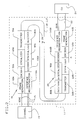
- a processor 12 such as a main frame IBM (Registered Trade Mark) Model 3090-200E processing system, is connected to one or more channels 14 for communication with peripheral devices 30, 32, 34 etc.
- the channel 14 communicates with device controllers 24, 26, 28, etc. across a standard channel to control unit interface which is fully described in a publication available from International Business Machines Corporation, entitled “IBM System/360 and System/370 I/O Interface Channel to Control Unit Original Equipment Manufacturers Information", publication number GA22-6974-08.
- This interface has been discussed in many prior art references including the Lynch and Thorn IBM Technical Disclosure Bulletin (TDB) article in the January, 1977 issue of the TDB and US-A-4,712,176, both discussed above.
- TDB Technical Disclosure Bulletin
- the standard System/370 channel interface thus described is a parallel interface which includes a number of control lines sometimes referred to as Tags such as SERVICE OUT, DATA OUT, ADDRESS OUT, COMMAND OUT, OP OUT, HOLD OUT, SELECT OUT, SUPPRESS OUT, SERVICE IN, DATA IN, ADDRESS IN, STATUS IN, OP IN, REQUEST IN, DISCONNECT IN and SELECT IN.
- Bus Out for transmission of data from channel to controller
- Bus In for transmission of data from controller to channel.
- Channel 14 communicates with controllers 24, 26, 28, etc. across the standard channel to controller interface discussed above on lines 15, 22, wherein lines 15 represent the channel to controller interface at the channel 14 end and lines 22 represent the channel to controller interfaces at the controller end.
- a serial data link adapter 17 connects the interface on lines 15 at one location to the interfaces on lines 22 at another location to extend the maximum distance that controllers and devices can be placed away from processors and channels.
- Serial data link adapter 17 includes two sub-adapters, 16 at the channel end and 20 at the controller end. The sub-adapters are connected by a serial link, such as an optical fibre duplex path 18.
- Sub-adapter 16 is also referred herein to as sub-adapter A and sub-adapter 20 is also referred to herein as sub-adapter B.
- serial data link adapter 17 including sub-adapters 16 and 20 will be described in greater detail.
- sub-adapters 16 and 20 are substantially the same, as can be seen from the diagram of Fig. 2.
- the data flow in sub-adapter 16 is from the channel to the serial data link 18 through the link 18 on lines 18 OUT indicating OUT bound data transmission and through the receive portion of sub-adapter 20 to the interface on lines 22 at the controller end.
- the data flow on the IN bound lines is from the parallel interface on lines 22 at the controller end through the transmit portion of sub-adapter 20 along data link IN bound path 18 IN and through the receive portion of sub-adapter 16 to the channel interface on lines 15.
- each sub-adapter having a transmit portion and a receive portion, for duplex operation, the sub-adapters will be described in such a way that common functions in the sub-adapters will be identified with common numeric reference characters having an alphabetic character A to represent the function in sub-adapter 16 and an alphabetic character B to represent the corresponding function in sub-adapter 20.
- the multi-character frame is then encoded by encoder 50A, 50B which may be efficiently implemented by the encoder and DC balanced 8/10 transmission code described in US-A-4,486,739.
- the encoded frame is then serialized by serializers 60A, 60B which may be implemented in any one of a number of well known parallel to serial converters.
- the serial multi-character frame is then converted from electrical signals to optical signals for transmission into the optical data link 18 by transmitters 70A, 70B and then transmitted from the optical data link 18 to the receiver 80A, 80B in the other sub-adapter 20, 16.
- Receivers 80A, 80B convert the optical signals to electrical signals for presentation to deserializer 90A, 90B which as with the serializers may be in a form of a well known serial to parallel converter which will not be further described herein.
- the received data in parallel form is then decoded by decoders 100A, 100B which decoders would be the compliment of the encoder described in US-A-4,486,739.
- the decoded frame is then operated on by interface reconstruction logic 110A, 110B where it is converted back to the protocol of the channel to controller interface. The logic for the interface reconstruction will be described in greater detail with respect to Fig. 4 below.
- the IN bound data path of serial data link adapter is substantially the mirror image of the OUT bound data path just described. Signals and data appear on the standard interface lines 22 from control units 24, etc. and are transmitted to frame generation logic 40B which is essentially the same as frame generation logic 40A discussed above with respect to sub-adapter 16.
- the multi-character frame information is then passed to encoder 50B for encoding in an appropriate run length code such as the eight/ten code described in US-A-4,486,739.
- the encoded frame is then serialized by serializers 60B and converted to optical signals and transmitted to sub-adapter 16 by a transmitter 70B over IN bound serial data link 18 IN.
- the IN bound portion of subadapter 16 includes a receiver 80A which performs the same function as receiver 80B in sub-adapter 20, a deserializer 90A, a decoder 110A and interface reconstruction logic 110A which perform the same functions as the corresponding functions 90B, 100B, 110B in sub-adapter 20.
- optical elements including transmitter 70A, 70B, and receivers 80A, 80B will not be further described since these elements are commercially available from a number of sources such as an American Telephone and Canal model ODL 200 transmit/receive pair.
- encoders 50A, 50B and decoders 100A, 100B will not be further described herein.
- the encoding scheme using the 8/10 DC balanced code as shown in US-A-4,486,739 incorporated herein will be employed. It should be noted that although the incorporated patent discloses a coding scheme and an encoder, it is easily within the skill of those skilled in the art to implement a decoder by reversing the functions of the encoder shown in Figs. 1 and following the incorporated patent.
- US-A-4,486,739 recognizes and identifies special characteristics for twelve characters identified with the first element K, and from these special K characters the error immunity characteristics of the arrangement being described are derived.
- Serializers and deserializers 60A and 60B and 90A, 90B may be implemented by any of a wide variety of serial to parallel and parallel to serial converters all of which are well-known in the art and do not require invention for implementation.
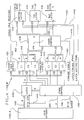
- the frame generation logic 40A, 40B will be described now in greater detail with reference to Fig. 3.
- the standard INPUT/OUTPUT interface on lines 15/22 includes a group of control or tag signals on lines 152 and a data bus on lines 151. These tag and bus lines are latched in multi-bit latches 154. Also, the tag lines are connected to a tag change detector 156 which examines tag signals for rising or falling edges indicating a change in tag condition. Tag change detector 156 controls transmit character control 158 which in turn controls gating of bus and tag latches 154 and buffer latches 160 and 162 as well as multiplexer 164 and encoder 50A, 50B. Both of the buffer latches 160 and 162 permit the loading of one frame into a latch such as buffer latch 160 while a previous frame which had been stored in buffer latch 162 is being transmitted.
- Buffer latches 160 and 162 can also be used for redundant frame transmission by storing a frame into one set of buffer latches 160 or 162 and transmitting the same frame twice to ensure error-free data transmission.
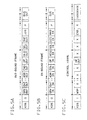
- the OUT bound frame shown in Fig. 5A includes a first character which has five bits dedicated to one of the twelve special K characters set forth in US-A-4,486,739 in Table 3. The next three bits of the first eight bit character provide the second half of the K character definition to determine whether the character is an idle character, an error idle character or one of several possible start characters. As seen in Fig. 3, the idle character defined as K28.5 is prestored in latches 166 and the error idle character defined as K29.7 is stored in latches 168.
- Each of these characters present eight bits on one set of inputs to a multiplexer 164 for selection for transmission under the control of transmit character control 158.
- the transmit character control block 158 causes the multiplexer 164 to select a combination of error idle characters from latches 168 with idle characters from latches 166 in sequence, for example a three character error idle sequence there might be one error idle character sent followed by two idle characters.
- transmit character control 158 would first gate the error idle character K29.7 from latches 168 through multiplexer 164 to encoder 50A, 50B followed by the idle character K28.5 from latches 166 through multiplexer 164 to encoder 50A, 50B twice in succession to form the three character frame idle error sequence.
- transmit character control 158 may be implemented by a simple State Machine with sequence control being triggered by a transmit byte clock on line 176 from encoder 50A, 50B.
- the SERVICE OUT tag and the DATA OUT tag occupy the last two bits of the first character of OUT bound frame and correspondingly the SERVICE IN and DATA IN tags occupy the last two bits of the first character of the IN bound frame as shown in Fig. 5B. Since there is a potential conflict between the start character and the service and DATA IN/OUT tags in the first character of the OUT bound frame and IN bound frame respectively, one of four different characters, K28.0, K28.2, K28.4, K28.6 must be selected as the start character depending on whether the SERVICE or DATA OUT/IN tags are active on the interface. For example, if the SERVICE OUT or DATE OUT tags are inactive, it is most likely that start character K28.0 will be used.
- the second character of both the OUT bound frame and the IN bound frame carry OUT tag lines and IN tags respectively, with the third character of both frames containing the eight bit BUS OUT on the OUT bound frame and BUS IN on the IN bound frame respectively.
- Interface reconstruction logic 110A and 110B performs this reconstruction function and may be readily implemented by the logic to be described as follows with reference to Fig. 4.
- decoder 100A, 100B As parallel characters are recovered and decoded by decoder 100A, 100B the K character as described above with reference to Figs. 5A and 5B is transmitted to frame control 402 on lines 404. If an error occurs in the encoder/decoder 50A, 50B, 100A, 100B, a coding error signal is presented on line 406 to frame control 402. Also, as a character is decoded, the eight bits of the character are presented to data latches 408 on eight bit bus 410 and a byte clock is presented on line 412 to latches 408 and frame control 402.
- each eight bit character is recovered, after it has been stored in latches 408, under the control of frame control 402, the characters are gated to the appropriate set of character latches 414 for the first character of a frame C1, 416 for the second character of a frame C2, 418 for the third character of a frame C3.
- a second frame would be stored, character by character, in character latches 420 for the first character C1, 422 for the second character C2, and 424 for the third character C3, respectively.
- One mode uses the transmission of a succession of single frames on the serial data link, each frame being followed by at least one idle character (K28.5) between frames.
- the second mode uses the transmission of a succession of double frames, each data frame being transmitted twice in succession with no idle characters being transmitted between the two identical frames.
- the transmit character control block 158 in the frame generation logic as 40A, 40B receives a signal identifying double frame transmission mode, which signal is used to set a 2 frame mode latch for controlling the gating of the nineteen bits stored in either buffer latches 160 or buffer latches 162 to the multiplexer 164.
- the nineteen bits from the selected latches 160 or 162 respectively will be gated twice on successive cycles to multiplexer 164 for encoding, serialization and transmission.
- the next frame stored in the other latches 162 or 160 respectively may then be sent twice in succession and so on.
- frame compare 426 compares the twenty four recovered bits of the first frame stored in latches 414, 416, and 418 respectively with the twenty four bits for the second frame stored in character latches 420, 422 and 424 respectively.
- Frame compare 426 operates under the control of frame control 402 when the compare enable line 428 is active. Compare enable is only active when the double frame transmission mode is being used. If there is a TRUE frame compare, compare output 430 provides enable signals to output latches 432 for control bits, 434, for tag lines and 436 for the data bus.
- the twenty-four bits of the frame are the output from latches 414, 416 and 418 on bus 438 which provides a first set of inputs to frame compare 426 and are connected to appropriate ones of control latches 432, tag latches 434 and data bus latches 436 respectively.
- a WRAP function is implemented using a control frame, such as the control frame shown in Fig. 5C.
- Serial data link sub-adapters 16 and 20 may have a wrap test button on a control panel. When the wrap test button is pressed, in either of the sub-adapters 16 or 20, a control frame is generated. The wrap bit (indicated as WRP in the first character of the control frame) is set to a predetermined state, and the serial data link between sub-adapters 16 and 20 is tested.
- the control frame is also used to test the integrity of the serial data link before it is enabled. To put a link into service, the serial data path must be attached, sub-adapter 16 and 20 must be powered up and sub-adapter 20 enabled. If these conditions are met, sub-adapter 16 can be enabled. Switching the link enable switch to the link enabled position generates a control frame with enable bit (ENB) as indicated in character 2 of control frame of Fig. 5C, set ON. Receipt of the return control frame from sub-adapter 20 verifies the integrity of the link and allows the link to be logically enabled. A control frame with the enable bit set ON forces sub-adapter 20 to perform a system reset to all remote control units and then sets the OP OUT tag to the state latched in the control frame.
- ENB enable bit
- a control frame is recognized by having a start character of K28.1 or K28.3.
- frame control 402 If a control frame has been decoded, frame control 402 generates a control frame enable signal on lines 442 to control latches 432 indicating that the information contained on bus 438 is control information and not tag or data information.
- the control information is used by the controllers 24, 26, 28, etc., for test and maintenance purposes and does not relate to the transmission of tag and data signals from channel to peripheral device.
- character K29.7 is established as the error idle character.
- An error idle sequence will consist of the error idle character K29.7 followed by two idle characters 28.5, thus the sequence will be K29.7, K28.5, K28.5. This sequence will be repeated on the line until corrected.
- An error idle detect circuit 450 is also connected to the eight bit parallel output of latches 408. If the eight bits presented at the output of latches 408 are the character K29.7 which represents the error idle condition, the error idle received signal is active on line 452, the output of error idle detect circuit 450.
- serial adapter 17 Each of the elements of serial adapter 17 has now been described.
- the information handling system having serial channel to control unit link as described above provides data communication with error immunity between elements of the information handling system without the need for cyclical redundancy checking (CRC) logic to be employed at either the transmitting or receiving end which eliminates the complexity of such CRC logic and reduces the number of bits which must be transmitted on the serial link.
- CRC cyclical redundancy checking
Landscapes
- Engineering & Computer Science (AREA)
- Theoretical Computer Science (AREA)
- Physics & Mathematics (AREA)
- General Engineering & Computer Science (AREA)
- General Physics & Mathematics (AREA)
- Communication Control (AREA)
- Detection And Prevention Of Errors In Transmission (AREA)
- Detection And Correction Of Errors (AREA)
Claims (10)
- Appareil pour transmettre des donnes entre un processeur (12) et un ou plusieurs dispositifs périphériques éloignés (30, 32, 34) comprenantun ou plusieurs canal (14) connecté entre ledit processeur et une ou plusieurs commande (24, 26, 28) de dispositif périphérique pour commander un ou plusieurs dispositif périphérique (30, 32, 34), en réponse aux signaux provenant dudit canal, conformément à un protocole de communication prédéterminé, etun adaptateur pour liaison de transmission de données en série (17) connecté entre l'un desdits canaux et une ou plusieurs desdites commandes de dispositif périphérique pour accroître l'étendue des communication entre lesdits canaux et les dites commandes,où
ledit adaptateur pour liaison de transmission de données en série (17) comprend un premier et un deuxième sous-adaptateurs (16, 20), chacun communicant avec l'autre par ladite liaison de transmission de données en série et chaque sous-adaptateur ayant des sections de transmission et de réception,
où ladite section de transmission de chacun desdits sous-adaptateurs comprendun moyen de création de trame (40A, 40B) qui répond aux signaux reçus respectivement dudit canal (14) et desdites commandes de dispositif périphériques, lesdits signaux se conformant audit protocole prédéterminé, ledit moyen de création de trame comprenant un moyen pour générer un ou plusieurs caractères d'une trame de départ unique en réponse aux signaux de commande reçus par ledit moyen de création de trame,un moyen pour créer des caractères libres prédéterminés, lesdits caractères libres ayant une relation immune aux erreurs avec lesdits caractères de trame de départ, de sorte que les caractères libres ayant des erreurs de bit simples et doubles qui sont transmis sur ladite liaison de transmission de données en série ne seront pas reconnus comme étant des caractères de départ de trame,un codeur (50A, 50B) pour coder les données pour une transmission efficace et sans erreur sur ladite liaison de transmission de données,un convertisseur parallèle-série (60A, 60B) pour convertir lesdites données codées, dudit format parallèle audit format série etune interface de liaison et un moyen d'excitation (110A, 110B) pour transmettre les données codées en série sur ladite liaison de transmission de données en série,et où ladite section de réception de chacun desdits sous-adaptateurs comprendun récepteur (80A, 80B) pour recevoir lesdites données en série codées;un convertisseur série-parallèle (90A, 90B) pour convertir lesdites données en série codées sous le format parallèle;un décodeur (100A, 100B) pour retrouver les données numériques sous une forme sans erreur; etun moyen d'interface (110A, 110B) pour reconstruire les données et les signaux de commande suivant ledit protocole prédéterminé pour les transmettre à ladite (ou auxdites) commande(s) de dispositif(s) périphérique(s) ou audit canal. - Appareil selon la revendication 1 dans lequel ledit moyen de création d'une trame comprend en outre un moyen de commande (158) pour commander la transmission de trames d'information sur ladite liaison de transmission de données en série dans un mode parmi une pluralité de modes de transmission prédéterminés.
- Appareil selon la revendication 2 dans lequel ledit moyen de commande (158) comprend un moyen pour commander la transmission de trames d'information dans un mode de double transmission sans l'intervention de caractères libre.
- Appareil selon la revendication 2 dans lequel ledit moyen de commande (158) comprend un moyen pour commander la transmission de trames d'information dans un mode de transmission à trame unique avec un ou plusieurs caractères libres intervenant entre les trames.
- Appareil selon la revendication 1 dans lequel ledit moyen de création de trame comprend en outre un moyen de commande (158) pour transmettre des signaux de commande et de données entre ledit canal et ladite commande de dispositif périphérique dans une trame unique contenant une pluralité de caractères.
- Appareil selon la revendication 5 où ladite trame comprend trois caractères,un premier caractère comprenant un caractère parmi une pluralité de caractères de départ prédéterminés, ledit caractère de départ étant choisi pour l'immunité aux erreurs en fonction d'un caractère libre,un deuxième caractère de ladite trame comprenant une pluralité de signaux de commande, etun troisième caractère de ladite trame comprenant une pluralité de signaux de données.
- Appareil selon la revendication 1 dans lequel ledit moyen d'interface pour la reconstruction comprend un moyen de commande pour trame pour commander la récupération de l'information sur trame transmise suivant l'un quelconque de ladite pluralité des modes de transmission.
- Appareil selon la revendication 7 dans lequel ledit moyen de commande pour trame comprend en outre un moyen pour détecter une trame de commande contenant des signaux utilisés pour tester l'intégrité dudit adaptateur de liaison pour la transmission de données en série.
- Appareil selon la revendication 1 dans lequel ledit moyen d'interface pour la reconstruction comprend en outre un moyen de comparaison des trames pour comparer une première et une deuxième transmission de trames transmises dans un mode de transmission à double trames pour tester l'intégralité de la transmission.
- Appareil selon la revendication 1 dans lequel ledit moyen d'interface pour la reconstruction comprend en outre un moyen pour détecter une séquence prédéterminée de caractères erronés, et un moyen pour transmettre ladite séquence de caractères erronés jusqu'à ce que ladite erreur ait été éliminée.
Applications Claiming Priority (2)
| Application Number | Priority Date | Filing Date | Title |
|---|---|---|---|
| US222679 | 1988-07-21 | ||
| US07/222,679 US4939735A (en) | 1988-07-21 | 1988-07-21 | Information handling system having serial channel to control unit link |
Publications (3)
| Publication Number | Publication Date |
|---|---|
| EP0352028A2 EP0352028A2 (fr) | 1990-01-24 |
| EP0352028A3 EP0352028A3 (fr) | 1991-07-17 |
| EP0352028B1 true EP0352028B1 (fr) | 1997-10-15 |
Family
ID=22833236
Family Applications (1)
| Application Number | Title | Priority Date | Filing Date |
|---|---|---|---|
| EP89307143A Expired - Lifetime EP0352028B1 (fr) | 1988-07-21 | 1989-07-14 | Appareil pour le transmission de données entre un processeur central et des dispositifs périphériques éloignés |
Country Status (4)
| Country | Link |
|---|---|
| US (1) | US4939735A (fr) |
| EP (1) | EP0352028B1 (fr) |
| JP (1) | JPH0720096B2 (fr) |
| DE (1) | DE68928381T2 (fr) |
Families Citing this family (35)
| Publication number | Priority date | Publication date | Assignee | Title |
|---|---|---|---|---|
| US5333271A (en) * | 1989-04-28 | 1994-07-26 | International Business Machines Corporation | Methods and apparatus for performing data chaining in data streaming mode through a channel extender |
| EP0412268B1 (fr) * | 1989-08-11 | 1996-09-11 | International Business Machines Corporation | Appareil pour l'interconnexion d'une unité de commande à bus parallèle avec un canal à liaison sérielle |
| EP0412269A3 (en) * | 1989-08-11 | 1992-02-26 | International Business Machines Corporation | Channel and extender unit operable with byte mode or non-byte mode control units |
| US5206946A (en) * | 1989-10-27 | 1993-04-27 | Sand Technology Systems Development, Inc. | Apparatus using converters, multiplexer and two latches to convert SCSI data into serial data and vice versa |
| US5155845A (en) * | 1990-06-15 | 1992-10-13 | Storage Technology Corporation | Data storage system for providing redundant copies of data on different disk drives |
| US5151977A (en) * | 1990-08-31 | 1992-09-29 | International Business Machines Corp. | Managing a serial link in an input/output system which indicates link status by continuous sequences of characters between data frames |
| US5488653A (en) * | 1991-09-04 | 1996-01-30 | Comsat Corporation | Facsimile interface unit (FIU) enhanced capabilities negotiation |
| EP0542087A3 (fr) * | 1991-11-10 | 1997-12-29 | Hewlett-Packard Company | Méthode et appareil pour transmission en série efficace des signaux de commande dans un bus numérique |
| US5414814A (en) * | 1992-05-08 | 1995-05-09 | The United States Of America As Represented By The Secretary Of The Navy | I/O interface between VME bus and asynchronous serial data computer |
| US6157967A (en) * | 1992-12-17 | 2000-12-05 | Tandem Computer Incorporated | Method of data communication flow control in a data processing system using busy/ready commands |
| USH1507H (en) * | 1993-04-23 | 1995-12-05 | The United States Of America As Represented By The Secretary Of The Navy | Demand assigned multiple access (DAMA) device controller interface |
| US5396505A (en) * | 1993-07-06 | 1995-03-07 | Tandem Computers Incorporated | Programmable error-checking matrix for digital communication system |
| US5752216A (en) * | 1994-07-06 | 1998-05-12 | Dimensions International, Inc. | Non-intrusive data interface system for air traffic control |
| DE69629758T2 (de) * | 1995-06-07 | 2004-06-03 | Compaq Computer Corp., Houston | Verfahren und Vorrichtung für die Überwachung des Datenflusses in einem fehlertoleranten Multiprozessorsystem |
| US5907566A (en) * | 1997-05-29 | 1999-05-25 | 3Com Corporation | Continuous byte-stream encoder/decoder using frequency increase and cyclic redundancy check |
| US6345330B2 (en) * | 1998-05-01 | 2002-02-05 | Acqis Technology, Inc. | Communication channel and interface devices for bridging computer interface buses |
| US6321335B1 (en) | 1998-10-30 | 2001-11-20 | Acqis Technology, Inc. | Password protected modular computer method and device |
| US6718415B1 (en) | 1999-05-14 | 2004-04-06 | Acqis Technology, Inc. | Computer system and method including console housing multiple computer modules having independent processing units, mass storage devices, and graphics controllers |
| US6643777B1 (en) | 1999-05-14 | 2003-11-04 | Acquis Technology, Inc. | Data security method and device for computer modules |
| US7308686B1 (en) | 1999-12-22 | 2007-12-11 | Ubicom Inc. | Software input/output using hard real time threads |
| WO2001046827A1 (fr) * | 1999-12-22 | 2001-06-28 | Ubicom, Inc. | Systeme et procede de traitement multifiliere au niveau des instructions dans un processeur integre au moyen d'une commutation d'environnement de temps zero |
| US7120783B2 (en) * | 1999-12-22 | 2006-10-10 | Ubicom, Inc. | System and method for reading and writing a thread state in a multithreaded central processing unit |
| US7047396B1 (en) | 2000-06-22 | 2006-05-16 | Ubicom, Inc. | Fixed length memory to memory arithmetic and architecture for a communications embedded processor system |
| US7010612B1 (en) * | 2000-06-22 | 2006-03-07 | Ubicom, Inc. | Universal serializer/deserializer |
| US6760367B1 (en) * | 2000-09-26 | 2004-07-06 | Eni Technology, Inc. | Internal noise immune data communications scheme |
| US20030120791A1 (en) * | 2001-12-20 | 2003-06-26 | Weber David M. | Multi-thread, multi-speed, multi-mode interconnect protocol controller |
| US7395337B2 (en) * | 2002-08-29 | 2008-07-01 | International Business Machines Corporation | Method, system, and program for establishing and requesting status on a computational resource |
| US7822950B1 (en) | 2003-01-22 | 2010-10-26 | Ubicom, Inc. | Thread cancellation and recirculation in a computer processor for avoiding pipeline stalls |
| GB0328435D0 (en) * | 2003-12-08 | 2004-01-14 | Tdk Systems Europ Ltd | Bluetooth communications |
| US7480840B2 (en) * | 2004-10-12 | 2009-01-20 | International Business Machines Corporation | Apparatus, system, and method for facilitating port testing of a multi-port host adapter |
| US7602318B1 (en) * | 2006-08-07 | 2009-10-13 | Integrated Device Technology, Inc. | Method and apparatus for improved efficiency in protocols using character coding |
| US7990724B2 (en) | 2006-12-19 | 2011-08-02 | Juhasz Paul R | Mobile motherboard |
| WO2008137058A1 (fr) * | 2007-05-03 | 2008-11-13 | James Boomer | Procédé et circuit de capture de sérialisation/ désérialisation données de clavier et de régénération d'interface de clavier |
| US9262270B2 (en) * | 2012-12-28 | 2016-02-16 | Intel Corporation | Live error recovery |
| DE102018213106B4 (de) * | 2018-08-06 | 2023-04-06 | Zf Friedrichshafen Ag | Adaptiervorrichtung zur Adaption eines Deserializers eines Steuergeräts für automatisierte Fahrfunktionen an mehrere Serializerprotokolle und Leiterplatte und Fahrerassistenzsystem umfassend die Adaptiervorrichtung |
Family Cites Families (5)
| Publication number | Priority date | Publication date | Assignee | Title |
|---|---|---|---|---|
| US3344353A (en) * | 1963-12-24 | 1967-09-26 | Philco Ford Corp | Error free data transmission system |
| US4486739A (en) * | 1982-06-30 | 1984-12-04 | International Business Machines Corporation | Byte oriented DC balanced (0,4) 8B/10B partitioned block transmission code |
| US4712176A (en) * | 1985-02-11 | 1987-12-08 | International Business Machines Corp. | Serial channel interface with method and apparatus for handling data streaming and data interlocked modes of data transfer |
| JPH0816891B2 (ja) * | 1985-10-01 | 1996-02-21 | 株式会社日立製作所 | チヤネルシステム |
| FR2606239A1 (fr) * | 1986-10-30 | 1988-05-06 | Bull Sa | Procede et dispositif de transmission de donnees numeriques |
-
1988
- 1988-07-21 US US07/222,679 patent/US4939735A/en not_active Expired - Fee Related
-
1989
- 1989-07-14 EP EP89307143A patent/EP0352028B1/fr not_active Expired - Lifetime
- 1989-07-14 DE DE68928381T patent/DE68928381T2/de not_active Expired - Fee Related
- 1989-07-20 JP JP1186205A patent/JPH0720096B2/ja not_active Expired - Lifetime
Non-Patent Citations (1)
| Title |
|---|
| pages 3139 - 3143; K.R.LYNCH et al: "SERIAL CHANNEL TO I/O INTERFACE" * |
Also Published As
| Publication number | Publication date |
|---|---|
| EP0352028A2 (fr) | 1990-01-24 |
| JPH0720096B2 (ja) | 1995-03-06 |
| DE68928381T2 (de) | 1998-03-26 |
| US4939735A (en) | 1990-07-03 |
| EP0352028A3 (fr) | 1991-07-17 |
| JPH0273736A (ja) | 1990-03-13 |
| DE68928381D1 (de) | 1997-11-20 |
Similar Documents
| Publication | Publication Date | Title |
|---|---|---|
| EP0352028B1 (fr) | Appareil pour le transmission de données entre un processeur central et des dispositifs périphériques éloignés | |
| EP0196911B1 (fr) | Réseaux locaux | |
| CA1218436A (fr) | Appareil emetteur-recepteur de donnees | |
| US3866175A (en) | Data communication system between a central computer and a plurality of data terminals | |
| JPH0561667B2 (fr) | ||
| US5748684A (en) | Resynchronization of a synchronous serial interface | |
| US4451898A (en) | Asynchronous interface message transmission using source and receive devices | |
| US5097410A (en) | Multimode data system for transferring control and data information in an i/o subsystem | |
| JPH04505692A (ja) | ファイバ分配式のインターフェイスされた光ファイバリンクのためのエラー検出方法及び装置 | |
| US3539998A (en) | Communications system and remote scanner and control units | |
| US5912752A (en) | Method and apparatus for improving serial infrared asynchronous communication performance | |
| EP0425779B1 (fr) | Dispositif et procédé de transmission de commandes | |
| US4823305A (en) | Serial data direct memory access system | |
| US4979095A (en) | Apparatus and method for a data processing system interface having multiple bit protocol signals | |
| JPS59183559A (ja) | デイジタル伝送装置 | |
| US4095277A (en) | Method for communicating text commands and instructions using conventional coded text characters and a structure for decoding and presenting command and instruction signals | |
| US3719930A (en) | One-bit data transmission system | |
| JP3252229B2 (ja) | デジタル・データ送信システム | |
| US4542517A (en) | Digital serial interface with encode logic for transmission | |
| JPH0548017B2 (fr) | ||
| JPH04348638A (ja) | データ伝送方法 | |
| US4651329A (en) | Digital decode logic for converting successive binary zero pulses having opposite polarity to a stream of data pulses | |
| JPS5870339A (ja) | 多重デ−タバスにおける機能的アドレツシングの方法 | |
| Machen | FOR LONG LINE, MULTICRATE APPLICATIONS | |
| JPH01131932A (ja) | データ転送装置 |
Legal Events
| Date | Code | Title | Description |
|---|---|---|---|
| PUAI | Public reference made under article 153(3) epc to a published international application that has entered the european phase |
Free format text: ORIGINAL CODE: 0009012 |
|
| AK | Designated contracting states |
Kind code of ref document: A2 Designated state(s): DE FR GB |
|
| 17P | Request for examination filed |
Effective date: 19900512 |
|
| PUAL | Search report despatched |
Free format text: ORIGINAL CODE: 0009013 |
|
| AK | Designated contracting states |
Kind code of ref document: A3 Designated state(s): DE FR GB |
|
| 17Q | First examination report despatched |
Effective date: 19940617 |
|
| GRAG | Despatch of communication of intention to grant |
Free format text: ORIGINAL CODE: EPIDOS AGRA |
|
| GRAH | Despatch of communication of intention to grant a patent |
Free format text: ORIGINAL CODE: EPIDOS IGRA |
|
| GRAH | Despatch of communication of intention to grant a patent |
Free format text: ORIGINAL CODE: EPIDOS IGRA |
|
| GRAA | (expected) grant |
Free format text: ORIGINAL CODE: 0009210 |
|
| AK | Designated contracting states |
Kind code of ref document: B1 Designated state(s): DE FR GB |
|
| PG25 | Lapsed in a contracting state [announced via postgrant information from national office to epo] |
Ref country code: FR Free format text: LAPSE BECAUSE OF FAILURE TO SUBMIT A TRANSLATION OF THE DESCRIPTION OR TO PAY THE FEE WITHIN THE PRESCRIBED TIME-LIMIT Effective date: 19971015 |
|
| REF | Corresponds to: |
Ref document number: 68928381 Country of ref document: DE Date of ref document: 19971120 |
|
| EN | Fr: translation not filed | ||
| PLBE | No opposition filed within time limit |
Free format text: ORIGINAL CODE: 0009261 |
|
| STAA | Information on the status of an ep patent application or granted ep patent |
Free format text: STATUS: NO OPPOSITION FILED WITHIN TIME LIMIT |
|
| 26N | No opposition filed | ||
| PGFP | Annual fee paid to national office [announced via postgrant information from national office to epo] |
Ref country code: GB Payment date: 20010702 Year of fee payment: 13 |
|
| PGFP | Annual fee paid to national office [announced via postgrant information from national office to epo] |
Ref country code: DE Payment date: 20010723 Year of fee payment: 13 |
|
| REG | Reference to a national code |
Ref country code: GB Ref legal event code: IF02 |
|
| PG25 | Lapsed in a contracting state [announced via postgrant information from national office to epo] |
Ref country code: GB Free format text: LAPSE BECAUSE OF NON-PAYMENT OF DUE FEES Effective date: 20020714 |
|
| PG25 | Lapsed in a contracting state [announced via postgrant information from national office to epo] |
Ref country code: DE Free format text: LAPSE BECAUSE OF NON-PAYMENT OF DUE FEES Effective date: 20030201 |
|
| GBPC | Gb: european patent ceased through non-payment of renewal fee |
Effective date: 20020714 |