EP0352549B1 - Additionneur à sélection de retenue - Google Patents
Additionneur à sélection de retenue Download PDFInfo
- Publication number
- EP0352549B1 EP0352549B1 EP89112769A EP89112769A EP0352549B1 EP 0352549 B1 EP0352549 B1 EP 0352549B1 EP 89112769 A EP89112769 A EP 89112769A EP 89112769 A EP89112769 A EP 89112769A EP 0352549 B1 EP0352549 B1 EP 0352549B1
- Authority
- EP
- European Patent Office
- Prior art keywords
- field effect
- channel field
- gate
- input
- effect transistor
- Prior art date
- Legal status (The legal status is an assumption and is not a legal conclusion. Google has not performed a legal analysis and makes no representation as to the accuracy of the status listed.)
- Expired - Lifetime
Links
Images

Classifications
-
- G—PHYSICS
- G06—COMPUTING OR CALCULATING; COUNTING
- G06F—ELECTRIC DIGITAL DATA PROCESSING
- G06F7/00—Methods or arrangements for processing data by operating upon the order or content of the data handled
- G06F7/38—Methods or arrangements for performing computations using exclusively denominational number representation, e.g. using binary, ternary, decimal representation
- G06F7/48—Methods or arrangements for performing computations using exclusively denominational number representation, e.g. using binary, ternary, decimal representation using non-contact-making devices, e.g. tube, solid state device; using unspecified devices
- G06F7/50—Adding; Subtracting
- G06F7/505—Adding; Subtracting in bit-parallel fashion, i.e. having a different digit-handling circuit for each denomination
- G06F7/506—Adding; Subtracting in bit-parallel fashion, i.e. having a different digit-handling circuit for each denomination with simultaneous carry generation for, or propagation over, two or more stages
- G06F7/507—Adding; Subtracting in bit-parallel fashion, i.e. having a different digit-handling circuit for each denomination with simultaneous carry generation for, or propagation over, two or more stages using selection between two conditionally calculated carry or sum values
-
- G—PHYSICS
- G06—COMPUTING OR CALCULATING; COUNTING
- G06F—ELECTRIC DIGITAL DATA PROCESSING
- G06F2207/00—Indexing scheme relating to methods or arrangements for processing data by operating upon the order or content of the data handled
- G06F2207/38—Indexing scheme relating to groups G06F7/38 - G06F7/575
- G06F2207/3804—Details
- G06F2207/386—Special constructional features
- G06F2207/3876—Alternation of true and inverted stages
Definitions
- the invention relates to a carry select adder with adder cells divided into blocks according to the preamble of patent claim 1.
- Adders are required for a large number of digital logic circuits, for example digital filters, signal processors and microprocessors.
- the simplest principle for such an adder is the “ripple-carry” method, in which an emerging carry (carry) is serially transmitted from an adder cell for the least significant bit to an adder cell for the most significant bit.
- the transit time of the carry signal essentially determines the addition time.
- the “carry select” method the adder cells of an adder, which are assembled in blocks, contain double carry paths.
- One Carry path each is used for a fictitious input signal on the input side of "0" or "1" at the input of an adder cell.
- a so-called block carrier signal which is formed from the two individual carrier signals of the last stage of the preceding block and its block carrier signal, decides which of the carrier paths is to be selected in the further course.
- the individual carry signals in each block are independent of the carry signal of previous blocks.
- At least two different adder cells are required, namely an input adder cell at the beginning of the block and a normal adder cell, which can follow in any number.
- Higher order blocks in the carry select adder contain a larger number of variable inputs and sum outputs, such as lower order blocks.
- Every single adder cell in the blocks contains two variable inputs, two carry inputs and outputs, one block carry input and output and one sum output.
- the number of variable inputs and total outputs in each block should be chosen so that the runtime of an individual Carrysignal corresponds to the runtime sum of the blockcarry signals up to this block.
- the block carrier signal is formed in the first stage of a block from the two carrier signals of the last stage of the preceding block and its block carrier signal.
- each block In the input stage of each block, the individual carry signals are only dependent on the variable inputs and the carry inputs are permanently connected to a "low” or “high” level.
- the carry signals in a "carry select” adder run through each block in parallel in two carry paths, one carry path for accepting a carry signal of "0" at the input of the block and a second carry path for accepting a carry signal of "1" at the block input is implemented in all adder cells.
- the Carry signals in the adder cells are dependent in a wide variety of ways on the input signals at the variable inputs of the adder cells and on Carry signals at the carry inputs of the adder cells.
- the invention has for its object to provide an adder circuit according to the "carry select" principle, which has a high processing speed.
- the advantage that can be achieved with the invention consists in particular in a simple construction of the adder circuit consisting of three different adder cells.
- Claims 2 to 5 are directed to a further embodiment of the invention.
- FIG. 1 shows a "carry select" adder block with adder cells B0, B1, B2, ... Bn, the adder cells B0, B1, B2 representing the first three adder cells of a block.
- any number of adder blocks are connected in series, the number of adder cells which are combined to form a block increasing with increasing order of the adder blocks.
- Each of the adder cells contains two variable inputs a0, b0; a1, b1; a2, b2, ... a n , b n , a block carry input BL 0e ; BL 1e ; BL 2e , ...
- BL ne a block carry output BL 0a ; BL 1a ; BL 2a , ... BL na , a sum output S0; S1; S2; ... S n , first and second carry inputs C0 0e , C1 0e ; C0 1e , C1 1e ; C0 2e , C1 2e ; .., C0 no , C1 no and first and second carry outputs C0 0a , C1 0a ; C0 1a , C1 1a ; C0 2a , C1 2a , ..., C0 na , C1 na .
- Each block consists of an input adder cell B0 as well as adder cells of a first and second type, the adder cells of the first and second type being alternately interconnected in a block.
- the first and second carry inputs C0 0e , C1 0e and the block carry input BL 0e of the input adder cell B0 of the first block are set for an addition to a fixed "low" level "0" in order to set fixed initial conditions for the addition process in the "carry select" -Add adders.
- the first and second inverted carry outputs C0 0a , C1 0a is an input adder cell B0 with the first and second inverted carry inputs, respectively C0 1e , C1 1e an adder cell of the first type B1 and the first and second non-inverted carry outputs C0 1a , C1 1a of the adder cells of the first type are connected to the first and second non-inverted carry inputs C0 2e , C1 2e of an adder cell of the second type B2, the block carry output BL 0a of the input adder cell B0 is also connected to the block carry input BL 1e of the adder cell of the first type B1 and the block carry output BL 1a of the adder cell of the first type B1 is connected to the block carry input BL 2e of the adder cell of the second type B2.
- the remaining adder cells within a block are alternately of the first type and the second type and are connected to one another analogously with their carry inputs and outputs and with their block carry inputs and outputs.
- the last adder cell Bn is of the first type and forms the end of a block for the "carry select" adder and contains the two inverted carry inputs in addition to the variable inputs a n , b n and the sum output S n C0 no , C1 no , the two non-inverted carry outputs C0 na , C1 na the block carry input and output BL ne , BL na .
- the block carrier signal for the adder block is formed in the input adder cell B0 and passed through the remaining adder cells of the adder block.
- the block carrier signal and the carrier signals of the previous adder block are evaluated to form a new block carrier signal.
- the carry signals of the input adder cell B0 of an adder block, which in the first and second inverted carry output C0 0a and C1 0a passed into the next adder cell of the first type B1 depend only on the variables at the variable inputs a0, b0 and not on the carrier signals at the first and second carry inputs C0 0e , C1 0e .
- the carry signals are additionally at the inverted or non-inverted carry inputs C0 1e , C1 1e or C0 2e , C1 2e for the carry signals at the non-inverted or inverted carry outputs C0 1a , C1 1a or C0 2a , C1 2a to consider.
- the alternating arrangement of adder cells of the first and second type B1, B2 according to FIG. 1 serves to accelerate the carry signals in the carry threads of the individual adder cells and thus to increase the processing speed of the "carry select" adder.
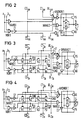
- FIG. 2 shows the block diagram of an input adder cell as it is present in the "carry select" adder at the beginning of each block.
- the input adder cell contains two NAND gates NAND 1, NAND2, five inverters I1, I3, I4, I5 and I6, a NOR gate NOR1, an ANDNOR gate ANDNOR1, two p-channel field effect transistors P5, P6, and n Channel field effect transistors N5 and N6.
- the first variable input a0 is connected to a first input of the first NAND gate NAND1 and to a first input of a NOR gate NOR1 and the second variable input b0 is connected to a second input of the first NAND gate NAND1 and to a second input of the NOR- Gate NOR1 interconnected.
- the output of the first NAND gate NAND1 forms the first inverted carry output C0 0a and is simultaneously connected to the first input of the second NAND gate NAND2 while the output of NOR gate NOR1 the second inverted carry output C1 0a represents and is connected via a first inverter I1 to the second terminal of the second NAND gate NAND2.
- the first carry input C 0e is connected to the NOR input of the ANDNOR gate ANDNOR1 and the second carry input C1 0e and the block carry input BL 0e are each connected to an AND input of the ANDNOR gate ANDNOR1, the output of the ANDNOR gate ANDNOR1 is over a second inverter I6 the block carry output BL 0a of the input adder cell.
- the output of the ANDNOR gate ANDNOR1 is via a third inverter I5 with the gate of a first p-channel field effect transistor P6 and the gate of a first n-channel field effect transistor N6 and to a first connection of a second p-channel field effect transistor P5 and connected to a first terminal of a second n-channel field effect transistor N5.
- the output of the second NAND gate NAND2 is connected on the one hand to the gate of the second p-channel field effect transistor P5 and on the other hand to a first connection of the first p-channel field effect transistor P6 and via a fourth inverter I3 to the gate of the second n -Channel field-effect transistor N5 and connected to the first connection of the first n-channel field-effect transistor N6.
- the second connection of the first and second N-channel field effect transistors N6, N5 and the second connection of the first and second p-channel field effect transistors P6, P5 are connected together to an input of a fifth inverter I4, at whose output the sum output S0 of the input adder cell is arranged.
- Fig. 3 shows a block diagram of an adder cell of the first type, which has a gate arrangement for two variables for evaluating a first and second carry input signal, for sum formation and for carry formation, and in each case one variable input being provided for one of the two variables.
- the gate arrangement of the adder cell of the first type is formed such that the charging of the capacitance of the first and second non-inverted carry outputs C0 1a , C1 1a either via two field-effect transistors P1, N2 acting as pull-up or pull-down transistors for the first non-inverted Carry output C0 1a or P3, N4 for the second non-inverted carry output C1 1a or via two series connections for the first and second non-inverted carry output C0 1a , C1 1a , each with an inverter gate I1, I2 and a further transfer transistor N1, P2 for the first non-inverted carry output C0 1a or N3, P4 for the second non-inverted carry output C1 1a .
- the adder cell of the first type is partially constructed with the same components as the input adder cell according to FIG. 2, so that the same reference numerals are used in FIGS. 3 and 2.
- the adder cell of the first type consists of two NAND gates NAND1, NAND2, five inverters I1, I2, I3, I4, I7, a NOR gate NOR1, an ORNAND gate ORNAND1, six n-channel field effect transistors N1, N2, N3 , N4, N5, N6, and six p-channel field effect transistors P1, P2, P3, P4, P5, P6.
- the p-channel field-effect transistors P1, P3 are used as pull-up transistors, the n-channel field-effect transistors N2, N4 as pull-down transistors and the remaining field-effect transistors as transfer transistors.
- the first variable input a1 of the adder cell of the first type is connected to the first input of the first NAND gate NAND1 and to the first input of the NOR gate NOR1, and the second variable input b1 is to the second input of the first NAND gate NAND1 and connected to the second input of the NOR gate NOR1.
- the output of the first NAND gate NAND1 is connected via a first inverter I2 to the first terminal of a first n-channel transfer transistor N1 and to the first terminal of a second n-channel transfer transistor N3, the first inverter I2 and the first n Channel transfer transistor N1 and the second n-channel transfer transistor N3 and the first inverter I2 each form a series circuit, and the output of the first NAND gate NAND1 is additionally connected to a first input of a second NAND gate NAND2 and to a gate connection of the first and second pull-up transistors P1, P3 connected.
- the output of the NOR gate NOR1 is connected via a second inverter I1 to the first connection of a first and second p-channel transfer transistor P2, P4.
- the output of the second inverter I1 is connected to a second input of the second NAND gate NAND2.
- the output of the NOR gate NOR1 is connected to a gate connection of a first and a second pull-down transistor N2, N4.
- the first connection of the first and second pulldown transistors N2, N4 is connected to ground GND, while the first connection of the first and second pullup transistors P1, P3 is connected to the supply voltage V DD .
- the first inverted carry input C0 1e is connected to a gate connection of the first n-channel transfer transistor N1 and the first p-channel transfer transistor P2 and to an AND input of the ORNAND gate ORNAND1, while the second inverted carry input C1 1e with a gate connection of the second n-channel transfer transistor N3 and the second p-channel transfer transistor P4 as well as with the first OR input of the ORNAND gate ORNAND1.
- the third further provides that the first non-inverted carry output C0 1a with the second connection of the first n-channel transfer transistor N1, with the second connection of the first p-channel transfer transistor P2, is connected to the second connection of the first pull-up transistor P1 and to the second connection of the first pull-down transistor N2 and the second non-inverted carry output C1 1a is connected to a second connection of a second n-channel transfer transistor N3, to a second connection of the second p-channel transfer transistor P4, connected to a second connection of the second pull-up transistor P3 and to a second connection of the second pull-down transistor N4.
- the block carry input BL 1e simultaneously forms the block carry output BL 1a and is connected via a third inverter I7 to a second OR input of the ORNAND gate ORNAND1.
- the output of the ORNAND gate ORNAND1 is each with a gate connection of the third p-channel transfer transistor P6 and the third n-channel transfer transistor N6 and with a first connection of a fourth p-channel transfer transistor P5 and a first connection of a fourth n- Channel transfer transistor N5 connected and the output of the second NAND gate NAND2 is connected to a first terminal of the third p-channel transfer transistor P6 and via a fourth inverter I3 to a first connection of the third n-channel transfer transistor N6 and to a gate connection of the fourth n-channel transfer transistor N5.
- the output of the second NAND gate NAND2 is connected to the gate terminal of the fourth p-channel transfer transistor P5 and the sum output S1 is in each case connected to a second terminal of the third and fourth p-channel transfer transistors P6, P5 and each connected to a second terminal of the third and fourth n-channel transfer transistors N6, N5.
- FIG. 4 shows a block diagram of an adder cell of the second type, which also has a gate arrangement for two variables for evaluating a first and second carry input signal, for sum formation and for carry formation, and one variable input is provided for one of the two variables.
- the gate arrangement of the second type adder cell is formed such that the capacitance of the first and second inverted carry outputs are charged C0 2a , C1 2a either via two field-effect transistors P1, N2 acting as pull-up or pull-down transistors for the first inverting carry output C0 2a or P3, N4 for the second inverted carry output C1 2a or via two transfer transistors N1, P2 for the first inverted carry output C0 2a or N3, P4 for the second inverted carry output C1 2a , happens.
- the adder cell of the second type is also partially constructed with the same components as the input adder cell according to FIG. 2 or the adder cell of the first type according to FIG. 3, so that the same reference numerals are used in FIG. 4, FIG. 3 and FIG. 2.
- the adder cell of the second type consists of two NAND gates NAND1, NAND2, a NOR gate NOR1, an ANDNOR gate ANDNOR1, four inverters I1, I2, I3, I4, six n-channel field effect transistors N1, N2, N3, N4 , N5, N6 and six p-channel field effect transistors P1, P2, P3, P4, P5, P6.
- the p-channel field effect transistors P1, P3 are used as pull-up transistors
- the n-channel field effect transistors N2, N4 are used as pull-down transistors
- the remaining field-effect transistors are used as transfer transistors.
- the first variable input a2 is connected to the first input of a first NAND gate NAND1 and to the first input of the NOR gate NOR1, while the second variable input b2 to the second input of the first NAND gate NAND1 and the second input of the NOR gate NOR1 is connected.
- the output of the first NAND gate NAND1 is connected via a first inverter I2 to a gate connection of a first and a second pulldown transistor N2, N4, and the output of the first NAND gate NAND1 is also connected to a first connection of a first p-channel Transfer transistor P2 and a first connection of a second p-channel transfer transistor P4 and also connected to a first connection of the second NAND gate NAND2.
- the output of the NOR gate NOR1 is connected via a second inverter I1 to a respective gate connection of the first and second pull-up transistors P1, P3 and to a second input of the NAND gate NAND2, and the output of the NOR gate NOR1 is still on connected to a first terminal of the first and second n-channel transfer transistors N1, N3.
- the first connection of the first and second pull-up transistors P1, P3 is connected to the supply voltage V DD in the adder cell of the second type according to FIG. 4, and a first connection of the first and second pull-down transistors N2, N4 is connected to ground GND.
- the first non-inverted carry input C0 2e is in each case connected to the gate of the first p-channel transfer transistor P2, the first n-channel transfer transistor N1 and to an OR input of the ANDNOR gate ANDNOR1 and the second non-inverted carry input C1 2e connected to the gate terminal of the second p-channel transfer transistor P4 and the second n-channel transfer transistor N3 and to a first AND input of the ANDNOR gate ANDNOR1.
- the block carry input BL 2e simultaneously forms the block carry output BL 2a of the adder cell of the second type and is simultaneously connected to a second AND input of the ANDNOR gate ANDNOR1.
- the first inverted carry output C0 2a Is respectively with a second connection of the first p-channel transfer transistor P2, the first n-channel transfer transistor N1, the first pulldown transistor N2 and the first pullup transistor P1 and the second inverted carry output C1 2a is connected to the second connection of the second p-channel transfer transistor P4, the second n-channel transfer transistor N3, the second pull-down transistor N4 and the second pull-up transistor P3.
- the output of the ANDNOR gate ANDNOR1 is connected to the gate terminal of the third n-channel transfer transistor N6, to the gate terminal of the third p-channel transfer transistor P6 and to a first terminal of the fourth n-channel transfer transistor N5 and the fourth p- Channel transfer transistor P5 connected and the output of the second NAND gate NAND2 is connected to a first terminal of the third n-channel transfer transistor N6 and to the gate terminal of the fourth n-channel transfer transistor N5 and via a third inverter I3 to the gate terminal of the fourth p-channel transfer transistor P5 and connected to a first terminal of the third p-channel transfer transistor P6.
- the sum output S2 is connected via a fourth inverter I4 to a second connection of the third and fourth n-channel transfer transistor N6, N5 and to a second connection of the third and fourth p-channel transfer transistor P5, P6.
- the pull-up transistors P1, P3 or the pull-down transistors N2, N4 and the further transfer transistors N1, N3 or P2, P4 are not part of a combination gate within the gate arrangement, so that the Transfer transistors inserted in a time-critical transmission path are optimized so that they form a small capacitance for the previous stage, but still represent a low-resistance source-drain path.
- the input adder cell and the adder cell of the second type are largely constructed identically, but all transfer transistors or pull-up and pull-down transistors N1, N2, N3, N4, P1, P2, P3, P4 are omitted. Since the Carry signals at the non-inverted carry inputs C0 0e or C1 0e of the input adder cell are only required together with the block carry signal at block carry input BL 0e to determine the new block carry signal, the input adder cell does not require any transfer transistors and the carry signals at the inverted first and second carry outputs C0 0a , C0 0a are only determined by the variables at the variable inputs a0, b0.
- the transfer transistors P2, N1 and P4, N3 in the adder cells of the first and second type have functional functions, while the pull-up and pull-down transistors P1, P3 and N2, N4 for better transmission of the supply voltage V DD and Ground GND are determined on the first and second carry outputs.
- the ANDNOR gate ANDNOR1 in the input adder cell serves to determine a new block-carrier signal, while the block-carrier signal in the remaining adder cells of an adder block is merely passed on.
- variable input part consisting of a NAND gate NAND1 and NOR gate NOR1. Both in the input adder cell and in the other adder cells, the carry signals at the two carry inputs and the block signal at the block carry input are evaluated and via the ANDNOR gate ANDNOR1 or the ORNAND gate ORNAND1 in the respective sum output part with the sum of the variables at the variable inputs forwarded to the corresponding total output.
Landscapes
- Physics & Mathematics (AREA)
- General Physics & Mathematics (AREA)
- Engineering & Computer Science (AREA)
- Computational Mathematics (AREA)
- Mathematical Analysis (AREA)
- Pure & Applied Mathematics (AREA)
- Theoretical Computer Science (AREA)
- Computing Systems (AREA)
- Mathematical Optimization (AREA)
- General Engineering & Computer Science (AREA)
- Logic Circuits (AREA)
Claims (5)
- Additionneur à sélection de retenues comportant des cellules d'additionneur subdivisées en blocs, chaque cellule d'additionneur comprenant deux entrées (a₀,b₀; a₁,b₁; a₂,b₂, ... an, bn) de variables, une entrée de retenue de bloc (BLOe; BL1e; BL2e...BLne), une sortie de retenue de bloc (BLOa; BL1a; BL2a...BLna), une sortie de somme (S₀; S₁, S₂ ...Sn), des première et deuxième entrées de retenue (C00e; C10e;
C01e ;C11e ; C02e; C12e; ...C00n ;C1en ) et des première et deuxième sorties de retenue (C00a ;C10a ; C01a; C11a;C02a ;C12a ,...C0na, C1na) et chaque bloc comprenant une cellule d'additionneur d'entrée et un nombre déterminé de cellules d'additionneur d'un premier et d'un second type, la première et la deuxième entrée (C00e; C10e) de retenue et l'entrée (BL0e) de retenue de bloc de la cellule d'additionneur d'entrée du premier bloc représentant d'autres entrées de variables, caractérisé en ce que la première et la deuxième sorties inverseuses de retenue (C00a ,C10a ) d'une cellule d'additionneur d'entrée sont connectées respectivement à la première et à la deuxième entrée inverseuse de retenue (C01e ,C11e ) d'une cellule d'additionneur du premier type, et la première et la deuxième sortie non inverseuse de retenue (C01a, C11a) de la cellule d'additionneur du premier type sont connectées respectivement à la première et à la deuxième entrée non inverseuse de retenue (C02e, C12e) d'une cellule d'additionneur du deuxième type, la sortie (BL0a) de retenue de bloc de la cellule d'additionneur d'entrée est reliée à l'entrée (BL1e) de retenue de bloc de la cellule d'additionneur du premier type et la sortie (BL1a) de retenue de bloc de la cellule d'additionneur du premier type est reliée à l'entrée de retenue de bloc (BL2e) de la cellule d'additionneur du deuxième type, et les autres cellules d'additionneur dans un bloc en alternance du premier type et du deuxième types sont reliées également les unes aux autres par l'intermédiaire des entrées et sorties de retenue et des entrées et sorties de retenue de bloc, la cellule d'additionneur d'entrée et les cellules d'additionneur du premier et du deuxième types comportant un dispositif de portes pour deux variables destinées à l'exploitation d'un premier et d'un second signal d'entrée de retenue, à la formation d'une somme et à la formation d'une retenue et une entrée de variables étant prévue pour une des deux variables, le dispositif de portes de la cellule d'additionneur du premier type est formé de telle sorte que la charge de la capacité des première et deuxième sorties non inverseuses de retenue (C01a, C11a) s'effectue soit par l'intermédiaire de deux transistors (P1, P3; N2, N4) à effet de champ agissant comme transistors reliant aux tensions hautes ou reliant aux tensions basses, soit par l'intermédiaire de deux circuits séries pour les première et deuxième sorties non inverseuses de retenue (C01a, C11a), les circuits séries comprenant chacun une porte inverseuse (I1, I2) et un transistor (N1, P2; N3, P4) à effet de champ agissant en tant que transistor de transfert, le dispositif de porte de la cellule d'additionneur du deuxième type est formé de telle sorte que la charge de la capacité des première et deuxième sorties inverseuses de retenue (C02a ,C12a ) est formée soit par l'intermédiaire de deux transistors (P1, P3; N2, N4) à effet de champ agissant en tant que transistors reliant aux tensions hautes ou aux tensions basses, soit par l'intermédiaire de deux transistors (N1, P2; N3, P4) à effet de champ agissant en tant que transistors de transfert pour les première et deuxième sorties (C02a ,C12a ) inverseuses de retenue et les transistors à effet de champ (N1, N2, N3, N4, P1, P2, P3, P4) agissant en tant que transistors reliant aux hautes tensions ou aux basses tensions et en tant que transistors de transfert ne font pas partie d'une porte combinatoire à l'intérieur du dispositif de portes. - Additionneur à sélection de retenues suivant la revendication 1, caractérisé en ce que lors d'une addition de signaux d'entrée, qui sont appliqués aux entrées (a₀, b₀; a₁, b₁; a₂, b₂; ...an, bn) de variables de chaque cellule d'additionneur, les autres entrées de variables sont connectées à un niveau fixe bas.
- Additionneur à sélection de retenue suivant la revendication 1 ou 2, caractérisé en ce que la cellule d'additionneur d'entrées comprend deux portes NON-ET (NAND1, NAND2), cinq inverseurs (I1, I3, I5, I6), une porte NON-OU (NOR1), une porte ANDNOR (ANDNOR1), deux transistors (N5, N6) à effet de champ à canal n, deux transistros (P5,P6) à effet de champ à canal p, la première entrée (a₀) de variables est reliée à une première entrée d'une première porte NON-ET (NAND1) et à la première entrée d'une porte NON-OU (NOR1), la deuxième entrée (b₀) de variables est reliée à la deuxième entrée de la première porte NON-ET (NAND1) et à la deuxième entrée de la porte NON-OU (NOR1), la sortie de retenue de la première porte NON-ET (NAND1) forme la première sortie inverseuse de retenue (
C00a ) et est connectée en même temps à la première entrée de la deuxième porte NON-ET (NAND2), la sortie de retenue de la porte NON-OU (NOR1) forme la deuxième sortie (C11a ) inverseuse de retenue et est connectée par l'intermédiaire d'un premier inverseur (I1) à la deuxième borne de la deuxième porte NON-ET (NAND2), la première entrée (C00e) de retenue est connectée à l'entrée NOR de la porte ANDNOR (ANDNOR1) et la deuxième entrée de retenue (C10e) et l'entrée (BL0e) de retenue de bloc est connectée à une entrée AND de la porte ANDNOR (ANDNOR1), la sortie de la porte ANDNOR (ANDNOR1) forme, par l'intermédiaire d'un deuxième inverseur (I6) la sortie (BL0a) de retenue de bloc de la cellule d'additionneur d'entrée et la sortie de la porte ANDNOR (ANDNOR1) est connectée par l'intermédiaire d'un troisième inverseur (I5) à la grille d'un premier transistor (P6) à effet de champ à canal p et à la grille d'un premier transistor (N6) à effet de champ à canal n, ainsi qu'à une première borne d'un deuxième transistor (P5) à effet de champ à canal p et à une première borne d'un deuxième transistor (N5) à effet de champ à canal n, la sortie de la deuxième porte NON-ET (NAND2) est connectée d'une part à la grille du deuxième transistor (P5) à effet de champ à canal p et d'autre part à une première borne du premier transistor (P6) à effet de champ à canal p et est connectée par l'intermédiaire d'un quatrième inverseur (I3) à la grille du deuxième transistor (N5) à effet de champ à canal n et à la première borne du premier transistor (N6) à effet de champ à canal n, la deuxième borne des premier et deuxième transistors (N6,N5) à effet de champ à canal n et la deuxième borne des premier et deuxième transistors (P6, P5) à effet de champ à canal p sont connectées à l'entrée d'un cinquième inverseur (I4) et la sortie du cinquième inverseur (I4) forme la sortie (S₀) de somme de la cellule d'additionneur d'entrée. - Additionneur à sélection de retenues selon la revendication 1 ou 2, caractérisé en ce que la cellule d'additionneur du premier type comprend deux portes NON-ET (NAND1, NAND2), cinq inverseurs (I1, I2, I4, I7), une porte NON-OU (NOR1), une porte ORNAND (ORNAND1), six transistors à effet de champ à canal n (N1, N2, N3, N4, N5, N6) et six transistors à effet de champ à canal p (P1, P2, P3, P4, P5, P6), la première entrée (a₁) de variables de la cellule d'additionneur du premier type est reliée à la première entrée de la première porte NON-ET (NAND1) et à la première entrée de la porte NON-OU (NOR1), la deuxième entrée (b₁) de variables est connectée à la deuxième entrée de la première porte NON-ET (NAND1) et à la deuxième entrée de la porte NON-OU (NOR1), la sortie de la première porte NON-ET (NAND1) est reliée par l'intermédiaire d'un premier inverseur (I2) à la première borne d'un premier transistor (N1) à effet de champ à canal n et à la première borne d'un deuxième transistor (N3) à effet de champ à canal n, le premier inverseur (I2) et le premier transistor (N1) à effet de champ à canal n ainsi que le deuxième transistor (N3) à effet de champ à canal n et le premier inverseur (I2) formant un circuit série, la sortie de la première porte NON-ET (NAND1) est reliée à une première entrée d'une deuxième porte NON-ET (NAND2) et à chacune des bornes de grille d'un premier et d'un deuxième transistors (P1, P3) à effet de champ à canal p, chacune des premières bornes des premier et deuxième transistors (P1, P3) à effet de champ à canal p est connectée à la tension (VDD) d'alimentation, la sortie de la porte NON-OU (NOR1) est connectée par l'intermédiaire d'un deuxième inverseur (I1) à la première borne d'un troisième et d'un quatrième transistors (P2, P4) à effet de champ à canal p, la sortie du deuxième inverseur (I1) est reliée à la deuxième entrée de la deuxième porte NON-ET (NAND2), la sortie de la porte NON-OU (NOR1) est connectée à chacune des bornes de grille d'un troisième et d'un quatrième transistors (N2, N4) à effet de champ à canal n, une première borne des troisième et quatrième transistors (N2, N4) à effet de champ à canal n est reliée à la masse (GND), la première entrée (
C01e ) inverseuse de retenue est reliée à chacune des bornes de grille du premier transistor (N1) à effet de champ à canal n et du troisième transistor (P2) à effet de champ à canal p et à une entrée NAND de la porte ORNAND (ORNAND1), la deuxième entrée (C11e ) inverseuse de retenue est connectée à chacune des bornes de grille du deuxième transistor (N3) à effet de champ à canal n et du quatrième transistor (P4) à effet de champ à canal p ainsi qu'à une première entrée OR de la porte ORNAND (ORNAND1), la première sortie (C01a) non inverseuse de retenue est connectée à une deuxième borne du premier transistor (N1) à effet de champ à canal n, à une deuxième borne du premier transistor (P1) à effet de champ à canal p, à une deuxième borne du troisième transistor (P2) à effet de champ à canal p, et à une deuxième borne du troisième transistor (N2) à effet de champ à canal n, la deuxième sortie (C11a) non inverseuse de retenue est connectée à une deuxième borne du deuxième transistor (N3) à effet de champ à canal n, à une deuxième borne du deuxième transistor (P3) à effet de champ à canal p, à une deuxième borne du quatrième transistor (P4) à effet de champ à canal p, ainsi qu'à une deuxième borne du quatrième transistor (N4) à effet de champ à canal n, l'entrée (BL1e) de retenue de bloc forme la sortie (BL1a) de retenue de bloc et est connectée par l'intermédiaire d'un troisième inverseur (I7) à une deuxième entrée OR de la porte ORNAND (ORNAND1), la sortie de la porte ORNAND (ORNAND1) est reliée à chacune des bornes de grille d'un cinquième transistor (P6) à effet de champ à canal p et d'un cinquième transistor (N6) à effet de champ à canal n ainsi qu'à une première borne d'un sixième transistor (P5) à effet de champ à canal p et à une première borne d'un sixième transistor (N5) à effet de champ à canal n, la sortie de la deuxième porte NON-ET (NAND2) est reliée à une première borne du cinquième transistor (P6) à effet de champ à canal p et à la borne de grille du sixième transistor (P5) à effet de champ à canal p et par l'intermédiaire d'un quatrième inverseur (I3) à une première borne du cinquième transistor (N6) à effet de champ à canal n et à la borne de grille du sixième transistor (N5) à effet de champ à canal n, la sortie (S₁) de somme est reliée par l'intermédiaire d'un cinquième inverseur (I4) à chacune des deuxièmes bornes des cinquième et sixième transistors (P6, P5) à effet de champ à canal p et à chacune des deuxièmes bornes des cinquième et sixième transistors (N6, N5) à effet de champ à canal n. - Additionneur à sélection de retenues suivant la revendication 1 ou 2, caractérisé en ce que la cellule d'additionneur du deuxième type comprend deux portes NON-ET (NAND1, NAND2), une porte NON-OU (NOR1, NOR2), une porte ANDNOR (ANDNOR1), quatre inverseurs (I1,I2,I3,I4), six transistors (N1,N2,N3,N4,N5,N6) à effet de champ à canal n, six transistors (P1,P2,P3,P4,P5,P6) à effet de champ à canal p, la première entrée (a₂) de variables est reliée à la première entrée d'une première porte NON-ET (NAND1) et à la première entrée de la porte NON-OU (NOR1), la deuxième entrée (b₂) de variables est connectée à la deuxième entrée de la première porte NON-ET (NAND1) et la deuxième entrée de la porte NON-OU (NOR1), la sortie de la première porte NON-ET (NAND1) est connectée par l'intermédiaire d'un premier inverseur (I2) à chacune des bornes de grille d'un premier et d'un deuxième transistor (N2,N4) à effet de champ à canal n, la sortie de la première porte NON-ET (NAND1) est reliée à la fois à une première borne d'un premier transistor (P2) à effet de champ à canal p, à une première borne d'un deuxième transistor (P4) à effet de champ à canal p et aussi à une première borne de la deuxième porte NON-ET (NAND2), une première borne des premier et deuxième transistors (N2, N4) à effet de champ à canal n est reliée à la masse (GND), la sortie de la porte NON-OU (NOR1) est reliée par l'intermédiaire d'un deuxième inverseur (I1) à chacune des bornes de grille des troisième et quatrième transistors (P1, P3) à effet de champ à canal p et à une deuxième entrée de la porte NON-ET (NAND2), la sortie de la porte NON-OU (NOR1) est connectée à chacune des premières bornes de troisième et quatrième transistors (N1, N3) à effet de champ à canal n, chaque première borne des troisième et quatrième transistors (P1, P3) à effet de champ à canal p est reliée à la tension (VDD) d'alimentation, la première entrée (C02e) non inverseuse de retenue est connectée à chacune des bornes de grille du premier transistor (P2) à effet de champ à canal p et du troisième transistor (N1) à effet de champ à canal n ainsi qu'à une première entrée NOR de la porte ANDNOR (ANDNOR1) et la deuxième entrée non inverseuse (C12a) de retenue est connectée à chacune des bornes de grille du deuxième transistor (P4) à effet de champ à canal p et du quatrième transistor (N3) à effet de champ à canal n ainsi qu'à une première entrée AND de la porte ANDNOR (ANDNOR1), l'entrée (BL2e) de retenue de bloc est connectée à une deuxième entrée AND de la porte ANDNOR (ANDNOR1) et forme la sortie (BL2a) de retenue de bloc, la première sortie (
C02a ) inverseuse de retenue est reliée à chacune des deuxièmes bornes du premier transistor (P2) à effet de champ à canal p, du premier transistor (N2) à effet de champ à canal n, du troisième transistor (N1) à effet de champ à canal n et du troisième transistor (P1) à effet de champ à canal p, la deuxième sortie inverseuse (C11a ) de retenue est reliée à chacune des deuxièmes bornes du deuxième transistor (P4) à effet de champ à canal p, du deuxième transistor (N4) à effet de champ à canal n, du quatrième transistor (N3) à effet de champ à canal n, et du quatrième transistor (P3) à effet de champ à canal p, la sortie de la porte ANDNOR (ANDNOR1) est connectée à la borne de grille d'un cinquième transistor (N6) à effet de champ à canal n, à la borne de grille d'un cinquième transistor (P6) à effet de champ à canal p ainsi qu'à chacune des premières bornes d'un sixième transistor (N5) à effet de champ à canal n et d'un sixième transistor (P5) à effet de champ à canal p, la sortie de la deuxième porte NON-ET (NAND2) est reliée à une première borne du cinquième transistor (N6) à effet de champ à canal n et à la borne de grille du sixième transistor (N5) à effet de champ à canal n ainsi que par l'intermédiaire d'un troisième inverseur (I3) à la borne de grille du sixième transistor (P5) à effet de champ à canal p et à une première borne du cinquième transistor (P6) à effet de champ à canal p et la sortie (S2) de somme est connectée par l'intermédiaire d'un quatrième inverseur (I4) à chacune des deuxièmes bornes des cinquième et sixième transistors (N6, N5) à effet de champ à canal n et à chacune des deuxièmes bornes des cinquième et sixième transistors (P6, P5) à effet de champ à canal p.
Applications Claiming Priority (2)
| Application Number | Priority Date | Filing Date | Title |
|---|---|---|---|
| DE3825969 | 1988-07-29 | ||
| DE3825969 | 1988-07-29 |
Publications (3)
| Publication Number | Publication Date |
|---|---|
| EP0352549A2 EP0352549A2 (fr) | 1990-01-31 |
| EP0352549A3 EP0352549A3 (fr) | 1991-10-16 |
| EP0352549B1 true EP0352549B1 (fr) | 1995-06-07 |
Family
ID=6359926
Family Applications (1)
| Application Number | Title | Priority Date | Filing Date |
|---|---|---|---|
| EP89112769A Expired - Lifetime EP0352549B1 (fr) | 1988-07-29 | 1989-07-12 | Additionneur à sélection de retenue |
Country Status (4)
| Country | Link |
|---|---|
| US (1) | US5027312A (fr) |
| EP (1) | EP0352549B1 (fr) |
| JP (1) | JPH0275019A (fr) |
| DE (1) | DE58909280D1 (fr) |
Families Citing this family (11)
| Publication number | Priority date | Publication date | Assignee | Title |
|---|---|---|---|---|
| JP3214086B2 (ja) * | 1992-09-04 | 2001-10-02 | 株式会社日立製作所 | 桁上げ先見回路 |
| US5508952A (en) * | 1993-10-19 | 1996-04-16 | Kantabutra; Vitit | Carry-lookahead/carry-select binary adder |
| US5636157A (en) * | 1994-10-03 | 1997-06-03 | International Business Machines Corporation | Modular 64-bit integer adder |
| US5978826A (en) * | 1995-12-01 | 1999-11-02 | Lucent Techologies Inc. | Adder with even/odd 1-bit adder cells |
| US6003059A (en) * | 1997-02-21 | 1999-12-14 | International Business Machines Corp. | Carry select adder using two level selectors |
| US6438572B1 (en) | 1998-09-21 | 2002-08-20 | Rn2R, L.L.C. | Adder having reduced number of internal layers and method of operation thereof |
| US6259275B1 (en) | 2000-05-01 | 2001-07-10 | Rn2R, L.L.C. | Logic gate having reduced power dissipation and method of operation thereof |
| US7571204B1 (en) * | 2000-09-21 | 2009-08-04 | Stmicroelectronics, Inc. | M-bit race delay adder and method of operation |
| US6748411B1 (en) | 2000-11-20 | 2004-06-08 | Agere Systems Inc. | Hierarchical carry-select multiple-input split adder |
| JP4118587B2 (ja) * | 2002-04-09 | 2008-07-16 | サンデン株式会社 | 可変容量圧縮機 |
| DE102012103195A1 (de) * | 2012-04-13 | 2013-10-17 | Mwm Gmbh | Kolben einer Brennkraftmaschine |
Family Cites Families (10)
| Publication number | Priority date | Publication date | Assignee | Title |
|---|---|---|---|---|
| US3100835A (en) * | 1960-01-06 | 1963-08-13 | Ibm | Selecting adder |
| JPS5892036A (ja) * | 1981-11-27 | 1983-06-01 | Toshiba Corp | 加算回路 |
| GB2127187B (en) * | 1982-08-23 | 1986-03-05 | Hewlett Packard Co | Circuits for operating on n-digit operands |
| US4525797A (en) * | 1983-01-03 | 1985-06-25 | Motorola, Inc. | N-bit carry select adder circuit having only one full adder per bit |
| JPS6055438A (ja) * | 1983-09-05 | 1985-03-30 | Matsushita Electric Ind Co Ltd | 2入力加算器 |
| US4704701A (en) * | 1984-11-01 | 1987-11-03 | Raytheon Company | Conditional carry adder for a multibit digital computer |
| US4623982A (en) * | 1985-06-10 | 1986-11-18 | Hewlett-Packard Company | Conditional carry techniques for digital processors |
| EP0218071B1 (fr) * | 1985-09-30 | 1993-02-17 | Siemens Aktiengesellschaft | Cellule d'addition pour un additionneur à propagation de retenue en technique CMOS |
| FR2596544B1 (fr) * | 1986-03-28 | 1988-05-13 | Radiotechnique Compelec | Circuit arithmetique et logique |
| EP0257362A1 (fr) * | 1986-08-27 | 1988-03-02 | Siemens Aktiengesellschaft | Additionneur |
-
1989
- 1989-07-12 DE DE58909280T patent/DE58909280D1/de not_active Expired - Fee Related
- 1989-07-12 EP EP89112769A patent/EP0352549B1/fr not_active Expired - Lifetime
- 1989-07-17 US US07/380,601 patent/US5027312A/en not_active Expired - Fee Related
- 1989-07-25 JP JP1192471A patent/JPH0275019A/ja active Pending
Also Published As
| Publication number | Publication date |
|---|---|
| US5027312A (en) | 1991-06-25 |
| DE58909280D1 (de) | 1995-07-13 |
| EP0352549A3 (fr) | 1991-10-16 |
| EP0352549A2 (fr) | 1990-01-31 |
| JPH0275019A (ja) | 1990-03-14 |
Similar Documents
| Publication | Publication Date | Title |
|---|---|---|
| DE4212202C2 (de) | Logikgatter | |
| EP0583298B1 (fr) | Circuit logique pour circuits asynchrones avec un bloc logique a canal n et un bloc logique a canal p inverse du premier | |
| EP0633662B1 (fr) | Montage pour un oscillateur en anneau | |
| DE3940897C2 (de) | Schaltungsanordnung und Verfahren zur Berechnung digitaler Summen in einem Halbleiteraddierer mit Parallelübertrag | |
| DE2707451C2 (de) | Paralleladdierwerk mit durchlaufendem Übertrag zum Addieren von wenigstens zwei aus mehreren Bits bestehenden Summanden | |
| DE68927560T2 (de) | Hochgeschwindige, hochleistende Nulldetektorschaltung mit Parallelverarbeitung | |
| EP0178424B1 (fr) | Multiplieur numérique sémisystolique à structure cellulaire | |
| DE69430035T2 (de) | CMOS-Schaltung zum Ausführen von bollescher Funktionen | |
| EP0352549A2 (fr) | Additionneur à sélection de retenue | |
| EP0209014A2 (fr) | Dispositif ayant un additionneur à réservation de retenue saturable | |
| DE19826315A1 (de) | Binärer Komparator | |
| DE112005001906B4 (de) | Mehrbit-Addierer und Verfahren zum Propagieren, Generieren oder Killen von Carry-In-Bits entlang einer Carry-Kette | |
| EP0257362A1 (fr) | Additionneur | |
| DE69216669T2 (de) | Josephson Gatter mit einer Vielzahl von Eingangstoren und Josephson Schaltung mit solchem Gatter | |
| DE69328419T2 (de) | Trommelverschiebevorrichtung. | |
| EP0224656B1 (fr) | Additionneur à propagation de retenue à plusieurs étages en technique CMOS avec deux types de cellules d'addition | |
| DE10305849B3 (de) | Carry-Ripple Addierer | |
| DE69319481T2 (de) | Zeilendekodierer zum Antreiben einer Wortleitung in mehrernpunkten | |
| DE10227618B4 (de) | Logikschaltung | |
| EP0905892B1 (fr) | Bascule RS avec des entrées de validation | |
| DE2017132A1 (de) | Binarer Parallel Addierer | |
| EP0218071B1 (fr) | Cellule d'addition pour un additionneur à propagation de retenue en technique CMOS | |
| EP0333884B1 (fr) | Circuit multiplieur parallèle-série ainsi que ses étages de multiplication et d'addition | |
| DE68928370T2 (de) | Logikschaltung mit Uebertragungsgesteuerten Addierer | |
| DE4422784C2 (de) | Schaltungsanordnung mit wenigstens einer Schaltungseinheit wie einem Register, einer Speicherzelle, einer Speicheranordnung oder dergleichen |
Legal Events
| Date | Code | Title | Description |
|---|---|---|---|
| PUAI | Public reference made under article 153(3) epc to a published international application that has entered the european phase |
Free format text: ORIGINAL CODE: 0009012 |
|
| AK | Designated contracting states |
Kind code of ref document: A2 Designated state(s): DE FR GB |
|
| 17P | Request for examination filed |
Effective date: 19901205 |
|
| PUAL | Search report despatched |
Free format text: ORIGINAL CODE: 0009013 |
|
| AK | Designated contracting states |
Kind code of ref document: A3 Designated state(s): DE FR GB |
|
| 17Q | First examination report despatched |
Effective date: 19941006 |
|
| GRAA | (expected) grant |
Free format text: ORIGINAL CODE: 0009210 |
|
| AK | Designated contracting states |
Kind code of ref document: B1 Designated state(s): DE FR GB |
|
| REF | Corresponds to: |
Ref document number: 58909280 Country of ref document: DE Date of ref document: 19950713 |
|
| GBT | Gb: translation of ep patent filed (gb section 77(6)(a)/1977) |
Effective date: 19950821 |
|
| ET | Fr: translation filed | ||
| PLBE | No opposition filed within time limit |
Free format text: ORIGINAL CODE: 0009261 |
|
| STAA | Information on the status of an ep patent application or granted ep patent |
Free format text: STATUS: NO OPPOSITION FILED WITHIN TIME LIMIT |
|
| 26N | No opposition filed | ||
| PGFP | Annual fee paid to national office [announced via postgrant information from national office to epo] |
Ref country code: DE Payment date: 19960917 Year of fee payment: 8 |
|
| PGFP | Annual fee paid to national office [announced via postgrant information from national office to epo] |
Ref country code: GB Payment date: 19970620 Year of fee payment: 9 |
|
| PGFP | Annual fee paid to national office [announced via postgrant information from national office to epo] |
Ref country code: FR Payment date: 19970718 Year of fee payment: 9 |
|
| PG25 | Lapsed in a contracting state [announced via postgrant information from national office to epo] |
Ref country code: DE Free format text: LAPSE BECAUSE OF NON-PAYMENT OF DUE FEES Effective date: 19980401 |
|
| PG25 | Lapsed in a contracting state [announced via postgrant information from national office to epo] |
Ref country code: GB Free format text: LAPSE BECAUSE OF NON-PAYMENT OF DUE FEES Effective date: 19980712 |
|
| GBPC | Gb: european patent ceased through non-payment of renewal fee |
Effective date: 19980712 |
|
| PG25 | Lapsed in a contracting state [announced via postgrant information from national office to epo] |
Ref country code: FR Free format text: LAPSE BECAUSE OF NON-PAYMENT OF DUE FEES Effective date: 19990331 |
|
| REG | Reference to a national code |
Ref country code: FR Ref legal event code: ST |