EP0209014A2 - Dispositif ayant un additionneur à réservation de retenue saturable - Google Patents
Dispositif ayant un additionneur à réservation de retenue saturable Download PDFInfo
- Publication number
- EP0209014A2 EP0209014A2 EP86109135A EP86109135A EP0209014A2 EP 0209014 A2 EP0209014 A2 EP 0209014A2 EP 86109135 A EP86109135 A EP 86109135A EP 86109135 A EP86109135 A EP 86109135A EP 0209014 A2 EP0209014 A2 EP 0209014A2
- Authority
- EP
- European Patent Office
- Prior art keywords
- carry
- adders
- inputs
- bits
- subtotal
- Prior art date
- Legal status (The legal status is an assumption and is not a legal conclusion. Google has not performed a legal analysis and makes no representation as to the accuracy of the status listed.)
- Granted
Links
Images


Classifications
-
- G—PHYSICS
- G06—COMPUTING OR CALCULATING; COUNTING
- G06F—ELECTRIC DIGITAL DATA PROCESSING
- G06F7/00—Methods or arrangements for processing data by operating upon the order or content of the data handled
- G06F7/38—Methods or arrangements for performing computations using exclusively denominational number representation, e.g. using binary, ternary, decimal representation
- G06F7/48—Methods or arrangements for performing computations using exclusively denominational number representation, e.g. using binary, ternary, decimal representation using non-contact-making devices, e.g. tube, solid state device; using unspecified devices
- G06F7/50—Adding; Subtracting
- G06F7/505—Adding; Subtracting in bit-parallel fashion, i.e. having a different digit-handling circuit for each denomination
- G06F7/509—Adding; Subtracting in bit-parallel fashion, i.e. having a different digit-handling circuit for each denomination for multiple operands, e.g. digital integrators
- G06F7/5095—Adding; Subtracting in bit-parallel fashion, i.e. having a different digit-handling circuit for each denomination for multiple operands, e.g. digital integrators word-serial, i.e. with an accumulator-register
-
- G—PHYSICS
- G06—COMPUTING OR CALCULATING; COUNTING
- G06F—ELECTRIC DIGITAL DATA PROCESSING
- G06F7/00—Methods or arrangements for processing data by operating upon the order or content of the data handled
- G06F7/38—Methods or arrangements for performing computations using exclusively denominational number representation, e.g. using binary, ternary, decimal representation
- G06F7/48—Methods or arrangements for performing computations using exclusively denominational number representation, e.g. using binary, ternary, decimal representation using non-contact-making devices, e.g. tube, solid state device; using unspecified devices
- G06F7/499—Denomination or exception handling, e.g. rounding or overflow
- G06F7/49905—Exception handling
- G06F7/4991—Overflow or underflow
- G06F7/49921—Saturation, i.e. clipping the result to a minimum or maximum value
Definitions
- the invention relates to an arrangement with a carry-save adder for the bit-parallel addition of binary numbers in two's complement according to the preamble of patent claim 1.
- a carry-save adder of this type is known from the book "Computer Arithmetic" by K.Hwang, published by John Wiley & Sons, New York, 1979, pp. 98-103, in particular Fig. 4.2.
- each first adder has three inputs, each of which is assigned the equivalent bits of three binary numbers to be added together.
- the sum outputs of the first adders are led to first inputs of the adder, the carry outputs of the first adders (with the exception of the most significant adder) to second inputs of the adder.
- a sum word appears at the outputs of the latter as a result of the addition.
- a binary number is externally supplied to the third inputs of the first adders, while the first two inputs have a first intermediate result achieved by a previous addition, which consists of a subtotal word supplied to the first inputs and a carry word supplied to the second inputs at the outputs of the first adders, a second intermediate result formed by adding the first intermediate result and this number.
- the object of the present invention is to provide an arrangement of the type mentioned at the outset in which an overflow of the accumulated sum word is reliably avoided. This is achieved according to the invention by training according to the characterizing part of patent claim 1.
- the advantage that can be achieved with the invention is, in particular, that subtotals or Carry-over words that can lead to an overflow of the sum word are used immediately to identify an overflow situation and to eliminate it. This eliminates uncontrolled fluctuations in the summation word.
- FIG. 1 shows three adders AD n - 1 , AD n - 2 and AD " . 3 , each of which has three inputs, for example 1 to 3, for equivalent bits of three binary numbers to be added together, represented by two's complement, a sum output, for example 4, and have a carry output, for example 5.
- FIG. 1 is supplemented by further adders AD n - 4 ... AD., Which correspond to those shown in terms of structure and mode of operation AD are connected to output lines, for example 6 to 8, which are connected to first inputs 11, 12, 13 ...
- the adder AS has outputs 31, 32 ... 3n.
- AS consists, for example, of n adders AS n-1 ... AS o , each with three inputs and one output.
- the first two inputs of AS n-1 correspond to inputs 11 and 21 of AS
- the output of AS n-1 corresponds to output 31 of AS.
- AS n-2 has two inputs 12, 22 and output 32 etc.
- the third input of AS n- 1 is connected to the carry output of ASn-2, the third input of AS n-2 , not shown, to the carry output from AS n-3 etc.
- a recursive circuit branch 16 connects the output line 6 connected to the sum output of AD n-1 to the first input of this adder.
- a second recursive circuit branch 17 connects the output line 14 connected to the carry output 5 of AD n-2 to the second input of AD n-1.
- recursive circuit branches 18, 19 lead to the first two inputs 1, 2 of AD n-2 , as well as further recursive circuit branches to the first two inputs of the remaining adders AD 1 - Logic circuits 23 to 25 are inserted into the output lines 6 to 8, further logic circuits 26 and 27 are inserted into the output lines 14 and 15.
- the output lines 6 to 8, 14 and 15 each inserted intermediate memories, in particular shift registers, 33 to 37.
- the recursive circuit branches, for example 16, 17, are connected to the associated output lines, for example 6, 14, in such a way that the connection points are on the output side of the logic circuits 23 to 27 and the intermediate memories 33 to 37.
- a decoder 28 has four inputs 29, 30, 38 and 39, of which 29 and 30 with the first two inputs of AD n-1 and 38 and 39 with the first two inputs of AD n . 2 are connected.
- Outputs 40 and 40 'of 28 are connected to inputs of all logic circuits, for example 23 to 27.
- An output 41 of 28 is fed to the inputs of some logic circuits, for example 25, which are arranged downstream of the sum outputs of the adders AD 1 , while an output 42 is fed to the inputs of the other logic circuits, for example 23 and 24, which are connected to the sum outputs of AD; are subordinate.
- the number D is thus supplemented by doubling its sign bit to an n-digit number. If the logic circuits 23 to 27 are not taken into account, the bits d n-2, d n - 3 ... occur after performing a bit-parallel addition in the adders AD 1 also at the sum outputs thereof, whereby they are stored in the intermediate memories 33 to 35 can be registered.
- these bits are then switched through by the recursive circuit branches 16, 18 ... to the first inputs, for example 1, of AD, while at the same time a new binary number D1 is applied to the third inputs of AD i .
- a first intermediate result corresponding to the sum of D + D1 is obtained in the form of a subtotal word at the sum outputs and a carry word at the carry outputs of AD i .
- the bits of the subtotal word are written into the intermediate memories 33, 34 ..., the bits of the carry word into the intermediate memories 36, 37 ...
- the logic circuits for example 26, 27 ..., are expediently connected to the carry outputs of AD ; by the signals ORALL and
- ORALL causes the carry bits C n-1, C n-2 ... on the input side, which are otherwise connected to their outputs, to be switched off by them. Instead of these bits, saturation carry bits 0 are now output via the outputs of all of these logic circuits.
- the logic circuits 23, 24 are connected to the sum outputs of the two most significant adders AD n-1 and AD n-2 by means of the signals - OVFL , ORALL and ORALL influenced so that they turn off the input subtotal bits S n-1 and S n-2, which are otherwise connected to their outputs, switch them off and replace them with saturation subtotal bits of the value 0.
- ORALL and ORALL also cause the logic circuits, for example 25, at the sum outputs of the adders AD n-3 ... AD 0 to switch off the subtotal bits present on the input side, which are otherwise connected through to their outputs, and replace them with saturation subtotal bits of the value 1.
- the logic circuits 23, 24 are connected to the sum outputs of the two most significant adders AD n-1 and AD n . 2 by means of the signals ORALL, ORALL and -OVFL influenced in such a way that they switch off the subtotal bits S n-1 and S n-2 from the outputs and replace them with saturation subtotal bits of the value 1.
- ORALL and ORALL further cause the logic circuits, e.g. B. 25, at the sum outputs of the adders AD n-3 ... AD 0, switch off the subtotal bits on the input side of their outputs and replace each with saturation subtotal bits of the value 0.
- the saturation measures described above can be generalized to the effect that the output lines, for example 6 to 8 and 14, 15, at the outputs of the adders AD ; if overflow conditions occur, the subtotal and carry words S and C output via the adders AD j are activated and instead, predetermined saturation subtotals and carry carry words are applied.
- the subtotal saturation and carry-over saturation words should be selected such that they result in an accumulator word or sum word S ', the associated accumulator content of which comes as close as possible to a limit value to which the positive (negative) overflow condition already applies, without, however, reaching or exceeding this limit value, regardless of how the accumulator word is composed of the saturation subtotal and saturation carry word.
- condition mentioned above is the same for the number example given for a 5-bit accumulator with a saturation carry word of 0000 and a saturation subtotal word of 00111 A positive overflow condition and a saturation subtotal of 11000 occurred when a negative overflow condition occurred.
- Fig. 2 shows an embodiment of the decoder 28 of Fig. 1.
- the inputs 29 and 30 are connected to the inputs of an AND gate 44 and to the inputs of a NOR gate 45.
- the inputs 38 and 39 are connected to the inputs of a NAND gate 46 and to the inputs of an OR gate 47.
- the outputs of 44 and 46 are at the inputs of an AND gate 48, the outputs of 45 and 47 are at the inputs of an AND gate 49.
- the outputs of 48 and 49 are in turn at the inputs of an OR gate 50, whose output forms the output 40 of the decoder 28. From this one reaches the output 40 'via an inverter 51.
- the output of 49 is connected to an inverter 52, the output of which corresponds to the output 41 of the decoder.
- the output of 48 is connected to an inverter 53. whose output represents the output 42 of the decoder. If the outputs 29, 30, 38 and 39 are each assigned the bits S n-1, C n-1, S n-2 and C n-2 , the positive overflow signal + OVFL can be tapped at the output of the AND gate 49, at the output of 48 of the negative overflow signal -OVFL.
- the signal ORALL is then available at the output 40 of the OR gate 50 and the signal inverted for this purpose at the output 40 ' ORALL
- the inverted overflow signals occur at the outputs 41 and 42 OVFL and - OVFL on.
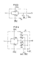
- FIG. 3 shows an exemplary embodiment of the logic circuit 26 which is connected downstream of the carry output 5 of AD n-2 .
- it contains two switching transistors 54 and 55 with their switching paths in parallel, the first of which is designed as a P-channel field-effect transistor and the second as an N-channel field-effect transistor.
- the source connections of these transistors are connected to the input of the logic circuit 26, which is connected to the carry output 5 of FIG. 1, the drain connections of these transistors to an output 56 of 26, which is connected to the input of the buffer 36.
- the output 56 is connected via a further N-channel switching transistor 57 to a switching point 58 which is at reference potential.
- the gates of 54 and 57 are assigned the ORALL signal, the gate of 55 the inverted signal ORALL .
- the other logic circuits, for example 27, which are connected downstream of the carry outputs of the adders AD n - 3 ... AD o are also expediently designed in accordance with FIG. 3.
- FIG. 4 An embodiment of the logic circuit 24 is shown in FIG. 4.
- two switching transistors 58a and 59 are provided with their switching paths in parallel, the source connections of which are connected to a switching point which is connected to the sum output 4 of AD n-2 .
- the drains of 58a and 59 are connected to a node 60, which is the output of 24.
- the circuit point 60 is connected via the series connection of two P-channel switching transistors 61 and 62 to a connection 63, which is connected to the supply voltage.
- 60 is connected to a connection 66 which is at reference potential via the series connection of two N-channel switching transistors 64 and 65.
- the gates of the P-channel transistor 58a and the transistor 64 are controlled via the output 40 with the signal ORALL, the gates of the N-channel transistor 59 and the transistor 62 with the signal which is output via the output 40 'and are inverted for this purpose
- ORALL The gates of 61 and 65 are connected to the output 42 of 28 and are connected with - OVFL acted upon.
- the logic circuit 23 is expediently also constructed in accordance with FIG. 4.
- the logic circuit 25 is advantageously constructed in accordance with FIG. 4, wherein only instead of the signal - OVFL the signal
- + OVFL is used to control the transistors 61 and 65.
- the logic circuits which are connected downstream of the sum outputs of the further adders AD n - 4 ... AD 0 are expediently likewise designed in accordance with the logic circuit 25.
- FIG. 5 shows the development of an arrangement according to FIG. 1, which is used for the bit-parallel addition of four binary numbers in two's complement.
- the group of adders AD i already shown in FIG. 1 is followed by an additional group of adders ZA i , each adder ZA 1 being provided with three inputs.
- the output lines from AD I are omitted Logic circuits 23 to 27 and the latch 33 to 37 connected to the inputs of the adders ZA i .
- the output lines 6 to 8 are each led to the first inputs Z11, Z12 and Z13 of ZA n-1 , ZA n-2 and ZA n - 3 , the output lines 14 and 15 to the second inputs Z21 and Z22 of ZA n -1 and ZA n-2.
- the sum output of an adder AD with the first input of the adder ZA connected downstream; is connected while the carry output from AS; with the second input of the adder ZA i + 1 of the next higher value.
- the additional adders ZA are connected on their lower output sides in the same way and with the same circuit parts as the adders AD i in FIG. 1. These circuit parts are therefore provided with the same reference numerals as in FIG.
- the subtotal word occurring at points 11 ', 12' ..., which is applied to the first inputs of AD i via the intermediate memories 33 ', 34' ..., represents a first binary number, which appears at points 21 ', 22 '... occurring carry word, which is applied to the second inputs of AD i via the intermediate memories 36', 37 '..., a second binary number.
- the number D present at the third inputs of AD i forms a third binary number and a number E applied to the third inputs of the additional adders ZA i forms a fourth binary number.
- the decoder 28 in Depending on the bits at the first two inputs of AD n-1 and AD n-2, it is determined whether there is a positive or negative overflow condition and by means of the logic circuits 23 'to 27' etc., causes the saturation measures already explained with reference to FIG. 1.
- the arrangement according to FIG. 5 can be made in a corresponding manner by adding further adders ZA ; downstream groups of adders can be expanded for an addition of five or more binary numbers in two's complement.
- the circuit parts 23 'to 27' and 33 'to 37' are then provided on the output side by the further adders arranged in the lowest adder group and immediately preceding the adder AS '.
- the recursive circuit branches also run from the outputs of the intermediate memories 33' to 37 '. to the inputs of the adders AD. Circuit arrangements formed from a plurality of adder lines for adding five or more binary numbers are described, for example, in the book "Computer Arithmetic" by K.Hwang, published by John Wiley & Sons, New York, 1979, pp. 100-103, cf. in particular Fig. 4.3, removable.
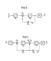
- FIG. 6 shows a first-order recursive filter which contains an accumulator according to FIG. 1.
- a sequence of n-digit binary numbers Di which are respectively applied to the input 67 in successive clock periods and are represented in two's complement and correspond to a sequence of sampled amplitude values of an analog input signal, are initially bit-parallel by one in a delay stage 68, which consists of n buffers Delayed the cycle period and then supplied to the third inputs of the accumulator AD according to FIG. 1.
- the subtotals and carry words derived from this are delayed by a further clock period in a delay stage 69, which consists of the buffers 33 to 37, etc., and are then fed via a recursive loop 70 to the first and second inputs of the accumulator AD i . Both words can be shifted in their assignment to the individual adders AD i to the right or left by m bits, which corresponds to a multiplication by 2 -m or 2 m in an evaluator 70a. The more than 70 words supplied are added to the binary number D present at the third clock of AD i at the next clock cycle.
- the subtotal and carry words occurring at the output of delay stage 69 are fed to adder AS via their inputs 11, 12 ... 21, 22 ... and combined to form the filtered digital output signal Di '.
- FIG. 7 shows a recursive filter of the second order, which differs from FIG. 6 in that. that the subtotals and carry words given by 69 are fed to an accumulator according to FIG. 5, which is labeled AD ;, ZA; is indicated.
- the subtotals and carry words emitted by this are delayed by a clock period in a delay stage 71 (which corresponds to the buffers 33 'to 37') and via a recursive loop 72 both the first two inputs of the accumulator AD i and the first two inputs of the accumulator AD i , ZA i supplied.
- the third input of AD is assigned Di, the third and fourth inputs of AD ; , ZA i with the subtotal and carryover words of 69 of the first accumulator AD;
- the subtotals and carry words occurring at the output of the delay stage 71 are fed to the adder stage AS 'via their input 11', 12 '... 21', 22 'and combined to form the filtered digital output signal Di'.
- An accumulator according to FIG. 2 and n-1 accumulators according to FIG. 5 can be used in an analog manner in a recursive filter of the nth order.
- the buffers 33 to 37 or 33 'to 3T etc. can advantageously be designed as shift register stages, each consisting of master-slave flip-flops. Furthermore, the adding device AS or AS 'can be designed in accordance with the adding device shown in FIG. 9 of patent application P (VPA 85 P 1437 DE) and described in detail there.
- the adder AD n-1 can have a correction element on the output side which carries out an overflow correction which is necessary when relatively large sub-sum and carry words of opposite signs are combined to form a relatively small sum word.
- a correction element replaces the carry word of the adder AD n-2 with the second highest value by the carry bit of the most significant adder AD n-1 and in the event that the carry bits of the two most significant adders AD n-1 and AD n-2 are different the sum bit of AD n-1 is replaced by the carry bit of AD n-1 .
- Such overflow correction measures are described in detail in patent application P (VPA 85 P 1437 DE).
- each group in addition to the two most significant adders, for example AD n-1 and AD n-2, each group can also have other adders of subsequent valencies, for example AD n-3 and AD n-4, can each be assigned one and the same bit of a supplied binary number D or E via their third inputs. This then corresponds to a sign multiplication of the binary numbers represented in two's complement.
Landscapes
- Engineering & Computer Science (AREA)
- Physics & Mathematics (AREA)
- General Physics & Mathematics (AREA)
- Theoretical Computer Science (AREA)
- Pure & Applied Mathematics (AREA)
- Mathematical Analysis (AREA)
- Computational Mathematics (AREA)
- Computing Systems (AREA)
- Mathematical Optimization (AREA)
- General Engineering & Computer Science (AREA)
- Complex Calculations (AREA)
- Compression, Expansion, Code Conversion, And Decoders (AREA)
- Processing Of Color Television Signals (AREA)
Applications Claiming Priority (2)
| Application Number | Priority Date | Filing Date | Title |
|---|---|---|---|
| DE3524981 | 1985-07-12 | ||
| DE19853524981 DE3524981A1 (de) | 1985-07-12 | 1985-07-12 | Anordnung mit einem saettigbaren carry-save-addierer |
Publications (3)
| Publication Number | Publication Date |
|---|---|
| EP0209014A2 true EP0209014A2 (fr) | 1987-01-21 |
| EP0209014A3 EP0209014A3 (en) | 1990-05-09 |
| EP0209014B1 EP0209014B1 (fr) | 1993-05-19 |
Family
ID=6275647
Family Applications (1)
| Application Number | Title | Priority Date | Filing Date |
|---|---|---|---|
| EP86109135A Expired - Lifetime EP0209014B1 (fr) | 1985-07-12 | 1986-07-04 | Dispositif ayant un additionneur à réservation de retenue saturable |
Country Status (5)
| Country | Link |
|---|---|
| US (1) | US4819198A (fr) |
| EP (1) | EP0209014B1 (fr) |
| JP (1) | JPH0814789B2 (fr) |
| AU (1) | AU592099B2 (fr) |
| DE (2) | DE3524981A1 (fr) |
Cited By (1)
| Publication number | Priority date | Publication date | Assignee | Title |
|---|---|---|---|---|
| DE4403917C2 (de) * | 1993-02-19 | 1999-06-02 | Hewlett Packard Co | Vorrichtung zum Berechnen einer Bit-Besetzungszählung |
Families Citing this family (16)
| Publication number | Priority date | Publication date | Assignee | Title |
|---|---|---|---|---|
| ATE93635T1 (de) * | 1986-06-10 | 1993-09-15 | Siemens Ag | Anordnung zur bitparallelen addition von binaerzahlen mit carry-save ueberlaufkorrektur. |
| US5047975A (en) * | 1987-11-16 | 1991-09-10 | Intel Corporation | Dual mode adder circuitry with overflow detection and substitution enabled for a particular mode |
| DE68909618T2 (de) * | 1988-01-09 | 1994-05-05 | Sumitomo Bakelite Co | Verfahren zur Herstellung eines mit einer Dünnschicht aus Metalloxid überzogenen durchsichtigen leitenden Films. |
| JPH0391832A (ja) * | 1989-09-05 | 1991-04-17 | Sony Corp | 加算回路 |
| US5038314A (en) * | 1989-11-17 | 1991-08-06 | Digital Equipment Corporation | Method and apparatus for correction of underflow and overflow |
| US5272659A (en) * | 1990-06-26 | 1993-12-21 | Allied-Signal Inc. | Engine control with fixed point digital overflow prevention |
| US5164914A (en) * | 1991-01-03 | 1992-11-17 | Hewlett-Packard Company | Fast overflow and underflow limiting circuit for signed adder |
| JP2758999B2 (ja) * | 1991-04-10 | 1998-05-28 | 株式会社神戸製鋼所 | 真空アーク蒸着装置 |
| JPH0514510U (ja) * | 1991-08-05 | 1993-02-26 | 内山工業株式会社 | バルブステムの潤滑構造 |
| JPH07168696A (ja) * | 1993-10-19 | 1995-07-04 | Mitsubishi Electric Corp | 2進数加算器のオーバフロー,アンダフロー処理回路 |
| US6219688B1 (en) * | 1993-11-30 | 2001-04-17 | Texas Instruments Incorporated | Method, apparatus and system for sum of plural absolute differences |
| TW421757B (en) * | 1996-06-06 | 2001-02-11 | Matsushita Electric Industrial Co Ltd | Arithmetic processor |
| US5889689A (en) * | 1997-09-08 | 1999-03-30 | Lucent Technologies Inc. | Hierarchical carry-select, three-input saturation |
| US7051062B2 (en) * | 2002-09-10 | 2006-05-23 | Analog Devices, Inc. | Apparatus and method for adding multiple-bit binary-strings |
| GB2396708B (en) | 2002-12-05 | 2006-06-21 | Micron Technology Inc | Hybrid arithmetic logic unit |
| US7962538B2 (en) * | 2005-12-21 | 2011-06-14 | International Business Machines Corporation | Method of operand width reduction to enable usage of narrower saturation adder |
Family Cites Families (12)
| Publication number | Priority date | Publication date | Assignee | Title |
|---|---|---|---|---|
| US3290493A (en) * | 1965-04-01 | 1966-12-06 | North American Aviation Inc | Truncated parallel multiplication |
| US3340388A (en) * | 1965-07-12 | 1967-09-05 | Ibm | Latched carry save adder circuit for multipliers |
| US3515344A (en) * | 1966-08-31 | 1970-06-02 | Ibm | Apparatus for accumulating the sum of a plurality of operands |
| US3609568A (en) * | 1970-06-08 | 1971-09-28 | Bell Telephone Labor Inc | Stable digital filter apparatus |
| US4104729A (en) * | 1975-08-27 | 1978-08-01 | International Standard Electric Corporation | Digital multiplier |
| US4110832A (en) * | 1977-04-28 | 1978-08-29 | International Business Machines Corporation | Carry save adder |
| NL7712367A (nl) * | 1977-11-10 | 1979-05-14 | Philips Nv | Digitaal optelrekenorgaan. |
| US4228520A (en) * | 1979-05-04 | 1980-10-14 | International Business Machines Corporation | High speed multiplier using carry-save/propagate pipeline with sparse carries |
| JPS5674774A (en) * | 1979-11-22 | 1981-06-20 | Nec Corp | Arithmetic circuit with overflow detector |
| JPS56114071A (en) * | 1980-02-13 | 1981-09-08 | Nec Corp | Arithmetic circuit |
| FR2559285B1 (fr) * | 1984-02-03 | 1986-04-25 | Efcis | Unite arithmetique et logique avec indicateur de debordement |
| US4722066A (en) * | 1985-07-30 | 1988-01-26 | Rca Corporation | Digital signal overflow correction apparatus |
-
1985
- 1985-07-12 DE DE19853524981 patent/DE3524981A1/de not_active Withdrawn
-
1986
- 1986-07-04 DE DE8686109135T patent/DE3688445D1/de not_active Expired - Fee Related
- 1986-07-04 EP EP86109135A patent/EP0209014B1/fr not_active Expired - Lifetime
- 1986-07-09 US US06/883,657 patent/US4819198A/en not_active Expired - Fee Related
- 1986-07-09 JP JP61161758A patent/JPH0814789B2/ja not_active Expired - Lifetime
- 1986-07-11 AU AU60073/86A patent/AU592099B2/en not_active Ceased
Cited By (1)
| Publication number | Priority date | Publication date | Assignee | Title |
|---|---|---|---|---|
| DE4403917C2 (de) * | 1993-02-19 | 1999-06-02 | Hewlett Packard Co | Vorrichtung zum Berechnen einer Bit-Besetzungszählung |
Also Published As
| Publication number | Publication date |
|---|---|
| DE3688445D1 (de) | 1993-06-24 |
| EP0209014B1 (fr) | 1993-05-19 |
| AU592099B2 (en) | 1990-01-04 |
| AU6007386A (en) | 1987-01-15 |
| EP0209014A3 (en) | 1990-05-09 |
| US4819198A (en) | 1989-04-04 |
| JPH0814789B2 (ja) | 1996-02-14 |
| JPS6215633A (ja) | 1987-01-24 |
| DE3524981A1 (de) | 1987-01-22 |
Similar Documents
| Publication | Publication Date | Title |
|---|---|---|
| EP0209014B1 (fr) | Dispositif ayant un additionneur à réservation de retenue saturable | |
| DE4302898C2 (de) | Arithmetische Recheneinheit mit Akkumulierfunktion | |
| EP0086904A1 (fr) | Circuit digital de calcul en parallèle pour des nombres binaires positifs et négatifs | |
| EP0453582A1 (fr) | Filtre médian | |
| DE3940897C2 (de) | Schaltungsanordnung und Verfahren zur Berechnung digitaler Summen in einem Halbleiteraddierer mit Parallelübertrag | |
| EP0051079B1 (fr) | Additionneur/soustracteur binaire parallèle en technique MOS à propagation des retenues et étage d'addition/soustraction approprié | |
| EP0383965A1 (fr) | Multiplicateur | |
| EP0208275B1 (fr) | Dispositif d'addition parallèle par bit de nombres binaires | |
| DE1549508B2 (de) | Anordnung zur uebertragsberechnung mit kurzer signallaufzeit | |
| EP0352549B1 (fr) | Additionneur à sélection de retenue | |
| DE2106763A1 (de) | Dekodierschaltung | |
| EP0257362A1 (fr) | Additionneur | |
| DE3035631A1 (de) | Binaerer mos-paralleladdierer | |
| DE69228623T2 (de) | Redundanz-binäre digitale Operationseinheit | |
| EP0130397A1 (fr) | Appareil de calcul numérique | |
| DE2017132A1 (de) | Binarer Parallel Addierer | |
| EP0333884B1 (fr) | Circuit multiplieur parallèle-série ainsi que ses étages de multiplication et d'addition | |
| EP0088135B1 (fr) | Circuit à transistors à effet de champ, à porte isolée, pour un système un parmi n | |
| DE69622486T2 (de) | Übertragvorgriffsgerät mit alternierender polarität | |
| EP0433315A1 (fr) | Circuits d'addition ou de soustraction d'operandes codes selon un code bcd ou dual | |
| EP0249132B1 (fr) | Montage pour l'addition de bits en parallèle de nombre binaires avec correction de débordement par sauvegarde des retenues | |
| DE1086923B (de) | Binaeres Addierwerk fuer elektronische Rechenanlagen und datenverarbeitende Maschinen | |
| EP0106000A1 (fr) | Circuit digital de suppression des changements d'un signal digital | |
| DE3540800A1 (de) | Binaeraddierer-zelle und aus solchen binaeraddierer-zellen zusammengesetztes schnelles addier- und multiplizierwerk | |
| DE2902488C2 (fr) |
Legal Events
| Date | Code | Title | Description |
|---|---|---|---|
| PUAI | Public reference made under article 153(3) epc to a published international application that has entered the european phase |
Free format text: ORIGINAL CODE: 0009012 |
|
| AK | Designated contracting states |
Kind code of ref document: A2 Designated state(s): DE FR GB IT |
|
| PUAL | Search report despatched |
Free format text: ORIGINAL CODE: 0009013 |
|
| AK | Designated contracting states |
Kind code of ref document: A3 Designated state(s): DE FR GB IT |
|
| 17P | Request for examination filed |
Effective date: 19900919 |
|
| 17Q | First examination report despatched |
Effective date: 19920114 |
|
| GRAA | (expected) grant |
Free format text: ORIGINAL CODE: 0009210 |
|
| AK | Designated contracting states |
Kind code of ref document: B1 Designated state(s): DE FR GB IT |
|
| REF | Corresponds to: |
Ref document number: 3688445 Country of ref document: DE Date of ref document: 19930624 |
|
| ITF | It: translation for a ep patent filed | ||
| ET | Fr: translation filed | ||
| GBT | Gb: translation of ep patent filed (gb section 77(6)(a)/1977) |
Effective date: 19930727 |
|
| PLBE | No opposition filed within time limit |
Free format text: ORIGINAL CODE: 0009261 |
|
| STAA | Information on the status of an ep patent application or granted ep patent |
Free format text: STATUS: NO OPPOSITION FILED WITHIN TIME LIMIT |
|
| 26N | No opposition filed | ||
| PGFP | Annual fee paid to national office [announced via postgrant information from national office to epo] |
Ref country code: GB Payment date: 19970620 Year of fee payment: 12 |
|
| PGFP | Annual fee paid to national office [announced via postgrant information from national office to epo] |
Ref country code: FR Payment date: 19971029 Year of fee payment: 12 |
|
| PG25 | Lapsed in a contracting state [announced via postgrant information from national office to epo] |
Ref country code: GB Free format text: LAPSE BECAUSE OF NON-PAYMENT OF DUE FEES Effective date: 19980704 |
|
| PGFP | Annual fee paid to national office [announced via postgrant information from national office to epo] |
Ref country code: DE Payment date: 19980917 Year of fee payment: 13 |
|
| GBPC | Gb: european patent ceased through non-payment of renewal fee |
Effective date: 19980704 |
|
| PG25 | Lapsed in a contracting state [announced via postgrant information from national office to epo] |
Ref country code: FR Free format text: LAPSE BECAUSE OF NON-PAYMENT OF DUE FEES Effective date: 19990331 |
|
| REG | Reference to a national code |
Ref country code: FR Ref legal event code: ST |
|
| PG25 | Lapsed in a contracting state [announced via postgrant information from national office to epo] |
Ref country code: DE Free format text: LAPSE BECAUSE OF NON-PAYMENT OF DUE FEES Effective date: 20000503 |
|
| PG25 | Lapsed in a contracting state [announced via postgrant information from national office to epo] |
Ref country code: IT Free format text: LAPSE BECAUSE OF NON-PAYMENT OF DUE FEES;WARNING: LAPSES OF ITALIAN PATENTS WITH EFFECTIVE DATE BEFORE 2007 MAY HAVE OCCURRED AT ANY TIME BEFORE 2007. THE CORRECT EFFECTIVE DATE MAY BE DIFFERENT FROM THE ONE RECORDED. Effective date: 20050704 |