EP0352730A2 - Dispositif de mémoire semi-conducteur muni d'un système de détection des positions utilisant une structure redondante - Google Patents
Dispositif de mémoire semi-conducteur muni d'un système de détection des positions utilisant une structure redondante Download PDFInfo
- Publication number
- EP0352730A2 EP0352730A2 EP89113687A EP89113687A EP0352730A2 EP 0352730 A2 EP0352730 A2 EP 0352730A2 EP 89113687 A EP89113687 A EP 89113687A EP 89113687 A EP89113687 A EP 89113687A EP 0352730 A2 EP0352730 A2 EP 0352730A2
- Authority
- EP
- European Patent Office
- Prior art keywords
- redundant
- circuit
- memory cell
- normal
- memory cells
- Prior art date
- Legal status (The legal status is an assumption and is not a legal conclusion. Google has not performed a legal analysis and makes no representation as to the accuracy of the status listed.)
- Granted
Links
Images



Classifications
-
- G—PHYSICS
- G11—INFORMATION STORAGE
- G11C—STATIC STORES
- G11C29/00—Checking stores for correct operation ; Subsequent repair; Testing stores during standby or offline operation
- G11C29/70—Masking faults in memories by using spares or by reconfiguring
- G11C29/78—Masking faults in memories by using spares or by reconfiguring using programmable devices
- G11C29/835—Masking faults in memories by using spares or by reconfiguring using programmable devices with roll call arrangements for redundant substitutions
-
- G—PHYSICS
- G11—INFORMATION STORAGE
- G11C—STATIC STORES
- G11C29/00—Checking stores for correct operation ; Subsequent repair; Testing stores during standby or offline operation
- G11C29/04—Detection or location of defective memory elements, e.g. cell constructio details, timing of test signals
- G11C29/08—Functional testing, e.g. testing during refresh, power-on self testing [POST] or distributed testing
- G11C29/12—Built-in arrangements for testing, e.g. built-in self testing [BIST] or interconnection details
- G11C29/44—Indication or identification of errors, e.g. for repair
-
- G—PHYSICS
- G11—INFORMATION STORAGE
- G11C—STATIC STORES
- G11C7/00—Arrangements for writing information into, or reading information out from, a digital store
- G11C7/20—Memory cell initialisation circuits, e.g. when powering up or down, memory clear, latent image memory
Definitions
- the present invention relates to a semiconductor memory device having a redundant structure, and more particularly to a system for detecting the memory cell positions using the redundant structure.
- the redundant circuit has a redundant column or row of memory cells which are added for a normal memory cell array and a redundant decoder for selecting the redundant column or row of memory cells. If the normal memory cell array contains any defective memory cells in a column or a row, the address corresponding to the defective column or row of memory cells is programmed into the redundant decoder in a known manner, thereby replacing the defective column or row of memory cells with the redundant column or row of memory cells, and thus enabling the defective chip to be relieved.
- a memory device having such a redundant circuit involves necessity to know information about relief of the memory cell, that is whether or not the redundant circuit has been actually used, and the address of a defective part in the normal memory cell array which has been replaced with the redundant column or row, when the memory is evaluated or tested.
- Conventional practices therefor include a roll call circuit which is arranged such that a special circuit is provided in a memory chip to obtain relief information.
- the memory circuit consumes an operating current which also flows between the two power voltage terminals.
- the series circuit always consumes some current flowing therethrough at least when the memory circuit is enabled in a case where the redundant circuit is used. This consumes a wasteful power.
- a semiconductor memory device comprises a plurality of normal memory cells arranged in an array, at least one redundant memory cell, means for receiving address information, a selection circuit coupled to the array of the normal memory cells and the redundant memory cell, the selection circuit operatively selecting one memory cell from the array of the normal memory cells in accordance with the address information when the normal memory cell corresponding to the address information is operable and selecting the redundant memory cell when the normal memory cell corresponding to the address information is defective, a read-write circuit coupled to the selection circuit for performing a read operation of the selected memory cell in a read mode and a write operation to the selected memory cell in a write operation, a power voltage terminal for receiving a power voltage, a detection circuit coupled to the power voltage terminal for generating a detection signal when the power voltage is initiated to be applied the power voltage terminal, a first initializing circuit for setting the normal memory cells at a first logic state in response to the detection signal, and a second initializing circuit for setting the redundant memory cell.at a second logic state different from the first logic state in response to
- the normal memory cells and the redundant memory cell are automatically initialized in different logic states, respectively upon the application of the power voltage to the memory circuit. Therefore, the address of the defective memory cell which is replaced by the redundant memory cell can be detected by simply checking read-out data. Any wasteful current does not flow for showing the using state of the redundant memory cell.
- a program circuit 1 includes a series connection of a fuse F and an N-channel MOS field effect transistor Q1 connected between a power voltage terminal Vcc and a reference voltage terminal (GND) and a feed-back inverter IV1 to form a fuse type flip-flop.
- the fuse F is cut when a redundant circuit including a redundant word line WLR, a redundant row decoder 4, a gate 5 and an inverter IV2 is utilized for replacing a defective word of a normal memory cell array (not shown in Fig. 1). Therefore, a signal EN is set at a high level. To the contrary, when the normal memory array is perfectly good and the redundant circuit is not used, the fuse F is not cut to produce a low level of the signal EN.
- the address of a defective part e.g. word line to be replaced with a redundant word line WLR is programmed in the redundant decoder 4 in a known way.
- a first roll-call circuit 2 having a P-channel MOS (PMOS) transistor Q3 and an N-channel MOS (NMOS) transistor Q4 causes a current flowing therethrough between Vcc and GND when the signal EN is at the high level.
- a second roll-call circuit 3 including a PMOS transistor Q5 and an NMOS transistor Q6 connected between Vcc and GND and causes a current flowing between Vcc and GND when the redundant word line is selected.
- the signal EN is at the high level and therefore Q4 is ON, so that the roll call circuit 2 constantly generates a current from the power supply to the ground (GND). For this reason, the current consumption is greater than in a memory in which the redundant circuit is not used by an amount corresponding to the current flowing through the roll call circuit 2.
- the memory device comprises a normal memory array having a plurality of normal memory cells MC, a plurality of word lines WL l - WL m arranged in rows, and a plurality of pairs of bit lines BL, BL (in the drawing, only i-th pair of bit lines BLi, BL i are representatively shown), and a redundant array of redundant memory cells MC′ coupled to the word lines WL l - WL m and a pair of redundant bit lines BL , BL R .
- a redundant column of memory cell MC′ are provided for replacing a defective column of memory cells of the normal memory array.
- Each of the memory cells MC and the redundant memory cells MC′ is constructed as shown in Fig. 4.
- the memory cells MC and MC′ include a flip-flop composed of load resistors R1, R2 and a pair of NMOS transistors Q M1 , Q M1 , and a pair of transfer gate NMOS transistors Q M3 , Q M4 coupled to one word line WL and a pair of bit lines BL, BL .
- a plurality of row decoders 11-l to 11-m are provided for selecting the word lines WL l WL m , respectively.
- the pairs of bit lines BL i , BL i , BL R , BL R are connected to a pair of bus lines DB, DB connected to a read-write circuit 13 connected to an input/output terminal I/O through a plurality of pairs of transfer gate NMOS transistors QY i , QY i ′, QY R . QY R ′.
- Each pair of transfer gate transistors (QY i , QY i ′) are selected by the corresponding column decoder (12-i) and the pair of transistors QY R , QY R ′ for the redundant column are selected by the redundant column decoder 12-R.
- the redundant column decoder 12-R is enabled in response to the high level of the signal EN generated from the program circuit 1 such as shown in Fig. 1 and generates an active (high) level of output Y R when column address information ARY indicates a defective column of the normal array.
- the selective level of Y R inhibits operations of the normal column decoders such as 12-i.
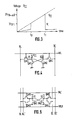
- the memory circuit also includes a power-on detection circuit 10 including PMOS transistor Q11 and NMOS transistors Q12, Q13 connected in series between Vcc and GND and inverters IV3 and IV4.
- the power-on detection 10 a high level pulse signal FC and a low level pulse signal FC when the power voltage Vcc is switched on, as will be explained in detail later.
- Each of the row decoders 11-1 to 11-m includes a NAND gate AGl receiving row address signals ARX, PMOS transistors Q14, Q15, Q16 and NOMS traisnstors Q17 to Q19 and is enabled to select its corresponding word line in accordance with ARX in response to a low level of a control signal XE and selects its corresponding word line irrespective of ARX when the pulse signal FC is at the low level.
- an NMOS transistor Q22 receiving FC at its gate is connected between the true bit line BL i and the ground voltage source and a PMOS transistor Q33 having a gate receiving FC is connected between Vcc and the ground voltage source.
- a PMOS transistor having a gate receiving FC and an NMOS transistor receiving FC at its gate are connected between the true bit line BL R and Vcc and the complementary bit line BL R and the ground voltage source, respectively.
- Load PMOS transistors Q20, Q21, Q24, Q25 for the bit lines BL i , BL i , BL R , BL R are controlled by FC.
- the threshold voltage VTN of the NMOSFET transistors Q12, Q13 is set so as to be greater than the absolute value
- BL i is set at the GND level, while BL i is set at the Vcc level.
- "0" is written into the normal memory cells MC.
- Q24 and Q25 turn OFF, while Q26 and Q27 turn ON, so that BL R is set at the Vcc level, while BL R is set at the GND level.
- "1" is written into the redundant memory cells MC′.
- FC changes from the low level to the high level while FC changes from the high level to the low level
- Q16, Q22, Q23, Q26 and Q27 turn OFF, while Q19 to Q21, Q24 and Q25 turn ON, so that the row decoders and memory cell peripheral circuits become equivalent to those in ordinary memories.
- a redundant row of memory cells MC ⁇ are provided for replacing a defective row of memory cells MC in a normal memory cell array.
- the normal memory cells MC have the same structure as those in Fig. 2, as shown in Fig. 4.
- the redundant row of memory cells MC ⁇ are constructed as shown in Fig. 6. Namely, NMOS transistors Q M5 and Q M6 connected to a control line WL′ and a pair of data set lines BL′ and BL′ of the corresponding column are provided in addition to the memory cells MC shown in Fig. 4.
- the normal row decoders such as 11-j for the normal memory array (MC) have the same structure as those 11-l to 11-m of Fig. 2, while a redundant row decoder 11-R includes PMOS transistors Q31 - Q33 and NMOS transistors Q34 - Q36 and is enabled in response to the low level of XE .
- the output (i.e. WL R ) of the redundant row decoder is forcibly set at the low level in response to the high level of FC.
- the method of obtaining memory relief information in this memory is the same as in the first embodiment, and the memory having a redundant row in this embodiment also exhibits advantageous effects similar to those of the memory having a spare column in the first embodiment.
- the present invention provides a memory circuit having a redundant circuit, comprising a power-on detection circuit which generates a pulse signal when detecting that the power supply has been turned on, and a circuit capable of writing "0" (or “1") into all normal memory cells and "1" (or “0") into all redundant memory cells in synchronism with the pulse signal, whereby it is possible to obtain memory relief information within a short period of time by such an easy method that information stored in the memory cells is read out in the address order after the power supply is switched ON, without any increase in the current consumption which has heretofore been caused by a circuit provided to obtain relief information.
Landscapes
- For Increasing The Reliability Of Semiconductor Memories (AREA)
- Static Random-Access Memory (AREA)
- Techniques For Improving Reliability Of Storages (AREA)
Applications Claiming Priority (2)
| Application Number | Priority Date | Filing Date | Title |
|---|---|---|---|
| JP63186010A JPH0235697A (ja) | 1988-07-26 | 1988-07-26 | メモリ回路 |
| JP186010/88 | 1988-07-26 |
Publications (3)
| Publication Number | Publication Date |
|---|---|
| EP0352730A2 true EP0352730A2 (fr) | 1990-01-31 |
| EP0352730A3 EP0352730A3 (fr) | 1991-03-20 |
| EP0352730B1 EP0352730B1 (fr) | 1994-11-17 |
Family
ID=16180796
Family Applications (1)
| Application Number | Title | Priority Date | Filing Date |
|---|---|---|---|
| EP89113687A Expired - Lifetime EP0352730B1 (fr) | 1988-07-26 | 1989-07-25 | Dispositif de mémoire semi-conducteur muni d'un système de détection des positions utilisant une structure redondante |
Country Status (4)
| Country | Link |
|---|---|
| US (1) | US5008857A (fr) |
| EP (1) | EP0352730B1 (fr) |
| JP (1) | JPH0235697A (fr) |
| DE (1) | DE68919386T2 (fr) |
Cited By (2)
| Publication number | Priority date | Publication date | Assignee | Title |
|---|---|---|---|---|
| EP0405371A3 (en) * | 1989-06-26 | 1991-08-21 | Nec Corporation | Semiconducteur memory device with improved address discriminating circuit for discriminating an address assigned defective memory cell replaced with redundant memory cell |
| US6055647A (en) * | 1997-08-15 | 2000-04-25 | Compaq Computer Corporation | Method and apparatus for determining computer system power supply redundancy level |
Families Citing this family (9)
| Publication number | Priority date | Publication date | Assignee | Title |
|---|---|---|---|---|
| JP2734705B2 (ja) * | 1989-12-25 | 1998-04-02 | 日本電気株式会社 | 半導体記憶装置 |
| JPH04255998A (ja) * | 1991-02-08 | 1992-09-10 | Nec Ic Microcomput Syst Ltd | 半導体記憶装置 |
| JP2816512B2 (ja) * | 1992-07-27 | 1998-10-27 | 三菱電機株式会社 | 半導体記憶装置 |
| EP0665179B1 (fr) * | 1993-12-28 | 2000-05-24 | Sharp Kabushiki Kaisha | Perforateur pour un dispositif de formation d'image |
| JP3530574B2 (ja) * | 1994-05-20 | 2004-05-24 | 株式会社ルネサステクノロジ | 半導体記憶装置 |
| JPH08212797A (ja) * | 1995-01-31 | 1996-08-20 | Nec Corp | 半導体装置 |
| US6262935B1 (en) * | 2000-06-17 | 2001-07-17 | United Memories, Inc. | Shift redundancy scheme for wordlines in memory circuits |
| TW201029012A (en) * | 2009-01-23 | 2010-08-01 | Nanya Technology Corp | Operation method of suppressing current leakage in a memory and access method for the same |
| JP7171286B2 (ja) * | 2018-07-20 | 2022-11-15 | ラピスセミコンダクタ株式会社 | 半導体メモリ装置 |
Family Cites Families (4)
| Publication number | Priority date | Publication date | Assignee | Title |
|---|---|---|---|---|
| US4573146A (en) * | 1982-04-20 | 1986-02-25 | Mostek Corporation | Testing and evaluation of a semiconductor memory containing redundant memory elements |
| JPS61253695A (ja) * | 1985-05-07 | 1986-11-11 | Hitachi Ltd | 半導体記憶装置 |
| JPS63108589A (ja) * | 1986-10-24 | 1988-05-13 | Mitsubishi Electric Corp | 半導体記憶装置 |
| US4885720A (en) * | 1988-04-01 | 1989-12-05 | International Business Machines Corporation | Memory device and method implementing wordline redundancy without an access time penalty |
-
1988
- 1988-07-26 JP JP63186010A patent/JPH0235697A/ja active Pending
-
1989
- 1989-07-25 EP EP89113687A patent/EP0352730B1/fr not_active Expired - Lifetime
- 1989-07-25 DE DE68919386T patent/DE68919386T2/de not_active Expired - Fee Related
-
1990
- 1990-08-08 US US07/563,890 patent/US5008857A/en not_active Expired - Lifetime
Cited By (2)
| Publication number | Priority date | Publication date | Assignee | Title |
|---|---|---|---|---|
| EP0405371A3 (en) * | 1989-06-26 | 1991-08-21 | Nec Corporation | Semiconducteur memory device with improved address discriminating circuit for discriminating an address assigned defective memory cell replaced with redundant memory cell |
| US6055647A (en) * | 1997-08-15 | 2000-04-25 | Compaq Computer Corporation | Method and apparatus for determining computer system power supply redundancy level |
Also Published As
| Publication number | Publication date |
|---|---|
| DE68919386T2 (de) | 1995-06-22 |
| JPH0235697A (ja) | 1990-02-06 |
| EP0352730B1 (fr) | 1994-11-17 |
| EP0352730A3 (fr) | 1991-03-20 |
| DE68919386D1 (de) | 1994-12-22 |
| US5008857A (en) | 1991-04-16 |
Similar Documents
| Publication | Publication Date | Title |
|---|---|---|
| US4612630A (en) | EEPROM margin testing design | |
| US5325325A (en) | Semiconductor memory device capable of initializing storage data | |
| JP4988588B2 (ja) | 静的ランダムアクセスメモリ用のワード線ドライバ回路 | |
| US5384741A (en) | Semiconductor memory device adapted for preventing a test mode operation from undesirably occurring | |
| EP0488612B1 (fr) | Mémoire à semi-conducteur avec capacité pour écriture en retour invertirée et méthode de test se servant d'écriture en retour invertirée | |
| US4744063A (en) | Static memory utilizing transition detectors to reduce power consumption | |
| US5079744A (en) | Test apparatus for static-type semiconductor memory devices | |
| US5463585A (en) | Semiconductor device incorporating voltage reduction circuit therein | |
| KR970006221B1 (ko) | 반도체 기억장치 | |
| US5185722A (en) | Semiconductor memory device having a memory test circuit | |
| US4723227A (en) | Redundant type memory circuit with an improved clock generator | |
| US5343429A (en) | Semiconductor memory device having redundant circuit and method of testing to see whether or not redundant circuit is used therein | |
| US20020060934A1 (en) | Semiconductor memory device and method of identifying programmed defective address thereof | |
| US4984205A (en) | Semiconductor memory device with improved indicator of state of redundant structure | |
| EP0352730B1 (fr) | Dispositif de mémoire semi-conducteur muni d'un système de détection des positions utilisant une structure redondante | |
| US4987560A (en) | Semiconductor memory device | |
| KR0136448B1 (ko) | 에러 자체 정정회로를 갖는 반도체 메모리 소자 | |
| EP0740308B1 (fr) | Dispositif de mémoire dynamique à semi-conducteur | |
| JPH05250896A (ja) | 半導体記憶装置及びそれに用いる検知回路 | |
| US5229966A (en) | Current control circuit for dynamic memory | |
| KR20010086264A (ko) | 반도체 기억 장치 | |
| US6307772B1 (en) | Static type semiconductor memory device for lower current consumption | |
| JPH0793997A (ja) | スタティック型半導体記憶装置 | |
| JPH04276392A (ja) | 半導体記憶装置 | |
| US6535441B2 (en) | Static semiconductor memory device capable of accurately detecting failure in standby mode |
Legal Events
| Date | Code | Title | Description |
|---|---|---|---|
| PUAI | Public reference made under article 153(3) epc to a published international application that has entered the european phase |
Free format text: ORIGINAL CODE: 0009012 |
|
| 17P | Request for examination filed |
Effective date: 19890725 |
|
| AK | Designated contracting states |
Kind code of ref document: A2 Designated state(s): DE FR GB |
|
| PUAL | Search report despatched |
Free format text: ORIGINAL CODE: 0009013 |
|
| AK | Designated contracting states |
Kind code of ref document: A3 Designated state(s): DE FR GB |
|
| 17Q | First examination report despatched |
Effective date: 19931229 |
|
| GRAA | (expected) grant |
Free format text: ORIGINAL CODE: 0009210 |
|
| AK | Designated contracting states |
Kind code of ref document: B1 Designated state(s): DE FR GB |
|
| REF | Corresponds to: |
Ref document number: 68919386 Country of ref document: DE Date of ref document: 19941222 |
|
| ET | Fr: translation filed | ||
| PLBE | No opposition filed within time limit |
Free format text: ORIGINAL CODE: 0009261 |
|
| STAA | Information on the status of an ep patent application or granted ep patent |
Free format text: STATUS: NO OPPOSITION FILED WITHIN TIME LIMIT |
|
| 26N | No opposition filed | ||
| REG | Reference to a national code |
Ref country code: GB Ref legal event code: IF02 |
|
| REG | Reference to a national code |
Ref country code: GB Ref legal event code: 732E |
|
| REG | Reference to a national code |
Ref country code: FR Ref legal event code: TQ |
|
| REG | Reference to a national code |
Ref country code: GB Ref legal event code: 732E |
|
| REG | Reference to a national code |
Ref country code: FR Ref legal event code: TP |
|
| PGFP | Annual fee paid to national office [announced via postgrant information from national office to epo] |
Ref country code: DE Payment date: 20070719 Year of fee payment: 19 |
|
| PGFP | Annual fee paid to national office [announced via postgrant information from national office to epo] |
Ref country code: GB Payment date: 20070725 Year of fee payment: 19 |
|
| PGFP | Annual fee paid to national office [announced via postgrant information from national office to epo] |
Ref country code: FR Payment date: 20070710 Year of fee payment: 19 |
|
| GBPC | Gb: european patent ceased through non-payment of renewal fee |
Effective date: 20080725 |
|
| PG25 | Lapsed in a contracting state [announced via postgrant information from national office to epo] |
Ref country code: DE Free format text: LAPSE BECAUSE OF NON-PAYMENT OF DUE FEES Effective date: 20090203 |
|
| REG | Reference to a national code |
Ref country code: FR Ref legal event code: ST Effective date: 20090331 |
|
| PG25 | Lapsed in a contracting state [announced via postgrant information from national office to epo] |
Ref country code: GB Free format text: LAPSE BECAUSE OF NON-PAYMENT OF DUE FEES Effective date: 20080725 |
|
| PG25 | Lapsed in a contracting state [announced via postgrant information from national office to epo] |
Ref country code: FR Free format text: LAPSE BECAUSE OF NON-PAYMENT OF DUE FEES Effective date: 20080731 |