EP0352801B1 - Production method of a semiconductor-on-insulator structure with gettering sites - Google Patents
Production method of a semiconductor-on-insulator structure with gettering sites Download PDFInfo
- Publication number
- EP0352801B1 EP0352801B1 EP89113909A EP89113909A EP0352801B1 EP 0352801 B1 EP0352801 B1 EP 0352801B1 EP 89113909 A EP89113909 A EP 89113909A EP 89113909 A EP89113909 A EP 89113909A EP 0352801 B1 EP0352801 B1 EP 0352801B1
- Authority
- EP
- European Patent Office
- Prior art keywords
- substrate
- layer
- semiconductor
- insulator
- semiconductor substrate
- Prior art date
- Legal status (The legal status is an assumption and is not a legal conclusion. Google has not performed a legal analysis and makes no representation as to the accuracy of the status listed.)
- Expired - Lifetime
Links
Images




Classifications
-
- H—ELECTRICITY
- H10—SEMICONDUCTOR DEVICES; ELECTRIC SOLID-STATE DEVICES NOT OTHERWISE PROVIDED FOR
- H10D—INORGANIC ELECTRIC SEMICONDUCTOR DEVICES
- H10D62/00—Semiconductor bodies, or regions thereof, of devices having potential barriers
- H10D62/80—Semiconductor bodies, or regions thereof, of devices having potential barriers characterised by the materials
- H10D62/83—Semiconductor bodies, or regions thereof, of devices having potential barriers characterised by the materials being Group IV materials, e.g. B-doped Si or undoped Ge
- H10D62/834—Semiconductor bodies, or regions thereof, of devices having potential barriers characterised by the materials being Group IV materials, e.g. B-doped Si or undoped Ge further characterised by the dopants
-
- H—ELECTRICITY
- H10—SEMICONDUCTOR DEVICES; ELECTRIC SOLID-STATE DEVICES NOT OTHERWISE PROVIDED FOR
- H10D—INORGANIC ELECTRIC SEMICONDUCTOR DEVICES
- H10D62/00—Semiconductor bodies, or regions thereof, of devices having potential barriers
- H10D62/80—Semiconductor bodies, or regions thereof, of devices having potential barriers characterised by the materials
- H10D62/85—Semiconductor bodies, or regions thereof, of devices having potential barriers characterised by the materials being Group III-V materials, e.g. GaAs
- H10D62/854—Semiconductor bodies, or regions thereof, of devices having potential barriers characterised by the materials being Group III-V materials, e.g. GaAs further characterised by the dopants
-
- H—ELECTRICITY
- H10—SEMICONDUCTOR DEVICES; ELECTRIC SOLID-STATE DEVICES NOT OTHERWISE PROVIDED FOR
- H10P—GENERIC PROCESSES OR APPARATUS FOR THE MANUFACTURE OR TREATMENT OF DEVICES COVERED BY CLASS H10
- H10P36/00—Gettering within semiconductor bodies
- H10P36/03—Gettering within semiconductor bodies within silicon bodies
-
- H—ELECTRICITY
- H10—SEMICONDUCTOR DEVICES; ELECTRIC SOLID-STATE DEVICES NOT OTHERWISE PROVIDED FOR
- H10P—GENERIC PROCESSES OR APPARATUS FOR THE MANUFACTURE OR TREATMENT OF DEVICES COVERED BY CLASS H10
- H10P36/00—Gettering within semiconductor bodies
- H10P36/03—Gettering within semiconductor bodies within silicon bodies
- H10P36/07—Gettering within semiconductor bodies within silicon bodies of silicon-on-insulator structures
-
- H—ELECTRICITY
- H10—SEMICONDUCTOR DEVICES; ELECTRIC SOLID-STATE DEVICES NOT OTHERWISE PROVIDED FOR
- H10P—GENERIC PROCESSES OR APPARATUS FOR THE MANUFACTURE OR TREATMENT OF DEVICES COVERED BY CLASS H10
- H10P36/00—Gettering within semiconductor bodies
- H10P36/20—Intrinsic gettering, i.e. thermally inducing defects by using oxygen present in the silicon body
-
- H—ELECTRICITY
- H10—SEMICONDUCTOR DEVICES; ELECTRIC SOLID-STATE DEVICES NOT OTHERWISE PROVIDED FOR
- H10P—GENERIC PROCESSES OR APPARATUS FOR THE MANUFACTURE OR TREATMENT OF DEVICES COVERED BY CLASS H10
- H10P90/00—Preparation of wafers not covered by a single main group of this subclass, e.g. wafer reinforcement
- H10P90/19—Preparing inhomogeneous wafers
- H10P90/1904—Preparing vertically inhomogeneous wafers
- H10P90/1906—Preparing SOI wafers
- H10P90/1914—Preparing SOI wafers using bonding
- H10P90/1918—Preparing SOI wafers using bonding including charge trapping layers, e.g. polycrystalline materials
-
- H—ELECTRICITY
- H10—SEMICONDUCTOR DEVICES; ELECTRIC SOLID-STATE DEVICES NOT OTHERWISE PROVIDED FOR
- H10P—GENERIC PROCESSES OR APPARATUS FOR THE MANUFACTURE OR TREATMENT OF DEVICES COVERED BY CLASS H10
- H10P95/00—Generic processes or apparatus for manufacture or treatments not covered by the other groups of this subclass
- H10P95/40—Treatments of semiconductor bodies to modify their internal properties, e.g. to produce internal imperfections
- H10P95/408—Treatments of semiconductor bodies to modify their internal properties, e.g. to produce internal imperfections of Group III-V semiconductors, e.g. to render them semi-insulating
-
- Y—GENERAL TAGGING OF NEW TECHNOLOGICAL DEVELOPMENTS; GENERAL TAGGING OF CROSS-SECTIONAL TECHNOLOGIES SPANNING OVER SEVERAL SECTIONS OF THE IPC; TECHNICAL SUBJECTS COVERED BY FORMER USPC CROSS-REFERENCE ART COLLECTIONS [XRACs] AND DIGESTS
- Y10—TECHNICAL SUBJECTS COVERED BY FORMER USPC
- Y10S—TECHNICAL SUBJECTS COVERED BY FORMER USPC CROSS-REFERENCE ART COLLECTIONS [XRACs] AND DIGESTS
- Y10S428/00—Stock material or miscellaneous articles
- Y10S428/901—Printed circuit
Definitions
- the present invention generally relates to a method of producing substrates having semiconductor-on-insulator structures and production methods thereof, and more particularly to a substrate having a semiconductor-on-insulator structure with gettering sites.
- EP-A1-0133954 discloses a method for manufacturing a semiconductor device, comprising the steps of: forming a first thin single-crystal semiconductor layer on an oxygen-doped semiconductor substrate of one conductivity type, said first layer having one conductivity type and a higher resistivity than that of said semiconductor substrate; ion-implanting an electrically inactive impurity in said first layer, forming a second thin single-crystal semiconductor layer on said first layer, said second layer having one conductivity type and a higher resistivity than that of said semiconductor substrate; performing annealing at a temperature of 550°C to 900°C for not less than four hours after the electrically inactive impurity is ion-implanted; and forming elements on said second layer.
- a substrate having a silicon-on-insulator (SOI) structure (hereinafter simply referred to as an SOI substrate) is effectively used as a semiconductor crystalline substrate for realizing a high-speed operation of a semiconductor device.
- SOI substrate silicon-on-insulator
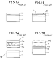
- the SOI substrate As methods of forming the SOI substrate, there basically are two methods. According to a first method, an SOI substrate is first formed, and a gettering site is formed thereafter.
- the SOI substrate comprises a substrate 1, a silicon dioxide (SiO2) layer 2 which is formed on the substrate 1, and a silicon (Si) layer which is formed on the SiO2 layer 2.
- This SOI substrate is subjected to a thermal process so as to form a gettering site 4 in the Si layer 3 as shown in FIG.1B.
- the coefficients of thermal expansion of SiO2 and Si are different, and it is undesirable to subject the SOI substrate to the thermal process which is carried out at a relatively high temperature in the order of 1400 °C for a relatively long time.
- the gettering site 4 is small and unsatisfactory for carrying out the intended elimination of the crystal defects and impurities from a denuded zone 3a of the Si layer 3.
- a second method two stacked structures respectively made up of a single crystal Si substrate and an SiO2 layer are prepared and the SiO2 layers of the two stacked structures are bonded to form a so-called bonded substrate.
- This method is a more promising method than the first method due to recent improvements in bonding techniques. But it is impossible to realize the gettering function in the SOI substrate which is produced by this second method.
- the extrinsic gettering forms the gettering sites by applying an external distortion to a back surface of the Si semiconductor substrate.
- the intrinsic gettering uses the Si semiconductor substrate which is formed by the Czochralski method, for example. Normally, the Si semiconductor substrate formed by the Czochralski method includes oxygen (O i ) in the order of 1x1018 cm ⁇ 3, and thus, the intrinsic gettering forms the gettering sites by subjecting the Si semiconductor substrate to a thermal process to precipitate SiO2.
- the SiO2 layer exists at the central portion and it is impossible to employ the extrinsic gettering to form the gettering sites.
- the thickness of a single crystal semiconductor layer in which semiconductor elements are formed needs to be in the order of 5 microns, and it is virtually impossible to form both an active layer for forming the semiconductor elements and the gettering sites in this extremely thin single crystal semiconductor layer.
- the Si semiconductor substrate is subjected to a thermal process at a temperature of over 1000 °C so as to diffuse the O i in vicinities of the front and back surfaces of the Si semiconductor substrate and form a denuded zone. Then, a thermal process is carried out at a temperature in a range of 400 °C to 600 °C to form gettering sites. Next, a thermal process is carried out at a temperature of over 1000 °C to grow the gettering sites.
- the semiconductor elements are formed in the denuded zone, but the thickness of the denuded zone is in the order of 20 microns.
- the SiO2 layer 17a and the Si substrate 16 must be polished so as to leave an active layer which has a thickness in the order of 5 microns.
- the gettering site will be removed by the polishing as indicated by a phantom line and only the active layer remains according to this method. Therefore, in the case of the SOI substrate formed by the second method, it is also impossible to employ the intrinsic gettering to form the gettering site.
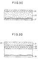
- FIGS.3A through 3E A description will be given of a first embodiment of a production method according to the present invention for producing a first embodiment of a substrate having a semiconductor-on-insulator structure according to the present invention, by referring to FIGS.3A through 3E.
- a Si semiconductor active substrate 21 shown in FIG.3A is prepared by the Czochralski method, for example.
- this active substrate 21 includes O i .
- the active substrate 21 is subjected to a thermal process to form gettering sites 22 which are made of SiO2 as shown in the FIG.3B. No denuded zone is formed by this thermal process.
- the active substrate 21 having the gettering sites 22 is subjected to a thermal process in an oxidizing atmosphere to form a SiO2 layer 23 on a surface of the active substrate 21 as shown in FIG.3C.
- a Si semiconductor base substrate 24 is subjected to a thermal process in an oxidizing atmosphere to form a SiO2 layer 25 on a surface of the base substrate 24, and the SiO2 layer 25 is bonded to the SiO2 layer 23 as shown in FIG.3D.
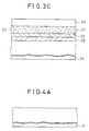
- the active substrate 21 is polished to a predetermined thickness. As a result, a layer of the gettering sites 22 is formed in the active substrate 21 on top of the SiO2 layer 23.
- a Si semiconductor active layer 26 is formed on the active substrate 21 having the layer of the gettering sites 22 as shown in FIG.3E.
- the active layer 26 is formed by an epitaxial growth process.
- this embodiment of the substrate having a semiconductor-on-insulator structure comprises a base stacked structure which is made up of the base substrate 24 and the SiO2 layer 25, and an active stacked structure which is made up of the active substrate 21 and the SiO2 layer 23.
- the base stacked structure and the active stacked structure are bonded by bonding the SiO2 layers 25 and 23, and the active layer 26 is formed on the active substrate 21 which has the layer of the gettering sites 22.
- the layer of the gettering sites 22 is provided under the active layer 26 because the crystal defects and impurities generated within the active layer 26 during the production process of the semiconductor device can be eliminated by the gettering function of the layer of the gettering sites 22. For this reason, it is possible to form semiconductor elements having satisfactory characteristics in the active layer 26.
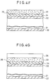
- FIGS.4A through 4G a description will be given of a second embodiment of the production method according to the present invention for producing a second embodiment of the substrate having a semiconductor-on-insulator structure according to the present invention, by referring to FIGS.4A through 4G.
- a base substrate 31 shown in FIG.4A is prepared.
- the substrate 31 is made of a single crystal Si semiconductor.
- the base substrate 31 may be made of other materials such as polysilicon, compound semiconductor, ceramic, refractory metal, and quartz.
- the base substrate 31 is subjected to a thermal process in an oxidizing atmosphere to form a SiO2 layer 32 as shown in FIG.4B.
- the SiO2 layer 32 is formed to a thickness in a range of 0,1 ⁇ m (1000 ⁇ ) to 1 micron.
- a SiO2 layer can be formed directly on the base substrate by an oxidation process carried out after growing a polysilicon layer, a chemical vapor deposition or the like.
- An active substrate 33 shown in FIG.4C is prepared by the Czochralski method.
- the active substrate 33 includes 1x10¹⁷ or more of O i .
- the active substrate 33 is subjected to a thermal process at 450 °C for 5 hours and then to a thermal process at 1100 °C for 1 hour to precipitate and grow gettering sites 35 made of SiO2 as shown in FIG.4D. Then, a thermal process is carried out in an oxidizing atmosphere to form a SiO2 layer 34 on both sides of the substrate 33 to a thickness in the order of 0,2 ⁇ m (2000 ⁇ ).
- the substrates 31 and 33 are bonded by bonding the SiO2 layers 32 and 34 as shown in FIG.4E.
- this bonding is achieved under the following bonding conditions.
- the active stacked structure made up of the SiO2 layer 34 and the active substrate 33 are polished to a thickness of 3 microns, for example. As a result, only the layer of the gettering sites 35 of the active substrate 33 remains on the SiO2 layer 34 which is bonded to the SiO2 layer 32 as shown in FIG.4F.
- a polishing agent comprising Al2O3, a chemical etchant or the like may be used for the polishing process.
- a Si semiconductor active layer 36 is formed on the active substrate 33 which is constituted by the layer of the gettering sites 35 as shown in FIG.4G.
- the active layer 36 is formed by an epitaxial growth process to a thickness of 1 micron. As described before, the crystal defects and impurities generated in the active layer 36 during the production process of the semiconductor device are effectively eliminated by the provision of the layer of the gettering sites 35 under the active layer 36.
- MOS metal oxide semiconductor
- An SOI substrate having a layer of gettering sites with a thickness of 1 micron and an active layer with a thickness of 2 microns was used as the substrate of the present invention, while an SOI substrate having no layer of gettering sites and an active layer with a thickness of 3 microns was used as the conventional SOI substrate.
- Identical MOS diodes were formed in the respective active layers of the two SOI substrates, and life times of minority carriers were measured.
- the life time of minority carriers in the substrate of the present invention was 800 ⁇ 100 microseconds, while the life time of minority carriers in the conventional SOI substrate was 500 ⁇ 200 microseconds. It was thus confirmed that the absolute value of the life time of minority carriers in the present invention is considerably longer compared to that obtained in the conventional SOI substrate, and the deviation in the life time of minority carriers in the present invention is small compared to that of the conventional SOI substrate.
- the substrate has the SOI structure.
- the present invention is of course applicable to any substrate having the semiconductor-on-insulator structure.
- gallium arsenide (GaAs) for the active substrate in place of Si and form a layer of gettering sites in the GaAs active substrate.
- the gettering sites may be formed in the GaAs active substrate by an ion implantation process or the like after the GaAs active substrate is formed on the insulator layer.
- the base substrate may be made of a material other than Si such as polysilicon, silicon carbide, metal, and insulator.
- the insulator layer is also not limited to the SiO2 layer, and the insulator layer may be made of any insulator such as glass and phosphosilicate glass (PSG).
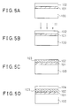
- FIGS.5A through 5C show production steps of a third embodiment of the production method according to the present invention for producing a third embodiment of the substrate having the semiconductor-on-insulator structure according to the present invention.
- a GaAs active substrate (layer) 102 is formed on an insulator layer 101 which is provided on top of a base substrate 100 as shown in FIG.5A.
- the stacked structure shown in FIG.5A is subjected to an ion implantation as shown in FIG.5B to form gettering sites 103 in the GaAs active substrate 102 as shown in FIG.5C.
- a GaAs active layer 104 is formed on the GaAs active substrate 102 which has the gettering sites 103, as shown in FIG.5D.
- CMOS complementary metal oxide semiconductor
- a p-type well 36P and an n-type well 36N are formed in the active layer 36.
- a SiO2 element isolation layer 37 is formed to the SiO2 layer 34 to isolate elements formed in the active layer 36.
- An n-channel transistor formed in the active layer 36 comprises a SiO2 gate insulator layer 38N, a polysilicon gate electrode 39N, an n+-type source region 40N, and an n+-type drain region 41N.
- a p-channel transistor formed in the active layer 36 comprises a SiO2 gate insulator layer 38P, a polysilicon gate electrode 39P, a p+-type source region 40P, and a p+-type drain region 41P.
- this CMOS field effect semiconductor device has the layer of the gettering sites 35 under the p-type well 36P and the n-type well 36N. Hence, it is possible to eliminate the crystal defects and impurities generated during the production process. For example, it is thus possible to prevent a junction leak and a deterioration of the withstand voltage of the gate insulator layers 38N and 38P.
- the n-channel transistor and the p-channel transistor are completely isolated by the SiO2 as in the case of the conventional SOI structure. Therefore, it is possible to easily realize a latch up free device.
- the source regions 40N and 40P and the drain regions 41N and 41P are in contact with the element isolation layer 37 which is made of SiO2, it is possible to suppress the spreading of the depletion layer, make the stray capacitance small and thus realize a high switching speed.
- the bonded substrate is used as the substrate having the semiconductor-on-insulator structure.
- the layer of gettering sites is bonded on the insulator layer of the substrate. It is possible to form the gettering sites in a layer after the layer is formed or bonded on the insulator layer.
Landscapes
- Element Separation (AREA)
- Thin Film Transistor (AREA)
- Recrystallisation Techniques (AREA)
Applications Claiming Priority (2)
| Application Number | Priority Date | Filing Date | Title |
|---|---|---|---|
| JP63186872A JPH0237771A (ja) | 1988-07-28 | 1988-07-28 | Soi基板 |
| JP186872/88 | 1988-07-28 |
Publications (3)
| Publication Number | Publication Date |
|---|---|
| EP0352801A2 EP0352801A2 (en) | 1990-01-31 |
| EP0352801A3 EP0352801A3 (en) | 1990-09-12 |
| EP0352801B1 true EP0352801B1 (en) | 1995-01-18 |
Family
ID=16196151
Family Applications (1)
| Application Number | Title | Priority Date | Filing Date |
|---|---|---|---|
| EP89113909A Expired - Lifetime EP0352801B1 (en) | 1988-07-28 | 1989-07-27 | Production method of a semiconductor-on-insulator structure with gettering sites |
Country Status (5)
| Country | Link |
|---|---|
| US (1) | US5063113A (ja) |
| EP (1) | EP0352801B1 (ja) |
| JP (1) | JPH0237771A (ja) |
| KR (1) | KR930004113B1 (ja) |
| DE (1) | DE68920657T2 (ja) |
Families Citing this family (23)
| Publication number | Priority date | Publication date | Assignee | Title |
|---|---|---|---|---|
| JPH0719839B2 (ja) * | 1989-10-18 | 1995-03-06 | 株式会社東芝 | 半導体基板の製造方法 |
| JP2735407B2 (ja) * | 1990-08-30 | 1998-04-02 | 株式会社東芝 | 半導体装置およびその製造方法 |
| US5366924A (en) * | 1992-03-16 | 1994-11-22 | At&T Bell Laboratories | Method of manufacturing an integrated circuit including planarizing a wafer |
| JP2908150B2 (ja) * | 1992-11-27 | 1999-06-21 | 日本電気株式会社 | Soi基板構造及びその製造方法 |
| US5512375A (en) * | 1993-10-14 | 1996-04-30 | Intevac, Inc. | Pseudomorphic substrates |
| JPH0837286A (ja) * | 1994-07-21 | 1996-02-06 | Toshiba Microelectron Corp | 半導体基板および半導体基板の製造方法 |
| JP2806277B2 (ja) * | 1994-10-13 | 1998-09-30 | 日本電気株式会社 | 半導体装置及びその製造方法 |
| JP2998724B2 (ja) * | 1997-11-10 | 2000-01-11 | 日本電気株式会社 | 張り合わせsoi基板の製造方法 |
| US6255195B1 (en) * | 1999-02-22 | 2001-07-03 | Intersil Corporation | Method for forming a bonded substrate containing a planar intrinsic gettering zone and substrate formed by said method |
| JP4765157B2 (ja) * | 1999-11-17 | 2011-09-07 | 株式会社デンソー | 半導体基板の製造方法 |
| JP5051293B2 (ja) * | 1999-11-17 | 2012-10-17 | 株式会社デンソー | 半導体基板の製造方法 |
| US7273788B2 (en) | 2003-05-21 | 2007-09-25 | Micron Technology, Inc. | Ultra-thin semiconductors bonded on glass substrates |
| US7662701B2 (en) | 2003-05-21 | 2010-02-16 | Micron Technology, Inc. | Gettering of silicon on insulator using relaxed silicon germanium epitaxial proximity layers |
| US7008854B2 (en) * | 2003-05-21 | 2006-03-07 | Micron Technology, Inc. | Silicon oxycarbide substrates for bonded silicon on insulator |
| US7439158B2 (en) * | 2003-07-21 | 2008-10-21 | Micron Technology, Inc. | Strained semiconductor by full wafer bonding |
| JP2006134925A (ja) * | 2004-11-02 | 2006-05-25 | Nec Electronics Corp | Soi基板及びその製造方法 |
| KR100632463B1 (ko) | 2005-02-07 | 2006-10-11 | 삼성전자주식회사 | 에피택셜 반도체 기판의 제조 방법과 이를 이용한 이미지센서의 제조 방법, 에피택셜 반도체 기판 및 이를 이용한이미지 센서 |
| JP2006216934A (ja) * | 2005-02-07 | 2006-08-17 | Samsung Electronics Co Ltd | エピタキシャル半導体基板の製造方法及び半導体装置の製造方法 |
| JP5334354B2 (ja) * | 2005-05-13 | 2013-11-06 | シャープ株式会社 | 半導体装置の製造方法 |
| EP2264753A3 (en) | 2006-06-27 | 2011-04-20 | STMicroelectronics S.r.l. | Integrated device with both SOI insulation and junction insulation and manufacturing method |
| JP2010258083A (ja) | 2009-04-22 | 2010-11-11 | Panasonic Corp | Soiウェーハ、その製造方法および半導体装置の製造方法 |
| JP4685953B2 (ja) * | 2009-07-17 | 2011-05-18 | Dowaエレクトロニクス株式会社 | 横方向を電流導通方向とする電子デバイス用エピタキシャル基板およびその製造方法 |
| JP5882579B2 (ja) * | 2010-12-14 | 2016-03-09 | キヤノン株式会社 | 半導体装置の製造方法 |
Family Cites Families (15)
| Publication number | Priority date | Publication date | Assignee | Title |
|---|---|---|---|---|
| US4288495A (en) * | 1978-05-19 | 1981-09-08 | Ford Motor Company | Article coated with beta silicon carbide and silicon |
| US4226914A (en) * | 1978-05-19 | 1980-10-07 | Ford Motor Company | Novel spraying composition, method of applying the same and article produced thereby |
| JPS5693367A (en) * | 1979-12-20 | 1981-07-28 | Fujitsu Ltd | Manufacture of semiconductor device |
| JPS5717125A (en) * | 1980-07-04 | 1982-01-28 | Oki Electric Ind Co Ltd | Manufacture of semiconductor device |
| US4499147A (en) * | 1981-12-28 | 1985-02-12 | Ibiden Co., Ltd. | Silicon carbide substrates and a method of producing the same |
| US4608095A (en) * | 1983-02-14 | 1986-08-26 | Monsanto Company | Gettering |
| US4608096A (en) * | 1983-04-04 | 1986-08-26 | Monsanto Company | Gettering |
| JPS6031232A (ja) * | 1983-07-29 | 1985-02-18 | Toshiba Corp | 半導体基体の製造方法 |
| US4666532A (en) * | 1984-05-04 | 1987-05-19 | Monsanto Company | Denuding silicon substrates with oxygen and halogen |
| JPS6173345A (ja) * | 1984-09-19 | 1986-04-15 | Toshiba Corp | 半導体装置 |
| JPS6191098A (ja) * | 1984-10-09 | 1986-05-09 | Daido Steel Co Ltd | シリコン基板上における砒素化ガリウム成長結晶体とその結晶成長方法 |
| GB2171555A (en) * | 1985-02-20 | 1986-08-28 | Philips Electronic Associated | Bipolar semiconductor device with implanted recombination region |
| NL8501773A (nl) * | 1985-06-20 | 1987-01-16 | Philips Nv | Werkwijze voor het vervaardigen van halfgeleiderinrichtingen. |
| US4781766A (en) * | 1985-10-30 | 1988-11-01 | Astrosystems, Inc. | Fault tolerant thin-film photovoltaic cell and method |
| JPS6329937A (ja) * | 1986-07-23 | 1988-02-08 | Sony Corp | 半導体基板 |
-
1988
- 1988-07-28 JP JP63186872A patent/JPH0237771A/ja active Granted
-
1989
- 1989-07-21 US US07/382,937 patent/US5063113A/en not_active Expired - Lifetime
- 1989-07-27 DE DE68920657T patent/DE68920657T2/de not_active Expired - Fee Related
- 1989-07-27 KR KR1019890010656A patent/KR930004113B1/ko not_active Expired - Fee Related
- 1989-07-27 EP EP89113909A patent/EP0352801B1/en not_active Expired - Lifetime
Non-Patent Citations (1)
| Title |
|---|
| free devices" * |
Also Published As
| Publication number | Publication date |
|---|---|
| US5063113A (en) | 1991-11-05 |
| KR910003762A (ko) | 1991-02-28 |
| DE68920657T2 (de) | 1995-06-22 |
| KR930004113B1 (ko) | 1993-05-20 |
| DE68920657D1 (de) | 1995-03-02 |
| JPH0237771A (ja) | 1990-02-07 |
| JPH0573349B2 (ja) | 1993-10-14 |
| EP0352801A3 (en) | 1990-09-12 |
| EP0352801A2 (en) | 1990-01-31 |
Similar Documents
| Publication | Publication Date | Title |
|---|---|---|
| US5194395A (en) | Method of producing a substrate having semiconductor-on-insulator structure with gettering sites | |
| EP0352801B1 (en) | Production method of a semiconductor-on-insulator structure with gettering sites | |
| US5663078A (en) | Method for fabricating transistors using crystalline silicon devices on glass | |
| US4500388A (en) | Method for forming monocrystalline semiconductor film on insulating film | |
| JP2894562B2 (ja) | イオン注入による半導体基板に埋込まれた絶縁体の製造方法及び該絶縁体層を含む半導体構造 | |
| US5561303A (en) | Silicon on diamond circuit structure | |
| US4837186A (en) | Silicon semiconductor substrate with an insulating layer embedded therein and method for forming the same | |
| US5218213A (en) | SOI wafer with sige | |
| US4948742A (en) | Method of manufacturing a semiconductor device | |
| JP2560716B2 (ja) | 半導体素子及びその製造方法 | |
| US5760443A (en) | Silicon on insulator with active buried regions | |
| EP0501119B1 (en) | Method of producing semiconductor substrate | |
| US5420458A (en) | Semiconductor device and method of manufacture thereof | |
| DE69225911T2 (de) | Silizium-auf-diamant-schaltungsstruktur und herstellungsverfahren dafür | |
| EP0449589A1 (en) | Method of producing a SOI structure | |
| JPH03129765A (ja) | 半導体装置およびその製造方法 | |
| JPH04355959A (ja) | 半導体装置およびその製造方法 | |
| JP2002359367A (ja) | 半導体基板、その製造方法及び半導体装置 | |
| JP2808701B2 (ja) | 半導体装置の製造方法 | |
| JPH06310427A (ja) | 半導体装置の製造方法 | |
| JPH05166839A (ja) | 半導体装置およびその製造方法 | |
| JP2518378B2 (ja) | 半導体装置の製造方法 | |
| JPH0669430A (ja) | 半導体装置の製造方法 | |
| JPH0587975B2 (ja) | ||
| JPH06188307A (ja) | 半導体装置 |
Legal Events
| Date | Code | Title | Description |
|---|---|---|---|
| PUAI | Public reference made under article 153(3) epc to a published international application that has entered the european phase |
Free format text: ORIGINAL CODE: 0009012 |
|
| AK | Designated contracting states |
Kind code of ref document: A2 Designated state(s): DE FR GB |
|
| PUAL | Search report despatched |
Free format text: ORIGINAL CODE: 0009013 |
|
| AK | Designated contracting states |
Kind code of ref document: A3 Designated state(s): DE FR GB |
|
| 17P | Request for examination filed |
Effective date: 19901115 |
|
| 17Q | First examination report despatched |
Effective date: 19920505 |
|
| GRAA | (expected) grant |
Free format text: ORIGINAL CODE: 0009210 |
|
| AK | Designated contracting states |
Kind code of ref document: B1 Designated state(s): DE FR GB |
|
| REF | Corresponds to: |
Ref document number: 68920657 Country of ref document: DE Date of ref document: 19950302 |
|
| ET | Fr: translation filed | ||
| PLBE | No opposition filed within time limit |
Free format text: ORIGINAL CODE: 0009261 |
|
| STAA | Information on the status of an ep patent application or granted ep patent |
Free format text: STATUS: NO OPPOSITION FILED WITHIN TIME LIMIT |
|
| 26N | No opposition filed | ||
| PGFP | Annual fee paid to national office [announced via postgrant information from national office to epo] |
Ref country code: GB Payment date: 19960718 Year of fee payment: 8 |
|
| PG25 | Lapsed in a contracting state [announced via postgrant information from national office to epo] |
Ref country code: GB Free format text: LAPSE BECAUSE OF NON-PAYMENT OF DUE FEES Effective date: 19970727 |
|
| GBPC | Gb: european patent ceased through non-payment of renewal fee |
Effective date: 19970727 |
|
| PGFP | Annual fee paid to national office [announced via postgrant information from national office to epo] |
Ref country code: FR Payment date: 20040708 Year of fee payment: 16 |
|
| PGFP | Annual fee paid to national office [announced via postgrant information from national office to epo] |
Ref country code: DE Payment date: 20040806 Year of fee payment: 16 |
|
| PG25 | Lapsed in a contracting state [announced via postgrant information from national office to epo] |
Ref country code: DE Free format text: LAPSE BECAUSE OF NON-PAYMENT OF DUE FEES Effective date: 20060201 |
|
| PG25 | Lapsed in a contracting state [announced via postgrant information from national office to epo] |
Ref country code: FR Free format text: LAPSE BECAUSE OF NON-PAYMENT OF DUE FEES Effective date: 20060331 |
|
| REG | Reference to a national code |
Ref country code: FR Ref legal event code: ST Effective date: 20060331 |