EP0353737B1 - Dispositif multiplexeur/démultiplexeur complexe - Google Patents
Dispositif multiplexeur/démultiplexeur complexe Download PDFInfo
- Publication number
- EP0353737B1 EP0353737B1 EP89114274A EP89114274A EP0353737B1 EP 0353737 B1 EP0353737 B1 EP 0353737B1 EP 89114274 A EP89114274 A EP 89114274A EP 89114274 A EP89114274 A EP 89114274A EP 0353737 B1 EP0353737 B1 EP 0353737B1
- Authority
- EP
- European Patent Office
- Prior art keywords
- order group
- clock
- group data
- output
- middle order
- Prior art date
- Legal status (The legal status is an assumption and is not a legal conclusion. Google has not performed a legal analysis and makes no representation as to the accuracy of the status listed.)
- Expired - Lifetime
Links
Images


Classifications
-
- H—ELECTRICITY
- H04—ELECTRIC COMMUNICATION TECHNIQUE
- H04J—MULTIPLEX COMMUNICATION
- H04J3/00—Time-division multiplex systems
- H04J3/02—Details
- H04J3/06—Synchronising arrangements
- H04J3/07—Synchronising arrangements using pulse stuffing for systems with different or fluctuating information rates or bit rates
- H04J3/073—Bit stuffing, e.g. PDH
-
- H—ELECTRICITY
- H04—ELECTRIC COMMUNICATION TECHNIQUE
- H04J—MULTIPLEX COMMUNICATION
- H04J3/00—Time-division multiplex systems
- H04J3/16—Time-division multiplex systems in which the time allocation to individual channels within a transmission cycle is variable, e.g. to accommodate varying complexity of signals, to vary number of channels transmitted
- H04J3/1605—Fixed allocated frame structures
- H04J3/1623—Plesiochronous digital hierarchy [PDH]
- H04J3/1641—Hierarchical systems
-
- H—ELECTRICITY
- H04—ELECTRIC COMMUNICATION TECHNIQUE
- H04J—MULTIPLEX COMMUNICATION
- H04J3/00—Time-division multiplex systems
- H04J3/02—Details
- H04J3/06—Synchronising arrangements
- H04J3/0635—Clock or time synchronisation in a network
- H04J3/0685—Clock or time synchronisation in a node; Intranode synchronisation
Definitions
- the present invention relates to a complex multiplexer/demultiplexer apparatus, more particularly relates to a multiplexer/demultiplexer apparatus which converts low order group data signals to middle order group data signals to multiplex high order group data signals and converts high order group data signals to middle order group data signals to demultiplex low order data signals.
- Telecommunications multiplexer/demultiplexer apparatuses used for exchange systems etc. are able to multiplex a plurality of low order group data signals to obtain a high order group data signal and to demultiplex a high order group data signal to obtain a plurality of low order group data signals.
- low order group data signals mean, for example, first order group data signals
- middle order group data signals and high order group data signals mean, respectively, for example, second order group data signals and third order group data signals.
- the clocks used by the first multiplexer units for performing multiplexing from low order groups to middle order groups for example, seven first multiplexer units corresponding to seven channels
- the timing clocks used by the second demultiplexer units performing multiplexing from middle order groups to low order groups for example, seven second demultiplexer units corresponding to seven channels, were supplied independently from the first demultiplexer units performing demultiplexing from high order groups to middle order groups.
- the present invention has as its object the provision of a complex multiplexer/demultiplexer apparatus which enables a large reduction in the number of timing clock lines connecting the high order group side multiplexer unit and demultiplexer unit to the low order group side multiplexer unit and demultiplexer unit.
- the first aspect of the present invention provides a complex multiplexer/demultiplexer apparatus which comprises: a plurality of first multiplex means which multiplex input low order group data signals to convert them into middle order group data signals, a second multiplex means which multiplexes the middle order group data signals to convert them into high order group data signals, a first demultiplex means which demultiplexes the input high order group data signals to convert them into middle order group data signals, a plurality of second demultiplex means which demultiplex the middle order group data signals to convert them into low order group data signals, and a clock generating means which supplies the timing clocks required by the above means, the multiplexing in the plurality of first multiplexing means being performed based on a comon timing clock synchronized with the timing clock used in the multiplexing in the second multiplexing means, characterised in that a plurality of first speed conversion means are provided corresponding to the first multiplex means and a plurality of second speed conversion means corresponding to the first speed conversion
- a complex multiplexer/demultiplexer apparatus which comprises: a plurality of first multiplexer means (21) which input multiplex low order group data signals to convert them into middle order group data signals, a second multiplex means (22) which multiplexes the middle order group data signals to convert them into high order group data signals, a first demultiplex means (25) which demultiplexes the input high order group data signals, a plurality of second demultiplex means (28) which demultiplex the middle order group data signals to convert them into low order group data signals, and a clock generating means (29) which supplies the timing clocks required by the above means, the demultiplexing in the plurality of second demultiplexing means being performed based on a common timing clock synchronised with the timing clock used in the multiplexing in the second multiplexing means, characterised in that a plurality of first speed conversion means (22) are provided corresponding to the first multiplex means and a plurality of second speed conversion means corresponding to the first speed conversion means are
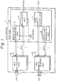
- FIG. 1 is a block diagram of an example of the constitution of a conventional complex multiplexer/demultiplexer apparatus.
- the figure shows the constitution of the telecommunications multiplexer/demultiplexer apparatus (M13 system) which performs multiplexing and demultiplexing between first order group data signals DS1 and third order group data signals DS3.
- M13 system telecommunications multiplexer/demultiplexer apparatus
- the M13 system 11 is provided with seven M12 multiplexer units 12 which multiplex 28 supplied first order group data signals DS1 into seven second order group data signals DS2, seven M12 demultiplexer units 19 which demultiplex the seven second order group data signals DS2 into 28 first order group data signals DS1, and an M23 unit 13 which multiplexes seven second order group data signals DS2 into one third order group data signal DS3 and demultiplexes one third order group data signal DS3 into seven second order group data signals DS2.
- the M23 unit 13 is provided with a clock source 16 which generates basic clock signals of 44.736 MHz, a read clock generating unit 15 which prepares shift clock signals for obtaining synchronization with the output (second order group data signals) of the M12 multiplexer units 12, an M23 multiplexer unit 14 which performs multiplexing of signals, an M23 demultiplexer 17 which performs demultiplexing of signals, and a write clock generating unit 18 which prepares shift clock signals for obtaining synchronization of the signals supplied to the M12 demultiplexer units 19.
- a clock source 16 which generates basic clock signals of 44.736 MHz
- a read clock generating unit 15 which prepares shift clock signals for obtaining synchronization with the output (second order group data signals) of the M12 multiplexer units 12
- an M23 multiplexer unit 14 which performs multiplexing of signals
- an M23 demultiplexer 17 which performs demultiplexing of signals
- a write clock generating unit 18 which prepares shift clock signals for obtaining synchronization
- the read.clock generating unit 15 prepares shift clock signals (Fig. 2) which are supplied respectively to the M12 multiplexer units 12 based on the basic clock signals of 44.736 MHz generated by the clock source 16.
- the respective M12 multiplexer units M12 supply second order group data signals DS2 comprised of four first order group data signals DS1 multiplexed synchronized with the seven shift clock signals prepared by the read clock generating unit 15.
- the M23 multiplexer unit 14 multiplexes the total of seven second order group data signals DS2 supplied from the M12 multiplexer units 12 and outputs a single third order group data signal DS3.
- the M23 demultiplexer unit 17 demultiplexes the supplied third order group data signal DS3 into seven second order group data signals DS2 and supplies the same to the M12 demultiplexer units 19.
- the write clock generating unit 18 prepares shift clock signals supplied to the M12 demultiplexer units 19 based on the reproduction clock signals extracted from the third order group data signals DS3.
- the second order group data signals DS2 output from the M23 demultiplexer unit 17 synchronized with the seven shift clock signals supplied from the write clock generating unit 18 are fetched and demultiplexed into four first order group data signals DS1.
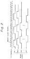
- Figure 2 is a timing chart of portions in the conventional apparatus shown in Fig. 1. That is, it shows the timing of the output of the shift clock signals output from the read clock generating unit 15 of the M23 unit 13. #1 to #7 are a first channel to seventh channel.
- 44.736 MCLK means the basic clock signal of 44.736 MHz which is output from the clock source 16
- read clocks #1 to #7 mean the shift clock signals which are supplied from the read clock generating unit 15 to the M12 multiplexer units 12.
- the signals (first order group data signals and third order group data signals) input to and output from the M13 system 11 are freed of effects of jitter etc. and adjusted in signal speed by stuffing control and destuffing control. Therefore, the second read clock signals shown in Fig. 2 (same for write clock signals from unit 18) have to be prepared separately and supplied to the M12 multiplexer units 12.
- the block shown by the broken line shows the block removed by stuffing control.
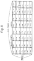
- Figure 3 is a view of the data format of third order group data signals.
- the third order group data signal DS3 of Fig. 1 is, for example, constituted by the data format shown in Fig. 3.
- This data format shows the data signal of one multiframe. The same multiframe is repeated consecutively to form a series of data signals DS3.
- One multiframe consists of seven consecutive subframes. In this case, the end of the front subframe and the head of the following subframe are connected to form the multiframe.
- Each subframe is constituted of eight blocks, each block including 85 bits.
- At the head of each block is inserted a so-called "G" bit.
- G bit
- X1, X2 is an office alarm bit
- F1F0 are subframe frame synchronization bits
- M0, M1 are multiframe frame synchronization bits
- P1, P2 are parity bits
- Cmn is a stuffing indication bit. The m of Cmn shows the channel and the n shows the number of repetitions for the majority decision.
- FIG. 4 is a timing chart showing in further detail the timing chart of Fig. 2. This shows the "G" bits explained in Fig. 3, the master clock of the signal DS3 (same as basic clock signal), and the third order group data signal DS3.
- the point which should be noted in Fig. 4 is that the shift clock signals (#1 to #7) from the read clock generating unit 15 are not completely consecutively shifted (same for write clock generating unit 18). This is because a "G" bit pulse is inserted between the shifts.
- timing clocks are generated corresponding to the channels and have to be supplied for each channel. That is, seven read clock signals are required for readout the second order group data signals from the M12 multiplexer units 12 corresponding to the channels. Further, seven write clock signals are required for supplying second order group data signals to the M12 demultiplexer unit 19. There is consequently much, complicated wiring. This is the problem mentioned earlier.
- the present invention proposes a system for performing the input and output of signals in synchronization with a common clock signal.
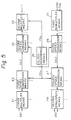
- Figure 5 is a block diagram of the principle of the complex multiplexer/demultiplexer apparatus relating to the present invention.
- the present invention provides complex multiplexer/demultiplexer apparatus which includes: a plurality of first multiplex means 21 which multiplex input first order group data signals DS1 to convert them into middle order group (second order group) data signals DS2, a second multiplex means 24 which multiplexes the middle order group (second order group) data signals DS2 to convert them into high order group (third order group) data signals DS3, a first demultiplex means 25 which demultiplexes the input high order group (third order group) data signals DS3 to convert them into middle order group (second order group) data signals DS2, a plurality of second demultiplex means 28 which demultiplex the middle order group (second order group) data signals DS2 to convert them into low order group (first order group) data signals DS1, and a clock generating means 29 which supplies the timing clocks required by the above means, wherein the second multiplex means 24 operates in synchronization with the basic clock signal CK B prepared by the clock generating means 29, the first multiplex means 21 operates in synchronization with a
- additional information bits are inserted in each empty bit, the additional information bits being at least stuffing indication bits.
- the signals are multiplexed and the plurality of multiplexed signals output from there are further multiplexed by the second multiplex means 24.
- the signals are demultiplexed.
- Each of the demultiplexed signals which are equal in number to the number of channels, are then further demultiplexed at the plurality of second demultiplex means 28.
- the signal speed is converted by insertion of the additional information bits at the signal supply side and the signal speed is converted by deletion of the additional information bits by the signal receiving side.
- FIG. 6A is a view showing illustratively the basic concept of the present invention.
- Figure 6B is a view showing illustratively the basic concept of the prior art.
- reference numerals 12 and 13 correspond to the afore-mentioned M12 multiplexer unit and M23 unit (same in Fig. 6B).
- the M12 multiplexer units 12 of the seven channels receive in common the second order group common clock CK C (6.391 MHz) from the M23 unit. This is converted once to a second order group data clock (6.312 MHz) by the speed conversion means 22, then raised to 6.391 MHz by the insertion of the above-mentioned empty bits and sent to the unit 13.
- the figure of 6.312 MHz is 1.544 MHz x 4, as shown in Fig. 6B.
- the channels send data to the unit 13 at a 6.312 MHz clock.
- the unit 13 periodically generates a sampling S2 in which stuffing bits are inserted. Therefore, in Fig. 6B, a clock transfer line L is required for each channel.
- the clocks of the channels are standardized to 6.391 MHz and it is made possible to receive a single clock CK C (6.391 MHz) from the unit 13.
- the speed conversion means 22 it is necessary to match the second order group data clock (6.312 MHz) and the second order group common clock (6.391 MHz). That is, the speed 6.312 MHz of the second order group data clock is the apparent average speed.
- FIG. 7 is a view showing illustratively the speed conversion based on the present invention.
- the second order group data clock CK D is bit synchronized with the second order group common clock CK C , but due to the empty bit E inserted periodically into the CK D , the apparent speed falls to 6.312 MHz.
- the additional information bit AI is inserted into the empty bit E.
- This additional information bit includes, when necessary, a variable slot bit (V bit) for elimination of jitter.
- the A1 bit is extracted and the additional information (for example, the stuffing control information) is obtained.
- the CK D ′ in the lower section of Fig. 7 shows the bit train in the case of absorption of jitter, while the CK D under that shows the bit train in the case of the jitter not being absorbed.
- Figure 8 is a block diagram showing an embodiment of the present invention.
- the first multiplex means 21 corresponds to the M12 multiplexer unit 31.
- the first speed conversion means 22 corresponds to the speed converter 32.
- the second speed conversion means 23 corresponds to the speed converter 41.
- the second multiplex means 24 corresponds to the M23 multiplexer unit 42.
- the first demultiplex means 25 corresponds to the M23 demultiplexer unit 43.
- the third speed conversion means 26 corresponds to the speed converter 44.
- the fourth speed conversion means 27 corresponds to the speed converter 33.
- the second demultiplex means 28 corresponds to the M12 demultiplexer unit 34.
- the clock generating means 29 corresponds to the clock source 45, the frame timing pulse generating unit 46, and the frequency divider 47.
- the basic clock signal CK B corresponds to the clock signal of 44.736 MHz output from the clock source 45.
- the second order group common clock CK C corresponds to the 6.391 MHz clock signal output from the frequency divider 47.
- the M13 system is provided with seven M12 units 31 which multiplex four first order group data signals DS1 to output second order group data signals DS2 and demultiplex second order group data signals DS2 to give four first order group data signals DS1 and an M23 unit 40 which multiplexes a total of seven second order group data signals DS2 supplied from the M12 units 30 to give third order group data signals DS3 and demultiplexes third order group data signals DS3 to obtain seven second order group data signals DS2 and supply the second order group data signals DS2 to the M12 units 30.
- the M12 units 30 are each provided with an M12 multiplexer unit 31 which multiplexes four first order group data signals DS1, an M12 demultiplexer unit 34 which demultiplexes signals to obtain four first order group data signals DS1, a speed converter 32 which performs speed conversion on signals by insertion of additional information bits (AI), and a speed converter 33 which performs speed conversion on signals by separation (deletion) of the additional information bits.
- an M12 multiplexer unit 31 which multiplexes four first order group data signals DS1
- an M12 demultiplexer unit 34 which demultiplexes signals to obtain four first order group data signals DS1
- a speed converter 32 which performs speed conversion on signals by insertion of additional information bits (AI)
- a speed converter 33 which performs speed conversion on signals by separation (deletion) of the additional information bits.
- the speed converter 32 is supplied with a 6.391 MHz second order group common clock CK C and frame timing pulse FTP (Fig. 11) supplied from the M23 unit 40.
- the speed converter 32 outputs a signal DS2 converted in speed to 6.391 Mbps by insertion of additional information bits into the second order group signals DS2 output from the M12 multiplexer unit 31 based on the clock signals and frame timing pulses.
- a stuffing controlled signal is output from the M12 multiplexer unit 31.
- Speed conversion is performed by addition of specific bit information (stuffing indicator bit variable slot) at a predetermined bit position of this signal. The detailed operation will be explained later.
- the speed converter 33 is supplied with the above-mentioned 6.391 MHz common clock CK C .
- the speed converter 33 separates the additional information bits from the signal supplied from the M23 unit 40 in synchronization with the clock CK C and further performs destuffing control to obtain a second order group data signal and supplies the same to the M12 demultiplexer unit 34.
- the M23 unit 40 is provided with an M23 multiplexer unit 42 which multiplexes seven second order group data signals DS2, an M23 demultiplexer unit 43 which demultiplexes signals to obtain seven second order group data signals DS2, seven speed converters 41 which perform speed conversion on signals by separation of the additional information bits (AI), seven speed converters 44 which perform speed conversion on signals by insertion of additional information bits, a clock source 45 which generates a 44.736 MHz basic clock signal CK B , a frequency divider 47 which divides the basic clock signal output from the clock source 45 to generate a 6.391 MHz second order group common clock CK C , and an FTP generating unit 46 which generates a frame timing pulse (FTP) for obtaining frame synchronization.
- FTP frame timing pulse
- the speed converters 41 correspond to the seven M12 units 30.
- the 6.391 Mbps signals DS2 output from the speed converters 32 are input.
- the speed converters 41 delete the additional information bits from the 6.391 Mbps signals DS2 and supply the 6.312 MHz second order group data signals DS2 obtained by destuffing control to the M23 multiplexer unit 42.
- the speed converters 44 correspond to the seven second order group data signals DS2 separated by the M23 demultiplexer unit 43 and output the signals DS2 converted in speed to 6.391 Mbps by insertion of additional information bits to the 6.312 Mbps second order group data signals input from the M23 demultiplexer unit 43.
- the signals DS2 output from the speed converters 44 are supplied to the speed converters 33 of the M12 units 30.
- the clock source 45 generates a 44.736 MHz clock signal to serve as the basic clock signal CK B and supplies the same to the M23 multiplexer unit 42, the FTP generating unit 46, and the frequency divider 47.
- the M23 multiplexer unit 42 operates in synchronization with the clock signal CK B .
- the FTP generating unit prepares FTP's synchronized with the clock signal in accordance with the multiplexing operation (line L′) in the M23 multiplexer unit 42 and supplies the same to the speed converters 32 of the M12 units 30.
- the frequency divider 47 divides the supplied 44.736 MHz basic clock signal CK B to generate 6.391 MHz second order group common clocks CK C and supplies the same to the speed converters 32 and speed converters 33 of the M12 units 30.
- FIG. 9A and Fig. 9B are views of the specific circuit construction of speed converters. Note that these show the pair of M12 units 30, speed converter 32, and speed converter 33.
- the speed converter 32 is comprised of a clock generating unit 51 which generates a clock signal including empty bits, that is, the second order group data clock CK D , in accordance with a stuffing request supplied from the M12 multiplexer unit 31 and an AI bit insertion unit 52 which inserts the additional information bits AI.
- the clock generating unit 51 receives as input the stuffing request and the 6.391 MHz clock signal, that is, the second order group common clock CK C , and supplies a 6.312 MHz clock signal CK D with empty bits to the M12 multiplexer unit 31.
- the AI bit insertion unit 52 receives as input the 6.312 Mbps (CK D ) second order group data signal output from the M12 multiplexer unit 31 and inserts additional information bits AI to prepare a 6.391 Mbps (CK C ) signal.
- FIG 10 is a view of an example of the data format of a frame including additional information bits.
- the bit trains (AI1..., AI2...) are shown stacked vertically.
- "AI1" to “AI8” show stuffing indicator bits
- "V” shows variable slot bits.
- Stuffing indicator bits (hereinafter referred to as AI bits) are inserted at a rate of one bit per 85 bits (see 85 bits of Fig. 3).
- AI bits are inserted at the 42nd bit. Note that 42 bits are shown as an example. The example shows insertion at about the middle (85/2) of 85 bits.
- the insertion of the AI bits enables common use of the data format of the signal output from the speed converters 32 and the signal speeds.
- variable slot bits V are used for eliminating the effects of jitter, etc. When the data becomes long, these bits are omitted.
- the information on the variable slot bits is included in the AI bits. For example, when the AI bits are all "1", this indicates that valid data is included in the variable slot bit V. When they are all "0", it indicates that the variable slot bits V are omitted.
- the speed converters 41 are comprised of AI bit extraction units 55 which extract additional information bits AI in the input signals, an AI bit deletion unit 53 which deletes the additional information bits, a stuffing detection unit 56 which detects stuffing, and a destuffing control unit 54 which performs destuffing control in accordance with the detected stuffing.
- a 6.391 Mbps (CK C ) signal DS2 is input into the AI bit extraction unit 55, whereupon AI bits (AI1 , AI2 , ...) inserted at a rate of one bit per 85 bits are extracted.
- the AI bit deletion unit 53 sends the signals with the AI bits deleted to the destuffing control unit 54.
- the stuffing detection unit 56 detects stuffing in accordance with the extraction operation of the additional information bits AI in the AI bit extraction unit 55, while the destuffing control unit 54 performs the destuffing control in accordance with stuffing detection.
- the 6.312 Mbps (second order group data clock CKD) second order group data signal DS2 prepared by the destuffing control is supplied to the multiplexer unit 42 where further multiplexing is performed.
- the speed converter 44 includes a first-in first-out unit (FIFO) 61 which temporarily stores the second order group data signals and an AI bit insertion unit 63 which inserts additional information bits AI.
- FIFO first-in first-out unit
- the FIFO unit 61 temporarily stores the 6.312 Mbps (second order group data block CKD) second order group data signals output from the M23 demultiplexer unit 43, then supplies the same to the stuffing control unit 62.
- the stuffing control unit 62 and the AI bit insertion unit 63 are supplied from the M23 demultiplexer unit 43 with information regarding the stuffing bit position. Based on this information, stuffing control is performed at the stuffing control unit 62, then the AI bits and variable slot bits V are inserted by the AI bit insertion unit 63.
- the 6.391 Mbps (second order group common clock CK C ) signal DS2 output from the AI bit insertion unit 63 is supplied to the speed converter 33.
- the speed converter 33 includes an AI bit extraction unit 65 which extracts the additional information bits AI in the input signals DS2, an AI bit deletion unit 67 which deletes the additional information bits, a stuffing detection unit 66 which detects the stuffing, and a destuffing control unit 68 which performs destuffing control in accordance with the detected stuffing, a clock generating unit 64 which generates a clock signal (CK D ) including empty bits in accordance with the detected stuffing.
- an AI bit extraction unit 65 which extracts the additional information bits AI in the input signals DS2
- an AI bit deletion unit 67 which deletes the additional information bits
- a stuffing detection unit 66 which detects the stuffing
- a destuffing control unit 68 which performs destuffing control in accordance with the detected stuffing
- CK D clock signal
- the clock generating unit 64 is supplied with the results of the stuffing detection of the stuffing detection unit 66 and the 6.391 MHz second order group common clock CK C output from the frequency divider 47 and supplies a 6.312 MHz clock signal including empty bits to the M12 demultiplexer unit 34.
- the AI bit extraction unit 65, the stuffing detection unit 66, the AI bit deletion unit 67, and the destuffing control unit 68 act on the 6.391 Mbps (CK C ) signal DS2 output from the speed converter 44 to perform deletion of the additional information bits AI, detection of stuffing, and processing of destuffing, whereby the 6.312 Mbps (CK D ) second order group data signal DS2 is supplied to the M12 demultiplexer unit 34.
- Figure 11 is a timing chart of signals of key portions in Fig. 9A and Fig. 9B.
- “44.736 MCLK” means a 44.736 MHz basic clock signal CK B generated by the clock source 45
- FTP means a frame timing pulse generated by the FTP generating unit 46
- "6.391 MCLK” means a 6.391 MHz frequency divided clock signal (second order group common clock CK C ) generated by the frequency divider 47
- "MUX” means a 6.391 Mbps signal DS2 supplied from the speed converters 32 of the M12 units 30 to the speed converters 41 of the M23 unit 40
- “DEMUX” means the 6.391 Mbps signal DS2 supplied from the speed converters 44 of the M23 unit 40 to the speed converters 33 of the M12 units 30.
- the first AI bit (AI1) is inserted in synchronization with the FTP output from the FTP generating unit 46, then the input and output of the 6.391 Mbps (CK C ) signal DS2 are performed in synchronization with the 6.391 MHz clock signal (CK C ) output from the frequency divider 47.
- this streamlining of the clock supply lines can reduce the number of input and output pins at the time of conversion to an LSI and is effective in increasing the degree of freedom in LSI design.
- the drop/insert function is a function for pulling in and inserting data at the time of relay of signals and is required in apparatuses having signal relay and termination functions.
- Figure 12 is a view for explaining an example of the advantages given by the present invention and shows specifically the drop/insert function.
- data is transferred between a central office and remote offices.
- This repeater office is also called a "HUB" office.
- This "HUB" office has the functions of taking out (drops) data from data lines between the central office and remote offices, inserting data in these data lines, and returning data.
- the data format of the second order group signals is standardized and the same clock signal (6.391) is synchronized with, so it is possible to return the second order group data signal output from the M23 unit 40 and a drop/insert function can be easily realized.
- the return of the second order group data signal is shown by the symbol R.
- Figure 13 is a circuit diagram of a detailed example of the speed converter 32
- Fig. 14 is a circuit diagram showing a detailed example of the speed converter 41
- Fig. 15 is a circuit diagram showing a detailed example of the speed converter 44
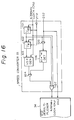
- Fig. 16 is a circuit diagram showing a detailed example of the speed converter 33.
- the speed converter 32 includes a first frequency divider 71 and a second frequency divider 72 which respectively receive the second order group common clock CK C and frame timing pulse FTP and are connected in cascade, a flip flop 74 which receives the output of the second frequency divider 72 as a clock input and is set by the stuffing request pulse, a first variable slot pulse generator 73 which receives as input the output of the second frequency divider 72, the second order group common clock CK C , and the output of the flip flop 74, and a first OR gate 75 which receives as input the output of the first variable slot pulse generator 73, the second order group common clock CK C , and the frame timing pulse FTP, the second order data clock CK D being output from the first OR gate 75.
- the above construction forms the clock generating unit.
- first AND gate 76 which receives as input the output of the first frequency divider 71 and the output of the flip flop 74 and a multiplexer unit 77 which multiplexes the output of the first AND gate 76, the output of the variable slot pulse generator 73, and the second order group data signal DS2 from the corresponding multiplexer unit 31, the output of the multiplexer unit 77 being supplied to the corresponding speed converter 44.
- the speed converter 41 includes a third frequency divider 81 and a fourth frequency divider 82 which respectively receive the second order group common clock CK C and frame timing pulse FTP and are connected in cascade, a second variable slot pulse generator 83 which receives as input the output of the fourth frequency divider 82 and the second order group common clock CK C , a second AND gate 85 which receives as input the output of the third frequency divider 81 and the second order group data signal DS2 from the speed converter 32, an additional information bit detector 86 which receives the output of the second AND gate 85 and detects the additional information bits AI, a third AND gate 84 which receives as input the detection output from the additional information bit detector 86 and the output of the second variable slot pulse generator 83, a second OR gate 88 which receives as input the output of the third AND gate 84, the output of the third frequency divider 81, and the second order group common clock CK C , and an elastic memory (ES) 87 which is subjected to read control by the output of the
- the speed converter 44 includes a first frequency divider 91 and a second frequency divider 92 which respectively receive the second order group common clock CK C and frame timing pulse FTP and are connected in cascade, a flip flop 94 which receives the output of the second frequency divider 92 as a clock input and is set by the generation of the stuffing request, a first variable slot pulse generator 93 which receives as input the output of the second frequency divider 92, the second order group common clock CK C , and the output of the flip flop 94, and a first OR gate 95 which receives as input the output of the first variable slot pulse generator 93, the second order group common clock CK C , and the output of the first frequency divider 91, a phase comparator 96 which receives the output of the first OR gate 95 and the write clock synchronized with the second order group data clock CK D supplied from the demultiplexer unit 43, compares the phase of the two, based on the results of the comparison generates the stuffing request when the phase deviation is
- the speed converter 33 includes a third frequency divider 101 and a fourth frequency divider 102 which respectively receive the second order group common clock CK C and frame timing pulse FTP and are connected in cascade, a second variable slot pulse generator 103 which receives as input the output of the fourth frequency divider 102 and the second order group common clock CK C , a second AND gate 105 which receives as input the output of the third frequency divider 101 and the second order group data signal DS2 from the speed converter 44, an additional information bit detector 106 which receives the output of the second AND gate 105 and detects the additional information bits AI, a third AND gate 104 which receives as input the detection output from the additional information bit detector 106 and the output of the second variable slot pulse generator 103, and a second OR gate 107 which receives as input the output of the third AND gate 104, the output of the third frequency divider 101, the output from the second OR gate 107 being used as the second order group data clock CK D and supplied together with the second order group data signal DS2
Landscapes
- Engineering & Computer Science (AREA)
- Computer Networks & Wireless Communication (AREA)
- Signal Processing (AREA)
- Time-Division Multiplex Systems (AREA)
Claims (22)
- Dispositif multiplexeur/démultiplexeur complexe, comportant:
plusieurs premiers moyens de multiplexage (21) qui multiplexent des signaux d'entrée de données de groupe d'ordre inférieur pour les convertir en signaux de données de groupe d'ordre moyen,
un deuxième moyen de multiplexage (24) qui multiplexe les signaux de données de groupe d'ordre moyen pour les convertir en signaux de données de groupe d'ordre supérieur,
un premier moyen de demultiplexage (25) qui démultiplexe les signaux d'entrée de données de groupe d'ordre supérieur pour les convertir en signaux de données de groupe d'ordre moyen,
plusieurs deuxièmes moyens de démultiplexage (28) qui démultiplexent les signaux de données de groupe d'ordre moyen pour les convertir en signaux de données de groupe d'ordre inférieur, et
un moyen générateur de signaux d'horloge (29) qui fournit l'horloge de synchronisation requise par les moyens ci-dessus,
le multiplexage dans les plusieurs premiers moyens de multiplexage étant effectué sur base d'une horloge de synchronisation commune synchronisée avec l'horloge de synchronisation utilisée dans le multiplexage dans le deuxième moyen de multiplexage, caractérisé en ce que plusieurs premiers moyens de conversion de vitesse (22) sont prévus en correspondance avec les premiers moyens de multiplexage, et en ce que plusieurs deuxièmes moyens de conversion de vitesse (23), correspondant aux premiers moyens de conversion de vitesse, sont prévus du côté du deuxième moyen de multiplexage,
le premier moyen de conversion de vitesse est adapté pour produire les bits vides et le deuxième moyen de conversion de vitesse est adapté pour supprimer les bits vides, les signaux de données de groupe d'ordre moyen étant transférés entre le premier et le deuxième moyens de conversion de vitesse correspondants, synchronisés avec l'horloge commune de groupe d'ordre moyen. - Dispositif selon la revendication 1, dans lequel le deuxième moyen de multiplexage peut fonctionner en synchronisation avec le signal d'horloge de base préparé par le moyen générateur de signaux d'horloge, le premier moyen de multiplexage peut fonctionner en synchronisation avec une horloge de données de groupe d'ordre moyen, qui est formée en appliquant une conversion de vitesse à une horloge commune de groupe d'ordre moyen formée en divisant la fréquence du signal d'horloge de base, l'horloge de données de groupe d'ordre moyen est synchronisée bit à bit avec l'horloge commune de groupe d'ordre moyen, mais l'horloge de données de groupe d'ordre moyen comprenant des bits vides qui sont produits suivant un cycle fixe, et la fréquence d'horloge de l'horloge de données de groupe d'ordre moyen est inférieure à la fréquence d'horloge de l'horloge commune de groupe d'ordre moyen.
- Dispositif selon la revendication 1, comportant un moyen pour insérer des bits d'information supplémentaire dans les bits vides, et dans lequel les bits d'information supplémentaire comportent des bits d'indication de saturation.
- Dispositif selon la revendication 3, dans lequel le moyen d'insertion de bits d'information supplémentaire est le premier moyen de conversion de vitesse, et le deuxième moyen de conversion de vitesse peut fonctionner pour supprimer les bits d'information supplémentaire insérés, pour convertir la vitesse, pour extraire les bits d'information supplémentaire et pour fournir ceux-ci au deuxième moyen de multiplexage correspondant, à titre de commande.
- Dispositif selon la revendication 4, dans lequel le moyen générateur de signaux d'horloge comporte une unité de production d'une impulsion de synchronisation de trame, pour produire une impulsion de synchronisation de trame synchronisée avec le signal d'horloge de base, sur base de l'opération de multiplexage dans le deuxième moyen de multiplexage, pour produire des bits vides dans le premier moyen de conversion de vitesse synchronisé avec l'impulsion de synchronisation de trame, et pour insérer des bits d'information supplémentaire dans les bits vides.
- Dispositif selon la revendication 5, dans lequel les premiers moyens de conversion de vitesse présentent une unité génératrice de signaux d'horloge qui reçoit comme entrée l'horloge commune de groupe d'ordre moyen et l'impulsion de synchronisation de trame, et délivre l'horloge de données de groupe d'ordre moyen.
- Dispositif selon la revendication 6, qui présente dans le premier moyen de conversion de vitesse une unité (52) d'insertion de bits d'information supplémentaire pour insérer des bits d'information supplémentaire dans les bits vides de l'horloge de données de groupe d'ordre moyen produite dans l'unité génératrice de signaux d'horloge, et pour transmettre le signal de données de groupe d'ordre moyen synchronisé avec l'horloge commune de groupe d'ordre moyen au deuxième moyen de conversion de vitesse correspondant.
- Dispositif selon la revendication 7, qui présente dans le deuxième moyen de conversion de vitesse une unité (53) de suppression de bits d'information supplémentaire pour supprimer des bits d'information supplémentaire du signal de données de groupe d'ordre moyen reçu du deuxième moyen de conversion de vitesse correspondant, une unité (55) d'extraction de bits d'information supplémentaire, pour extraire des bits d'information supplémentaire du signal de données de groupe d'ordre moyen, une unité (56) de détection de saturation pour détecter une saturation basée sur les bits d'information supplémentaire extraits, et une unité (54) de commande de désaturation pour effectuer une désaturation du signal de données de groupe d'ordre moyen passant à travers l'unité de suppression de l'information supplémentaire, sur base de la saturation détectée.
- Dispositif selon la revendication 8, qui est doté d'une fenêtre variable d'extraction de la gigue sur une partie d'un train de bits de données présentant en tête un bit d'indication de saturation, la fenêtre variable étant utilisée comme bit de commande pour l'extraction de la gigue lorsque l'impulsion de demande de saturation est délivrée par le premier moyen de multiplexage correspondant, et étant utilisée comme partie formant un bit de données du train de bits de données lorsque l'impulsion de demande de saturation est délivrée.
- Dispositif selon la revendication 9, dans lequel l'unité génératrice de signaux d'horloge du premier moyen de conversion de vitesse comporte:
un premier diviseur de fréquence (71) et un deuxième diviseur de fréquence (72) qui reçoivent respectivement l'horloge commune de groupe d'ordre moyen et l'impulsion de synchronisation de trame et qui sont branchés en cascade,
une bascule (74) qui reçoit la sortie du deuxième diviseur de fréquence (72) comme entrée d'horloge et qui est mise à 1 par l'impulsion de demande de saturation,
un premier générateur (73) d'impulsions de fenêtre variable qui reçoit comme entrée la sortie du deuxième diviseur de fréquence, l'horloge commune de groupe d'ordre moyen et la sortie de la bascule, et
une première porte OU (75) qui reçoit comme entrée la sortie du premier générateur d'impulsions de fenêtre variable, l'horloge commune de groupe d'ordre moyen et l'impulsion de synchronisation de trame,
l'horloge de données d'ordre moyen étant délivrée par la première porte OU, l'unité d'insertion de bits d'information supplémentaire du premier moyen de conversion de vitesse comportant:
une première porte ET (76) qui reçoit comme entrée la sortie du premier diviseur de fréquence et la sortie de la bascule, et
une unité de multiplexage (77) qui multiplexe la sortie de la première porte ET, la sortie du générateur d'impulsions de fenêtre variable et le signal de données de groupe d'ordre moyen de la première unité de multiplexage correspondante, la sortie de l'unité de multiplexage étant fournie au moyen de conversion de vitesse correspondant. - Dispositif selon la revendication 10, dans lequel le deuxième moyen de conversion de vitesse est chaque fois constitué de:
un troisième diviseur de fréquence (81) et un quatrième diviseur de fréquence (82), qui reçoivent respectivement l'horloge commune de groupe du deuxième ordre et l'impulsion de synchronisation de trame et qui sont branchés en cascade,
un deuxième générateur d'impulsions de fenêtre variable (83), qui reçoit comme entrée la sortie du quatrième diviseur de fréquence et l'horloge commune de groupe d'ordre moyen,
une deuxième porte ET (85) qui reçoit comme entrée la sortie du troisième diviseur de fréquence et le signal de données de groupe d'ordre moyen du premier moyen de conversion de vitesse,
un détecteur (86) de bits d'information supplémentaire qui reçoit la sortie de la deuxième porte ET et détecte les bits d'information supplémentaire,
une troisième porte ET (84) qui reçoit comme entrée la sortie de détection du détecteur de bits d'information supplémentaire et la sortie du deuxième générateur d'impulsions de fenêtre variable,
une deuxième porte OU (88) qui reçoit comme entrée la sortie de la troisième porte ET, la sortie du troisième diviseur de fréquence et l'horloge commune de groupe d'ordre moyen, et
une mémoire élastique (87) qui est soumise à une commande de lecture par la sortie de la deuxième porte OU et l'horloge d'écriture synchronisée avec l'horloge de données de groupe d'ordre moyen provenant de la deuxième unité de multiplexage correspondante, et qui reçoit le signal de données de groupe d'ordre moyen,
la sortie de détection du détecteur de bits d'information supplémentaire étant fournie comme demande de saturation à la deuxième unité de multiplexage correspondante, et étant fournie comme signal de données de groupe d'ordre moyen pour multiplexer la sortie de la mémoire élastique. - Dispositif à multiplexeur/démultiplexeur complexe comportant:
plusieurs premiers moyens de multiplexage (21) qui multiplexent des signaux d'entrée de données de groupe d'ordre inférieur pour les convertir en signaux de données de groupe d'ordre moyen,
un deuxième moyen de multiplexage (24) qui multiplexe les signaux de données de groupe d'ordre moyen pour les convertir en signaux de données de groupe d'ordre supérieur,
un premier moyen de démultiplexage (25) qui démultiplexe les signaux d'entrée de données de groupe d'ordre supérieur pour les convertir en signaux de données de groupe d'ordre moyen,
plusieurs deuxièmes moyens de démultiplexage (28) qui démultiplexent les signaux de données de groupe d'ordre moyen pour les convertir en signaux de données de groupe d'ordre inférieur, et
un moyen générateur de signaux d'horloge (29) qui fournit les horloges de synchronisation requises par les moyens ci-dessus,
le démultiplexage dans les plusieurs deuxièmes moyens de démultiplexage étant effectué sur base d'une horloge de synchronisation commune synchronisée avec l'horloge de synchronisation utilisée dans le multiplexage dans les deuxièmes moyens de multiplexage, caractérisé en ce que plusieurs premiers moyens de conversion de vitesse (22) sont prévus en correspondance avec le premier moyen de multiplexage, et plusieurs deuxièmes moyens de conversion de vitesse (23), correspondant aux premiers moyens de conversion de vitesse, sont prévus du côté des deuxièmes moyens de multiplexage,
plusieurs troisièmes moyens de conversion de vitesse (26) sont prévus, correspondant aux premiers moyens de démultiplexage et plusieurs quatrièmes moyens de conversion de vitesse (27) sont prévus, correspondant au troisième moyen de conversion de vitesse, du côté du deuxième moyen de démultiplexage,
le troisième moyen de conversion de vitesse est adapté pour créer des bits vides, et le quatrième moyen de conversion de vitesse est adapté pour supprimer les bits vides, les signaux de données de groupe d'ordre moyen étant transférés entre le troisième et le quatrième moyen de conversion de vitesse correspondants synchronisés avec l'horloge commune de groupe d'ordre moyen. - Dispositif selon la revendication 12, dans lequel le deuxième moyen de démultiplexage fonctionne en synchronisation avec le signal d'horloge de base préparé par le moyen générateur de signaux d'horloge, le premier moyen de démultiplexage fonctionne en synchronisation avec une horloge de données de groupe d'ordre moyen qui est formée en appliquant une conversion de vitesse à une horloge commune de groupe d'ordre moyen formée en divisant en fréquence le signal d'horloge de base extrait d'un signal d'entrée de données de groupe d'ordre supérieur, l'horloge de données de groupe d'ordre moyen est synchronisée bit à bit avec l'horloge commune de groupe d'ordre moyen formée en divisant en fréquence le signal d'horloge de base, mais l'horloge de données de groupe d'ordre moyen comprenant des bits vides qui sont produits suivant un cycle fixe, et la fréquence d'horloge de l'horloge de données de groupe d'ordre moyen est inférieure à la fréquence d'horloge de l'horloge commune de groupe d'ordre moyen.
- Dispositif selon la revendication 13, comportant un moyen pour insérer des bits d'information supplémentaire dans les bits vides, et les bits d'information supplémentaire comportent des bits d'indication de saturation.
- Dispositif selon la revendication 14, dans lequel le moyen pour insérer les bits d'information supplémentaire est le troisième moyen de conversion de vitesse, et le quatrième moyen de conversion de vitesse fonctionne pour supprimer les bits d'information supplémentaire insérés, pour convertir la vitesse, pour extraire les bits d'information supplémentaire et pour fournir ceux-ci au deuxième moyen de démultiplexage correspondant, à titre de commande.
- Dispositif selon la revendication 15, dans lequel le moyen générateur de signaux d'horloge comporte une unité de production d'une impulsion de synchronisation de trame, pour produire une impulsion de synchronisation de trame synchronisée avec le signal d'horloge de base, sur base de l'opération de multiplexage dans le deuxième moyen de multiplexage, pour produire des bits vides dans le troisième moyen de conversion de vitesse synchronisé avec l'impulsion de synchronisation de trame, et pour insérer des bits d'information supplémentaire dans les bits vides.
- Dispositif selon la revendication 16, dans lequel les troisièmes moyens de conversion de vitesse présentent une unité de contrôle de la saturation qui reçoit comme entrées l'horloge commune de groupe d'ordre moyen et l'impulsion de synchronisation de trame et qui délivre l'horloge de données de groupe d'ordre moyen.
- Dispositif selon la revendication 17, qui présente dans le troisième moyen de conversion une unité (63) d'insertion de bits d'information supplémentaire pour insérer des bits d'information supplémentaire dans les bits vides de l'horloge de données de groupe d'ordre moyen produite dans l'unité de contrôle de la saturation, et pour transmettre le signal de données de groupe d'ordre moyen synchronisé avec l'horloge commune de groupe d'ordre moyen au quatrième moyen de conversion de vitesse correspondant.
- Dispositif selon la revendication 18, qui présente dans le quatrième moyen de conversion de vitesse une unité (67) de suppression de bits d'information supplémentaire pour supprimer les bits d'information supplémentaire du signal de données de groupe d'ordre moyen reçu du troisième moyen de conversion de vitesse correspondant, une unité (65) d'extraction de bits d'information supplémentaire, pour extraire des bits d'information supplémentaire du signal de données de groupe d'ordre moyen, une unité (66) de détection de saturation pour détecter une saturation sur base des bits d'information supplémentaire extraits, et une unité (68) de contrôle de la désaturation pour effectuer une désaturation du signal de données de groupe d'ordre moyen passant à travers l'unité de suppression des informations supplémentaire, sur base de la saturation détectée.
- Dispositif selon la revendication 19, qui est doté d'une fenêtre variable d'extraction de la gigue sur une partie d'un train de bits de données présentant en tête un bit d'indication de saturation, la fenêtre variable étant utilisée comme bit de commande pour l'extraction de la gigue lorsque l'impulsion de demande de saturation est délivrée par le troisième moyen de conversion de vitesse correspondant, et étant utilisée comme partie formant un bit de données du train de bits de données lorsque l'impulsion de demande de saturation est produite.
- Dispositif selon la revendication 20, dans lequel le troisième moyen de conversion de vitesse comporte:
un premier diviseur de fréquence (91) et un deuxième diviseur de fréquence (92) qui reçoivent respectivement l'horloge commune de groupe d'ordre moyen et l'impulsion de synchronisation de trame et qui sont branchés en cascade,
une bascule (94) qui reçoit la sortie du deuxième diviseur de fréquence comme entrée d'horloge et qui est mise à 1 par la production de la demande de saturation,
un premier générateur (93) d'impulsions de fenêtre variable qui reçoit comme entrée la sortie du deuxième diviseur de fréquence, l'horloge commune de groupe d'ordre moyen et la sortie de la bascule, et
une première porte OU (95) qui reçoit comme entrée la sortie du premier générateur d'impulsions de fenêtre variable, l'horloge commune de groupe d'ordre moyen et la sortie du premier diviseur de fréquence,
un comparateur de phases (96) qui reçoit la sortie de la première porte OU et l'horloge d'écriture synchronisée avec l'horloge de données de groupe d'ordre moyen fournie par la première unité de démultiplexage, compare la phase des deux, sur base du résultat de la comparaison produit la demande de saturation lorsque le déphasage est grand, la fournit à la bascule comme impulsion de demande de saturation et met à 1 la bascule,
une mémoire (97) qui conserve des signaux de données de groupe d'ordre moyen fournis par l'horloge d'écriture en provenance de la première unité de démultiplexage, et qui est lue par la sortie de la première porte OU,
une première porte ET (98) qui reçoit comme entrée la sortie de la bascule et la sortie du premier diviseur de fréquence, et
une unité de multiplexage (99) qui multiplexe la sortie de la première porte ET, la sortie du premier générateur d'impulsions de fenêtre variable et le signal de données de groupe d'ordre moyen lu dans la mémoire,
la sortie de l'unité de multiplexage étant fournie au quatrième moyen de conversion de vitesse correspondant. - Dispositif selon la revendication 21, dans lequel le quatrième moyen de conversion de vitesse est chaque fois constitué de:
un troisième diviseur de fréquence (101) et un quatrième diviseur de fréquence (102), qui reçoivent respectivement l'horloge commune de groupe d'ordre moyen et l'impulsion de synchronisation de trame et qui sont branchés en cascade,
un deuxième générateur (103) d'impulsions de fenêtre variable, qui reçoit comme entrée la sortie du quatrième diviseur de fréquence et l'horloge commune de groupe d'ordre moyen,
une deuxième porte ET (105) qui reçoit comme entrée la sortie du troisième diviseur de fréquence et le signal de données de groupe d'ordre moyen du troisième moyen de conversion de vitesse,
un détecteur (106) de bits d'information supplémentaire qui reçoit la sortie de la deuxième porte ET et qui détecte les bits d'information supplémentaire,
une troisième porte ET (104) qui reçoit comme entrée la sortie de détection du détecteur de bits d'information supplémentaire et la sortie du deuxième générateur d'impulsions de fenêtre variable, et
une deuxième porte OU (107) qui reçoit comme entrée la sortie de la troisième porte ET, la sortie du troisième diviseur de fréquence et l'horloge commune de groupe d'ordre moyen,
la sortie de la deuxième porte OU étant utilisée comme horloge de données de groupe d'ordre moyen et fournie avec le signal de données de groupe d'ordre moyen au deuxième moyen de démultiplexage correspondant.
Applications Claiming Priority (2)
| Application Number | Priority Date | Filing Date | Title |
|---|---|---|---|
| JP195096/88 | 1988-08-03 | ||
| JP63195096A JPH0693667B2 (ja) | 1988-08-03 | 1988-08-03 | 同期多重方式 |
Publications (3)
| Publication Number | Publication Date |
|---|---|
| EP0353737A2 EP0353737A2 (fr) | 1990-02-07 |
| EP0353737A3 EP0353737A3 (fr) | 1992-02-05 |
| EP0353737B1 true EP0353737B1 (fr) | 1995-11-02 |
Family
ID=16335460
Family Applications (1)
| Application Number | Title | Priority Date | Filing Date |
|---|---|---|---|
| EP89114274A Expired - Lifetime EP0353737B1 (fr) | 1988-08-03 | 1989-08-02 | Dispositif multiplexeur/démultiplexeur complexe |
Country Status (5)
| Country | Link |
|---|---|
| US (1) | US5001711A (fr) |
| EP (1) | EP0353737B1 (fr) |
| JP (1) | JPH0693667B2 (fr) |
| CA (1) | CA1313573C (fr) |
| DE (1) | DE68924675T2 (fr) |
Families Citing this family (28)
| Publication number | Priority date | Publication date | Assignee | Title |
|---|---|---|---|---|
| US5818870A (en) * | 1990-08-28 | 1998-10-06 | Canon Kabushiki Kaisha | Digital communication device |
| JPH05136758A (ja) * | 1991-11-15 | 1993-06-01 | Nec Corp | 多重速度変換装置 |
| US5475686A (en) * | 1992-12-28 | 1995-12-12 | Motorola, Inc. | Method and apparatus for transferring data in a communication system |
| US5600643A (en) * | 1993-09-23 | 1997-02-04 | Bell Communications Research, Inc. | Broadband intelligent telecommunications network and method providing enhanced capabilities for customer premises equipment |
| US5481574A (en) * | 1993-12-30 | 1996-01-02 | At&T Corp. | Synchronization of multiple transmit/receive devices |
| CN1057883C (zh) * | 1996-09-25 | 2000-10-25 | 石家庄开发区科赛集成电路设计公司 | 一种改善数字复用系统抖动性能的方法 |
| US6363080B1 (en) * | 1997-02-26 | 2002-03-26 | Lightsource Telecom Llc | Method and apparatus for bypassing a local exchange carrier using analog in-band signaling |
| US5991310A (en) * | 1997-02-26 | 1999-11-23 | Dynamic Telecom Enginering, L.L.C. | Method and apparatus for bypassing a local exchange carrier to permit an independent central office to provide local calling services |
| US6034968A (en) * | 1997-09-22 | 2000-03-07 | Samsung Electronics Co., Ltd. | Adaptive multiplexing/demultiplexing method and multiplexer/demultiplexer therefor |
| JP3483103B2 (ja) * | 1997-10-13 | 2004-01-06 | 富士通株式会社 | 通信ネットワーク間インタフェース装置及びその方法 |
| JP3123486B2 (ja) * | 1997-11-07 | 2001-01-09 | 日本電気株式会社 | 時分割多重/分離方法及び装置、時分割分離方法及び装置、並びにフレーム同期方法及び装置 |
| US7154914B1 (en) * | 1998-03-05 | 2006-12-26 | Forster Energy Llc | Through-timing of data transmitted across an optical communications system utilizing frequency division multiplexing |
| US6188702B1 (en) * | 1998-11-17 | 2001-02-13 | Inrange Technologies Corporation | High speed linking module |
| US7039074B1 (en) * | 2000-09-14 | 2006-05-02 | Agiletv Corporation | N-way demultiplexer |
| US7047196B2 (en) * | 2000-06-08 | 2006-05-16 | Agiletv Corporation | System and method of voice recognition near a wireline node of a network supporting cable television and/or video delivery |
| US20020110157A1 (en) * | 2001-02-14 | 2002-08-15 | Kestrel Solutions | Method and apparatus for providing a gigabit ethernet circuit pack |
| US8095370B2 (en) * | 2001-02-16 | 2012-01-10 | Agiletv Corporation | Dual compression voice recordation non-repudiation system |
| US7095816B2 (en) * | 2001-03-07 | 2006-08-22 | Nippon Telegraph And Telephone Corporation | Clock/data recovery circuit |
| US6950446B2 (en) * | 2001-03-31 | 2005-09-27 | Redback Networks Inc. | Method and apparatus for simultaneously sync hunting signals |
| US7593432B2 (en) * | 2001-03-31 | 2009-09-22 | Redback Networks Inc. | Method and apparatus for deframing signals |
| US7139292B1 (en) * | 2001-08-31 | 2006-11-21 | Cypress Semiconductor Corp. | Configurable matrix architecture |
| US7068650B1 (en) * | 2001-09-06 | 2006-06-27 | Cisco Technology, Inc. | Apparatus and method for SerDes rate matching using symbol interleaving |
| US20040071171A1 (en) * | 2002-08-06 | 2004-04-15 | Ali Ghiasi | Natural data ordering of a multiplexed high speed bit stream |
| US7630410B2 (en) * | 2002-08-06 | 2009-12-08 | Broadcom Corporation | Signal line selection and polarity change of natural bit ordering in high-speed serial bit stream multiplexing and demultiplexing integrated circuits |
| US7372928B1 (en) * | 2002-11-15 | 2008-05-13 | Cypress Semiconductor Corporation | Method and system of cycle slip framing in a deserializer |
| JP4449747B2 (ja) | 2005-01-04 | 2010-04-14 | 船井電機株式会社 | プリンタ装置 |
| US8059538B1 (en) * | 2007-02-16 | 2011-11-15 | Sprint Communications Company L.P. | CMON: an “always-on” monitoring platform for high-speed links |
| JP2009177256A (ja) * | 2008-01-21 | 2009-08-06 | Fujitsu Ltd | パケットスイッチ装置およびパケットスイッチ方法 |
Citations (1)
| Publication number | Priority date | Publication date | Assignee | Title |
|---|---|---|---|---|
| US4811341A (en) * | 1986-01-07 | 1989-03-07 | Fujitsu Limited | Hierarchical data transmission system |
Family Cites Families (9)
| Publication number | Priority date | Publication date | Assignee | Title |
|---|---|---|---|---|
| FR2373198A1 (fr) * | 1976-12-03 | 1978-06-30 | Cit Alcatel | Dispositif de multiplexage numerique de trains plesiochrones |
| US4224473A (en) * | 1978-05-31 | 1980-09-23 | Digital Communications Corporation | TDMA Multiplexer-demultiplexer with multiple ports |
| JPS55156441A (en) * | 1979-05-24 | 1980-12-05 | Fujitsu Ltd | Stuff-synchronous multiplex conversion system for data transmission |
| JPS59135946A (ja) * | 1983-01-25 | 1984-08-04 | Nec Corp | デイジタル同期多重変換方式 |
| FR2545670B1 (fr) * | 1983-05-04 | 1985-07-05 | Billy Jean Claude | Multiplexeur, demultiplexeur et equipement de multiplexage-demultiplexage a trames reconfigurables |
| JPH069346B2 (ja) * | 1983-10-19 | 1994-02-02 | 富士通株式会社 | 同期伝送のための周波数変換方法 |
| US4807221A (en) * | 1984-11-27 | 1989-02-21 | Siemens Aktiengesellschaft | Digital signal multiplex device |
| CA1251583A (fr) * | 1985-03-28 | 1989-03-21 | Yoshiaki Yato | Systeme multiplex |
| JPS62265829A (ja) * | 1986-05-13 | 1987-11-18 | Fujitsu Ltd | スタツフ同期方式 |
-
1988
- 1988-08-03 JP JP63195096A patent/JPH0693667B2/ja not_active Expired - Fee Related
-
1989
- 1989-07-31 CA CA000607124A patent/CA1313573C/fr not_active Expired - Fee Related
- 1989-08-02 DE DE68924675T patent/DE68924675T2/de not_active Expired - Fee Related
- 1989-08-02 EP EP89114274A patent/EP0353737B1/fr not_active Expired - Lifetime
- 1989-08-03 US US07/389,264 patent/US5001711A/en not_active Expired - Lifetime
Patent Citations (1)
| Publication number | Priority date | Publication date | Assignee | Title |
|---|---|---|---|---|
| US4811341A (en) * | 1986-01-07 | 1989-03-07 | Fujitsu Limited | Hierarchical data transmission system |
Also Published As
| Publication number | Publication date |
|---|---|
| JPH0243836A (ja) | 1990-02-14 |
| EP0353737A2 (fr) | 1990-02-07 |
| JPH0693667B2 (ja) | 1994-11-16 |
| EP0353737A3 (fr) | 1992-02-05 |
| DE68924675T2 (de) | 1996-04-25 |
| DE68924675D1 (de) | 1995-12-07 |
| CA1313573C (fr) | 1993-02-09 |
| US5001711A (en) | 1991-03-19 |
Similar Documents
| Publication | Publication Date | Title |
|---|---|---|
| EP0353737B1 (fr) | Dispositif multiplexeur/démultiplexeur complexe | |
| EP0437197A2 (fr) | Appareil de brassage numérique | |
| US6188693B1 (en) | ATM multiplexing apparatus, ATM demultiplexing apparatus, and communication network with the apparatus | |
| US5666351A (en) | Method for disassembling and assembling frame structures containing pointers | |
| EP0436293A2 (fr) | Procédés pour multiplexeurs/demultiplexeursinverses | |
| US20020172225A1 (en) | Clock signal decoupling for synchronous operation | |
| WO1990007829A1 (fr) | Separateur et multiplexeur de signaux numeriques | |
| JPH05167551A (ja) | 同期通信システムにおけるポインターの付け替え方式 | |
| KR19980014261A (ko) | 에스티엠(stm) 기반 에이티엠(atm) 셀 물리계층 처리회로 | |
| JPH05183530A (ja) | 同期ペイロードポインタ処理方式 | |
| US3987248A (en) | Digital multiplexing system | |
| US5687318A (en) | Method and equipment for elastic buffering in a synchronous digital telecommunication system | |
| US4595907A (en) | PCM data translating apparatus | |
| US5715248A (en) | Derivation of VT group clock from SONET STS-1 payload clock and VT group bus definition | |
| JPH048978B2 (fr) | ||
| US4562574A (en) | Frame synchronizing signal insertion system | |
| US20020026568A1 (en) | Serial data mapping apparatus for synchronous digital hierarchy | |
| JPH06268624A (ja) | 同期確立チェック方式 | |
| JP2629580B2 (ja) | Sdh多重分離装置 | |
| GB2200817A (en) | Digital data transmission system | |
| US5339308A (en) | Signal size judging apparatus | |
| JP2727927B2 (ja) | インタフェース装置 | |
| JPS6039937A (ja) | 同期方式 | |
| JPS6330822B2 (fr) | ||
| JP2976732B2 (ja) | 同期光多重化装置 |
Legal Events
| Date | Code | Title | Description |
|---|---|---|---|
| PUAI | Public reference made under article 153(3) epc to a published international application that has entered the european phase |
Free format text: ORIGINAL CODE: 0009012 |
|
| AK | Designated contracting states |
Kind code of ref document: A2 Designated state(s): DE FR GB |
|
| PUAL | Search report despatched |
Free format text: ORIGINAL CODE: 0009013 |
|
| AK | Designated contracting states |
Kind code of ref document: A3 Designated state(s): DE FR GB |
|
| 17P | Request for examination filed |
Effective date: 19920225 |
|
| 17Q | First examination report despatched |
Effective date: 19940204 |
|
| GRAA | (expected) grant |
Free format text: ORIGINAL CODE: 0009210 |
|
| AK | Designated contracting states |
Kind code of ref document: B1 Designated state(s): DE GB |
|
| RBV | Designated contracting states (corrected) |
Designated state(s): DE GB |
|
| RBV | Designated contracting states (corrected) |
Designated state(s): DE GB |
|
| REF | Corresponds to: |
Ref document number: 68924675 Country of ref document: DE Date of ref document: 19951207 |
|
| PLBE | No opposition filed within time limit |
Free format text: ORIGINAL CODE: 0009261 |
|
| STAA | Information on the status of an ep patent application or granted ep patent |
Free format text: STATUS: NO OPPOSITION FILED WITHIN TIME LIMIT |
|
| 26N | No opposition filed | ||
| PGFP | Annual fee paid to national office [announced via postgrant information from national office to epo] |
Ref country code: GB Payment date: 19990728 Year of fee payment: 11 |
|
| PGFP | Annual fee paid to national office [announced via postgrant information from national office to epo] |
Ref country code: DE Payment date: 19990802 Year of fee payment: 11 |
|
| PG25 | Lapsed in a contracting state [announced via postgrant information from national office to epo] |
Ref country code: GB Free format text: LAPSE BECAUSE OF NON-PAYMENT OF DUE FEES Effective date: 20000802 |
|
| GBPC | Gb: european patent ceased through non-payment of renewal fee |
Effective date: 20000802 |
|
| PG25 | Lapsed in a contracting state [announced via postgrant information from national office to epo] |
Ref country code: DE Free format text: LAPSE BECAUSE OF NON-PAYMENT OF DUE FEES Effective date: 20010501 |