EP0355587A2 - Récupération d'horloge et de porteuse pour AMRT sans séquence de préambule - Google Patents
Récupération d'horloge et de porteuse pour AMRT sans séquence de préambule Download PDFInfo
- Publication number
- EP0355587A2 EP0355587A2 EP89114740A EP89114740A EP0355587A2 EP 0355587 A2 EP0355587 A2 EP 0355587A2 EP 89114740 A EP89114740 A EP 89114740A EP 89114740 A EP89114740 A EP 89114740A EP 0355587 A2 EP0355587 A2 EP 0355587A2
- Authority
- EP
- European Patent Office
- Prior art keywords
- baseband
- samples
- clock
- carrier
- phase
- Prior art date
- Legal status (The legal status is an assumption and is not a legal conclusion. Google has not performed a legal analysis and makes no representation as to the accuracy of the status listed.)
- Granted
Links
Images



Classifications
-
- H—ELECTRICITY
- H04—ELECTRIC COMMUNICATION TECHNIQUE
- H04J—MULTIPLEX COMMUNICATION
- H04J3/00—Time-division multiplex systems
-
- H—ELECTRICITY
- H04—ELECTRIC COMMUNICATION TECHNIQUE
- H04L—TRANSMISSION OF DIGITAL INFORMATION, e.g. TELEGRAPHIC COMMUNICATION
- H04L7/00—Arrangements for synchronising receiver with transmitter
- H04L7/0016—Arrangements for synchronising receiver with transmitter correction of synchronization errors
- H04L7/002—Arrangements for synchronising receiver with transmitter correction of synchronization errors correction by interpolation
- H04L7/0029—Arrangements for synchronising receiver with transmitter correction of synchronization errors correction by interpolation interpolation of received data signal
-
- H—ELECTRICITY
- H04—ELECTRIC COMMUNICATION TECHNIQUE
- H04L—TRANSMISSION OF DIGITAL INFORMATION, e.g. TELEGRAPHIC COMMUNICATION
- H04L27/00—Modulated-carrier systems
- H04L27/18—Phase-modulated carrier systems, i.e. using phase-shift keying
- H04L27/22—Demodulator circuits; Receiver circuits
- H04L27/227—Demodulator circuits; Receiver circuits using coherent demodulation
- H04L27/2271—Demodulator circuits; Receiver circuits using coherent demodulation wherein the carrier recovery circuit uses only the demodulated signals
- H04L27/2273—Demodulator circuits; Receiver circuits using coherent demodulation wherein the carrier recovery circuit uses only the demodulated signals associated with quadrature demodulation, e.g. Costas loop
-
- H—ELECTRICITY
- H04—ELECTRIC COMMUNICATION TECHNIQUE
- H04L—TRANSMISSION OF DIGITAL INFORMATION, e.g. TELEGRAPHIC COMMUNICATION
- H04L27/00—Modulated-carrier systems
- H04L27/18—Phase-modulated carrier systems, i.e. using phase-shift keying
- H04L27/22—Demodulator circuits; Receiver circuits
- H04L27/227—Demodulator circuits; Receiver circuits using coherent demodulation
- H04L27/2275—Demodulator circuits; Receiver circuits using coherent demodulation wherein the carrier recovery circuit uses the received modulated signals
- H04L27/2276—Demodulator circuits; Receiver circuits using coherent demodulation wherein the carrier recovery circuit uses the received modulated signals using frequency multiplication or harmonic tracking
-
- H—ELECTRICITY
- H04—ELECTRIC COMMUNICATION TECHNIQUE
- H04L—TRANSMISSION OF DIGITAL INFORMATION, e.g. TELEGRAPHIC COMMUNICATION
- H04L27/00—Modulated-carrier systems
- H04L27/18—Phase-modulated carrier systems, i.e. using phase-shift keying
- H04L27/22—Demodulator circuits; Receiver circuits
- H04L27/233—Demodulator circuits; Receiver circuits using non-coherent demodulation
- H04L27/2332—Demodulator circuits; Receiver circuits using non-coherent demodulation using a non-coherent carrier
-
- H—ELECTRICITY
- H04—ELECTRIC COMMUNICATION TECHNIQUE
- H04L—TRANSMISSION OF DIGITAL INFORMATION, e.g. TELEGRAPHIC COMMUNICATION
- H04L27/00—Modulated-carrier systems
- H04L27/0014—Carrier regulation
- H04L2027/0024—Carrier regulation at the receiver end
- H04L2027/0026—Correction of carrier offset
- H04L2027/003—Correction of carrier offset at baseband only
-
- H—ELECTRICITY
- H04—ELECTRIC COMMUNICATION TECHNIQUE
- H04L—TRANSMISSION OF DIGITAL INFORMATION, e.g. TELEGRAPHIC COMMUNICATION
- H04L27/00—Modulated-carrier systems
- H04L27/0014—Carrier regulation
- H04L2027/0044—Control loops for carrier regulation
- H04L2027/0046—Open loops
- H04L2027/0048—Frequency multiplication
-
- H—ELECTRICITY
- H04—ELECTRIC COMMUNICATION TECHNIQUE
- H04L—TRANSMISSION OF DIGITAL INFORMATION, e.g. TELEGRAPHIC COMMUNICATION
- H04L27/00—Modulated-carrier systems
- H04L27/0014—Carrier regulation
- H04L2027/0083—Signalling arrangements
- H04L2027/0089—In-band signals
- H04L2027/0093—Intermittant signals
- H04L2027/0095—Intermittant signals in a preamble or similar structure
-
- H—ELECTRICITY
- H04—ELECTRIC COMMUNICATION TECHNIQUE
- H04L—TRANSMISSION OF DIGITAL INFORMATION, e.g. TELEGRAPHIC COMMUNICATION
- H04L7/00—Arrangements for synchronising receiver with transmitter
- H04L7/02—Speed or phase control by the received code signals, the signals containing no special synchronisation information
- H04L7/027—Speed or phase control by the received code signals, the signals containing no special synchronisation information extracting the synchronising or clock signal from the received signal spectrum, e.g. by using a resonant or bandpass circuit
- H04L7/0274—Speed or phase control by the received code signals, the signals containing no special synchronisation information extracting the synchronising or clock signal from the received signal spectrum, e.g. by using a resonant or bandpass circuit with Costas loop
Definitions
- This invention relates to mobile radio systems and more particularly to the time division multiple access (TDMA) class of systems.
- TDMA time division multiple access
- TDMA Time Division Multiple Access
- FEC forward error correction
- decoder synchronization and other overhead if needed. This is typically followed by a start flag, a control field, a data field, a CRC (cyclic redundancy check) and an end flag.
- the number of users on one carrier is limited to the number of slots allocated for that particular carrier.
- the problem associated with the use of clock and carrier training sequences is that they increase the bit frame overhead and they reduce transmission efficiency.
- an object of the present invention is to minimize the frame overhead allocated to clock and carrier training sequences (preambles or midambles). Another object of the present invention is to minimize signal processing load while maintaining signal integrity and reliability.
- a method of detecting the clock rate and recovering the carrier in a TDMA signal comprising the steps of: a) storing for a predetermined amount of time quadrature baseband components as sampled data; b) estimating the clock rate phase error of said baseband samples; c) correcting the clock phase of said baseband samples from the estimated clock phase error using interpolation over said sampled quadrature components; d) estimating the carrier phase error of said stored baseband time corrected quadrature samples; e) correcting the carrier phase of said stored baseband time corrected samples according to said estimated phase error; and f) forwarding said corrected clock and carrier signals to decision circuit means for providing demodulated data.
- FIG. 10 a typical TDMA frame representation.
- the TDMA carrier is divided into a series of contiguous frames 11 and slots 12. As is shown, each frame is comprised of n number of slots. Each user on the carrier is assigned one or more slots. The transmission commences at the start of the slot and is completed before the end of that slot. The size and number will of course depend on the application.
- a typical TDMA burst is separated from an adjacent burst by a guard time 13 and starts with a preamble 14.
- the preamble consists of bit timing and carrier recovery information, equalizer initialization data, FEC (forward error correction), decoder synchronization and other overhead if needed. This is followed by a start flag 15, an address field 16, a control field 17, a user data field 18, a CRC (cyclic redundancy check) 19 and an end flag 20.
- FIG. 1b we have shown a TDMA frame proposed for use with the present invention.
- the overhead allocated to the clock and carrier training preambles has been deleted. Only the guard time 21 separates each burst. Each burst would similarly have a start flag 22 for synchronization purposes and could consist of a Barker code, an address field 23, a control field 24, a user data field 25, a CRC 26 and an end flag 27.
- a signal having this representation can be recovered and demodulated as will be described below.
- FIG. 2 is a block diagram of a typical receiver used in mobile radio systems which would include a front end section and a baseband processing circuit.
- This front end is shown generally at reference numeral 30 and the baseband processing circuit at reference numeral 31.
- the front end 30 is basically comprised of a receiving and transmitting antenna 32 connected to a duplexer or transmit/receive switch 33.
- the received signal first enters a band pass filter 34 to provide some extra transmitter image rejection in the receiver.
- the filtered signal is then fed through a typical low noise amplifier 35 before being down-converted to an IF by mixer 36.
- the signal is filtered to remove some of the out-of-band unwanted signals and amplified before being mixed down to baseband by quad mixer 38.
- two quadrature baseband components are recovered, namely the I-phase signal and the Q-phase signal processed at circuit 31.
- the I and Q signals are first filtered to remove the out of band frequencies (not shown) before being up-converted by modulator 39.
- the mixer 36 and modulator 39 are frequency locked to the same reference frequency by synthesizers 40 and 41.
- These synthesizers can consist of a dielectric resonator VCO as the RF signal source controlled by a synthesizer IC in a phase locked loop.
- the Q channel is mixed with the 90° phase RF carrier, while the I channel is mixed with in-phase RF carrier.
- the RF mixer outputs are combined and the resultant waveform is fed to the power amplifier 42.
- a PIN diode attenuator (not shown) can be used to control the transmit power level into the power amplifier 42.
- the power amplifier output is fed to duplexer or transmit/receive switch 33 which is used to combine transmitter and receiver signals at the antenna terminal.
- the two quadrature signals namely I and Q, that have been recovered from quad mixer 38 of Figure 2, can then be amplified before being low pass filtered by filters 43 and 44 respectively, to remove high frequency that can cause aliasing distortion.
- the respective signals are then digitally sampled by A/D converters 45 and 46.
- the baseband digital signals 47 and 48 are then digitally filtered by channel filters 49 and 50 respectively to achieve the required adjacent channel performance and to remove out-of-band energy and intersymbol interference.
- a constant signal level is maintained by means of automatic gain control circuits 51 and 52.
- An adaptive slope equalizer 53 may be used to obtain a relatively constant frequency/power response across the channel bandwidth for enhanced performance.
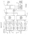
- FIG 3b we have shown the second stage of the baseband processing circuit of Figure 2.
- the second stage provides the timing and carrier recovery of the frame. As indicated, no overhead is allocated to clock and carrier training preambles. Instead, the baseband quadrature signal components are stored as sampled data in delay buffers while the clock and carrier phase are estimated. There are advantages if the entire slot is stored.
- a receiver assigned n slots per frame has an interval equal to the frame duration divided by n to process each slot. This can allow the signal processing circuit to operate with a lower clock rate which may be advantageous.
- the processing may be non-causal. Averaging can be done forwards and backwards.
- This stage is comprised of a first delay buffer 54 for storing the digitized samples received, a clock phase estimator 55 providing an estimate of the clock phase error to a data interpolation circuit 56.
- Delay buffer 57 provides additional time to process the time recovered samples at the carrier phase/gain estimator 58 which will provide a carrier phase/gain error estimate to correction circuit 59 the output of which is connected to a decision circuit 60.
- FIG 4 we have shown a block diagram of an implementation of the clock phase error estimator of Figure 3b.
- the clock is recovered using a Costas loop applied to the filtered baseband signals on one or both axes.
- This clock has a harmonic relationship to the baud rate fs/n where fs is the baud rate and n is greater than or equal to 1.
- Circuits 62 and 63 are used to process the sampled I and Q baseband signals by the reference clock signal 64 via divide-by-two circuits 65 and 66.
- the real and imaginary components x and y respectively for each axis are filtered by means of low pass filters 67, 68 and 69, 70 respectively.
- circuit 76 is a table look-up circuit implemented in a ROM in which the input is address information and the output is a set of coefficients for a finite impulse filter. These coefficients are used in circuit 56, the data interpolation circuit in an FIR (finite impulse response) filter to recover a sequence of I and Q samples with the correct clock phase.
- the start frame reference signal is used here to initiate the clock recovery process.
- the estimated clock phase error is used in conjunction with the clock interpolation circuit 56 shown in Figure 3b to interpolate the correctly timed data from the stored samples in delay buffer 54.
- the results are T/n-spaced sampled data for the I and Q axes where n is greater than or equal to 1.
- These samples are sent to a decision circuit 60, the output of which is the demodulated data.
- the demodulated data is also input to the frame detection circuit 61 which provides a start frame reference signal for the entire process.
- the decision circuit could be a simple threshold detector on the I and Q axes or an adaptive equalizer (decision feedback, Viterbi, etc.). It will be understood by those knowledgeable in this art that the input and output rates of the clock recovery circuit may or may not be the same.
- FIG. 5 is a block diagram of an implementation of the carrier phase and magnitude estimator of Figure 3b.
- the carrier measurement includes raising the I and Q baseband samples to the mth-power for m-PSK modulation at circuit 77 to account for four quadrant carrier phase ambiguity.
- the signals can then be converted at circuit 78 to provide a polar coordinate before being averaged at circuit 79, providing a carrier phase estimate 80 and a magnitude estimate 81. These are applied to circuit 59 of Figure 3b to restore symbols back to their proper locations. It will be understood to those knowledgeable in the art that a magnitude correction would not be required if an AGC circuit was used in this instance.
Landscapes
- Engineering & Computer Science (AREA)
- Computer Networks & Wireless Communication (AREA)
- Signal Processing (AREA)
- Digital Transmission Methods That Use Modulated Carrier Waves (AREA)
- Time-Division Multiplex Systems (AREA)
- Synchronisation In Digital Transmission Systems (AREA)
- Radio Relay Systems (AREA)
Applications Claiming Priority (2)
| Application Number | Priority Date | Filing Date | Title |
|---|---|---|---|
| CA574815 | 1988-08-15 | ||
| CA000574815A CA1288878C (fr) | 1988-08-15 | 1988-08-15 | Extraction sans sequence de synchronisation initiale du signal d'horloge etde la porteuse faisant partie d'un signal amrt |
Publications (3)
| Publication Number | Publication Date |
|---|---|
| EP0355587A2 true EP0355587A2 (fr) | 1990-02-28 |
| EP0355587A3 EP0355587A3 (fr) | 1991-11-27 |
| EP0355587B1 EP0355587B1 (fr) | 1995-11-08 |
Family
ID=4138553
Family Applications (1)
| Application Number | Title | Priority Date | Filing Date |
|---|---|---|---|
| EP89114740A Expired - Lifetime EP0355587B1 (fr) | 1988-08-15 | 1989-08-09 | Récupération d'horloge et de porteuse pour AMRT sans séquence de préambule |
Country Status (8)
| Country | Link |
|---|---|
| US (1) | US4977580A (fr) |
| EP (1) | EP0355587B1 (fr) |
| JP (1) | JPH0775359B2 (fr) |
| KR (1) | KR900004127A (fr) |
| AU (1) | AU610003B2 (fr) |
| BR (1) | BR8903752A (fr) |
| CA (1) | CA1288878C (fr) |
| DE (1) | DE68924739T2 (fr) |
Cited By (20)
| Publication number | Priority date | Publication date | Assignee | Title |
|---|---|---|---|---|
| EP0457542A3 (en) * | 1990-05-17 | 1993-03-03 | Sony Corporation | Transceiver with doppler correction |
| EP0486839A3 (en) * | 1990-10-25 | 1993-03-03 | Nec Corporation | Quasi-coherent mpsk demodulator |
| EP0533208A3 (en) * | 1991-09-19 | 1993-08-04 | Nec Corporation | Psk demodulator with feedback circuit for correcting phase and freqency errors |
| EP0535638A3 (en) * | 1991-09-30 | 1993-08-04 | Nec Corporation | Phase divider for complex signals |
| EP0533191A3 (en) * | 1991-09-19 | 1993-08-04 | Nec Corporation | Psk demodulator with freqency multiplication for the correction of phase and frequency errors |
| EP0554036A3 (en) * | 1992-01-27 | 1993-09-22 | Fujitsu Limited | Sampling clock generator for digital demodulator |
| EP0536687A3 (en) * | 1991-10-07 | 1993-11-03 | Nippon Telegraph & Telephone | Method and apparatus for demodulation with adaptive phase control in quasicoherent detection |
| EP0579100A1 (fr) * | 1992-07-14 | 1994-01-19 | Daimler-Benz Aerospace Aktiengesellschaft | Procédé et dispositif de correction de phase en bande de base dans un récepteur "PSK" |
| US5287067A (en) * | 1991-10-07 | 1994-02-15 | Nippon Telegraph And Telephone Corporation | Method and apparatus for demodulation with adaptive phase control in quasi-coherent detection |
| FR2706711A1 (fr) * | 1993-06-17 | 1994-12-23 | Matra Communication | Procédé et dispositif de démodulation de signal numérique. |
| AU663643B2 (en) * | 1993-03-25 | 1995-10-12 | Kabushiki Kaisha Toshiba | Digital communication apparatus including transmission error control |
| WO1996008926A1 (fr) * | 1994-09-16 | 1996-03-21 | Sony Corporation | Dispositif de sortie de donnees |
| WO1996008906A1 (fr) * | 1994-09-16 | 1996-03-21 | Ionica International Limited | Procede de demodulation et demodulateur |
| EP0912010A1 (fr) * | 1997-09-26 | 1999-04-28 | Micronas Intermetall GmbH | Boucle à verrouillage d'échantillonnage pour un récepteur de données transmis numériquement |
| EP0975126A1 (fr) * | 1998-07-23 | 2000-01-26 | STMicroelectronics S.A. | Procédé d'estimation d'erreur de fréquence d'un d'émodulateur QPSK |
| EP0763919A3 (fr) * | 1995-09-18 | 2000-08-09 | Mitsubishi Denki Kabushiki Kaisha | Démodulateur "QPSK" avec poursuite de fréquence et de phase |
| WO2000048334A1 (fr) * | 1999-02-08 | 2000-08-17 | Simoco International Limited | Acquisition de frequence et de base de temps dans un systeme de transmission radio |
| EP0924892A3 (fr) * | 1997-12-15 | 2003-12-10 | NEC Corporation | Circuit de récupération d'horloge et méthode de récupération d'horloge |
| EP1324529A3 (fr) * | 2001-12-28 | 2005-11-09 | Electronics and Telecommunications Research Institute | Méthode d'estimation d'horloge de symbole par une manière en avale |
| US7272175B2 (en) * | 2001-08-16 | 2007-09-18 | Dsp Group Inc. | Digital phase locked loop |
Families Citing this family (34)
| Publication number | Priority date | Publication date | Assignee | Title |
|---|---|---|---|---|
| US5638375A (en) * | 1988-11-30 | 1997-06-10 | Motorola, Inc. | AGC isolation of information in TDMA systems |
| SE462942B (sv) * | 1989-01-26 | 1990-09-17 | Ericsson Telefon Ab L M | Saett och anordning foer snabb frekvensstyrning av en koherent radiomottagare |
| IT1236978B (it) * | 1989-12-22 | 1993-05-12 | Italtel Spa | Metodo e dispositivo per la sincronizzazione tra una stazione radio fissa ed una stazione mobile in un sistema radiomobile digitale |
| JPH0494228A (ja) * | 1990-08-09 | 1992-03-26 | Matsushita Electric Ind Co Ltd | ダイナミックチャネル割当方法 |
| US5123033A (en) * | 1990-09-27 | 1992-06-16 | At&T Bell Laboratories | Extraction of an exact symbol rate as applied to bandwidth compression of modem signals through demodulation and remodulation |
| GB2256993B (en) * | 1990-12-17 | 1995-06-21 | Motorola Inc | Frequency and time slot synchronization using adaptive filtering |
| US5241688A (en) * | 1990-12-17 | 1993-08-31 | Motorola, Inc. | Frequency and time slot synchronizaton using adaptive filtering |
| IT1244206B (it) * | 1990-12-19 | 1994-07-08 | Telettra Spa | Sistema e circuito per la stima della frequenza di portante di un segnale |
| US5214674A (en) * | 1991-01-25 | 1993-05-25 | Comsat | Method and apparatus for carrier synchronization acquisition in a digital burst mode communication system |
| FI89431C (fi) * | 1991-05-14 | 1993-09-27 | Nokia Mobile Phones Ltd | Grovinstaellning av kanalfrekvensen |
| FR2682841B1 (fr) * | 1991-10-21 | 1993-11-19 | Alcatel Telspace | Procede de detection de faux accrochages d'un signal de reference sur un signal initialement module en modulation numerique plurivalente decalee, procede de demodulation numerique coherente l'utilisant. |
| US5390216A (en) * | 1991-11-02 | 1995-02-14 | Robert Bosch Gmbh | Synchronization method for a mobile radiotelephone |
| JP3255179B2 (ja) * | 1992-02-14 | 2002-02-12 | ソニー株式会社 | データ検出装置 |
| JP2888398B2 (ja) * | 1992-12-10 | 1999-05-10 | 株式会社日立製作所 | ディジタル情報再生装置 |
| US5652541A (en) * | 1993-11-23 | 1997-07-29 | Motorola, Inc. | Data demodulator employing decision feedback for reference parameter recovery and method used therin |
| US5497400A (en) * | 1993-12-06 | 1996-03-05 | Motorola, Inc. | Decision feedback demodulator with phase and frequency estimation |
| SE502168C2 (sv) * | 1993-12-29 | 1995-09-04 | Ericsson Telefon Ab L M | Förfarande och anordning vid ett radiokommunikationssystem |
| US5533063A (en) * | 1994-01-31 | 1996-07-02 | The Regents Of The University Of California | Method and apparatus for multipath channel shaping |
| US5590140A (en) * | 1994-12-30 | 1996-12-31 | Lucent Technologies Inc. | Clock recovery extrapolation |
| US5799034A (en) * | 1995-12-06 | 1998-08-25 | Rockwell International Corporation | Frequency acquisition method for direct sequence spread spectrum systems |
| US5751718A (en) * | 1996-02-20 | 1998-05-12 | Motorola, Inc. | Simultaneous transfer of voice and data information using multi-rate vocoder and byte control protocol |
| US5889827A (en) * | 1996-12-12 | 1999-03-30 | Ericsson Inc. | Method and apparatus for digital symbol detection using medium response estimates |
| US6735416B1 (en) * | 1999-05-25 | 2004-05-11 | Xm Satellite Radio, Inc. | Receiver architecture for SDARS full band signal reception having an analog conversion to baseband stage |
| KR100669403B1 (ko) * | 2000-05-04 | 2007-01-15 | 삼성전자주식회사 | 브이에스비/큐에이엠 공용 수신기 및 수신방법 |
| DE10058766A1 (de) * | 2000-11-27 | 2002-06-13 | Trend Network Ag | Verfahren zur unidirektionalen Datenübertragung, insbesondere über die Stromzufuhr eines Fahrzeuges |
| US7428278B2 (en) * | 2002-05-09 | 2008-09-23 | Interdigital Technology Corporation | Method and apparatus for parallel midamble cancellation |
| US7079614B2 (en) * | 2002-11-21 | 2006-07-18 | Agilent Technologies, Inc. | Method of generating a measure of a mistiming and apparatus therefor |
| DE102004047424A1 (de) * | 2004-09-28 | 2006-04-06 | Micronas Gmbh | Schaltung und Verfahren zur Trägerrückgewinnung |
| DE102004048572A1 (de) * | 2004-10-04 | 2006-04-13 | Micronas Gmbh | Verfahren sowie Schaltungsanordnung zur Unterdrückung einer orthogonalen Störung |
| DE102004054893A1 (de) * | 2004-11-12 | 2006-05-24 | Micronas Gmbh | Verfahren und Schaltungsanordnung zur Kanalfilterung analog oder digital modulierter TV-Signale |
| US8139700B2 (en) * | 2009-06-26 | 2012-03-20 | International Business Machines Corporation | Dynamic quadrature clock correction for a phase rotator system |
| US8289061B2 (en) * | 2009-09-29 | 2012-10-16 | Integrated Device Technology, Inc. | Technique to reduce clock recovery amplitude modulation in high-speed serial transceiver |
| US9137006B1 (en) * | 2014-10-22 | 2015-09-15 | The United States Of America As Represented By The Secretary Of The Air Force | Non-integer oversampled timing recovery for higher order quadrature modulation communication systems using quadrature and in-phase samples |
| CN111610752B (zh) * | 2020-05-24 | 2021-07-27 | 西安交通大学 | 一种基于伺服进给系统衰放倍率的插补指令评价方法 |
Family Cites Families (5)
| Publication number | Priority date | Publication date | Assignee | Title |
|---|---|---|---|---|
| US3792364A (en) * | 1972-08-03 | 1974-02-12 | Sangamo Electric Co | Method and apparatus for detecting absolute value amplitude of am suppressed carrier signals |
| US4631489A (en) | 1985-07-05 | 1986-12-23 | Motorola, Inc. | FM signal magnitude quantizer and demodulator compatible with digital signal processing |
| US4794341A (en) * | 1985-11-05 | 1988-12-27 | Signal Processors Limited | Digital filters and demodulators |
| US4852090A (en) * | 1987-02-02 | 1989-07-25 | Motorola, Inc. | TDMA communications system with adaptive equalization |
| US4866739A (en) * | 1988-02-22 | 1989-09-12 | Silicon Systems, Inc. | Digital fast recovery timing algorithm |
-
1988
- 1988-08-15 CA CA000574815A patent/CA1288878C/fr not_active Expired - Lifetime
- 1988-10-13 US US07/256,958 patent/US4977580A/en not_active Expired - Lifetime
-
1989
- 1989-07-06 AU AU37938/89A patent/AU610003B2/en not_active Ceased
- 1989-07-27 BR BR898903752A patent/BR8903752A/pt unknown
- 1989-08-08 JP JP1204020A patent/JPH0775359B2/ja not_active Expired - Fee Related
- 1989-08-09 DE DE68924739T patent/DE68924739T2/de not_active Expired - Fee Related
- 1989-08-09 EP EP89114740A patent/EP0355587B1/fr not_active Expired - Lifetime
- 1989-08-14 KR KR1019890011583A patent/KR900004127A/ko not_active Withdrawn
Cited By (28)
| Publication number | Priority date | Publication date | Assignee | Title |
|---|---|---|---|---|
| US5261120A (en) * | 1990-05-17 | 1993-11-09 | Sony Corporation | Method and apparatus for transmitting a signal with an offset which follows a received signal |
| EP0457542A3 (en) * | 1990-05-17 | 1993-03-03 | Sony Corporation | Transceiver with doppler correction |
| EP0486839A3 (en) * | 1990-10-25 | 1993-03-03 | Nec Corporation | Quasi-coherent mpsk demodulator |
| EP0533208A3 (en) * | 1991-09-19 | 1993-08-04 | Nec Corporation | Psk demodulator with feedback circuit for correcting phase and freqency errors |
| EP0533191A3 (en) * | 1991-09-19 | 1993-08-04 | Nec Corporation | Psk demodulator with freqency multiplication for the correction of phase and frequency errors |
| EP0535638A3 (en) * | 1991-09-30 | 1993-08-04 | Nec Corporation | Phase divider for complex signals |
| EP0536687A3 (en) * | 1991-10-07 | 1993-11-03 | Nippon Telegraph & Telephone | Method and apparatus for demodulation with adaptive phase control in quasicoherent detection |
| US5287067A (en) * | 1991-10-07 | 1994-02-15 | Nippon Telegraph And Telephone Corporation | Method and apparatus for demodulation with adaptive phase control in quasi-coherent detection |
| US5442656A (en) * | 1992-01-27 | 1995-08-15 | Fujitsu Limited | Timing extraction device and data transmission device using the timing extraction device |
| EP0554036A3 (en) * | 1992-01-27 | 1993-09-22 | Fujitsu Limited | Sampling clock generator for digital demodulator |
| EP0579100A1 (fr) * | 1992-07-14 | 1994-01-19 | Daimler-Benz Aerospace Aktiengesellschaft | Procédé et dispositif de correction de phase en bande de base dans un récepteur "PSK" |
| AU663643B2 (en) * | 1993-03-25 | 1995-10-12 | Kabushiki Kaisha Toshiba | Digital communication apparatus including transmission error control |
| US5640125A (en) * | 1993-06-17 | 1997-06-17 | Matra Communication | Digital PSK-type demodulator having clock recovery before carrier recovery |
| FR2706711A1 (fr) * | 1993-06-17 | 1994-12-23 | Matra Communication | Procédé et dispositif de démodulation de signal numérique. |
| WO1995001034A1 (fr) * | 1993-06-17 | 1995-01-05 | Matra Communication | Procede et dispositif de demodulation de signal numerique |
| WO1996008926A1 (fr) * | 1994-09-16 | 1996-03-21 | Sony Corporation | Dispositif de sortie de donnees |
| WO1996008906A1 (fr) * | 1994-09-16 | 1996-03-21 | Ionica International Limited | Procede de demodulation et demodulateur |
| EP0763919A3 (fr) * | 1995-09-18 | 2000-08-09 | Mitsubishi Denki Kabushiki Kaisha | Démodulateur "QPSK" avec poursuite de fréquence et de phase |
| EP0912010A1 (fr) * | 1997-09-26 | 1999-04-28 | Micronas Intermetall GmbH | Boucle à verrouillage d'échantillonnage pour un récepteur de données transmis numériquement |
| EP0924892A3 (fr) * | 1997-12-15 | 2003-12-10 | NEC Corporation | Circuit de récupération d'horloge et méthode de récupération d'horloge |
| EP0975126A1 (fr) * | 1998-07-23 | 2000-01-26 | STMicroelectronics S.A. | Procédé d'estimation d'erreur de fréquence d'un d'émodulateur QPSK |
| FR2781626A1 (fr) * | 1998-07-23 | 2000-01-28 | St Microelectronics Sa | Procede d'estimation d'erreur de frequence d'un demodulateur qpsk |
| US6570936B1 (en) | 1998-07-23 | 2003-05-27 | Stmicroelectronics S.A. | Frequency error estimation method and system for a QPSK demodulator |
| WO2000048334A1 (fr) * | 1999-02-08 | 2000-08-17 | Simoco International Limited | Acquisition de frequence et de base de temps dans un systeme de transmission radio |
| US7272175B2 (en) * | 2001-08-16 | 2007-09-18 | Dsp Group Inc. | Digital phase locked loop |
| US7738600B2 (en) | 2001-08-16 | 2010-06-15 | Dsp Group Inc. | Digital phase locked loop |
| EP1324529A3 (fr) * | 2001-12-28 | 2005-11-09 | Electronics and Telecommunications Research Institute | Méthode d'estimation d'horloge de symbole par une manière en avale |
| US7092467B2 (en) | 2001-12-28 | 2006-08-15 | Electronics And Telecommunications Research Institute | Method for estimating symbol timing in feed-forward manner |
Also Published As
| Publication number | Publication date |
|---|---|
| US4977580A (en) | 1990-12-11 |
| DE68924739D1 (de) | 1995-12-14 |
| BR8903752A (pt) | 1990-03-20 |
| CA1288878C (fr) | 1991-09-10 |
| AU610003B2 (en) | 1991-05-09 |
| EP0355587B1 (fr) | 1995-11-08 |
| EP0355587A3 (fr) | 1991-11-27 |
| KR900004127A (ko) | 1990-03-27 |
| DE68924739T2 (de) | 1996-04-11 |
| JPH0775359B2 (ja) | 1995-08-09 |
| AU3793889A (en) | 1990-02-15 |
| JPH02101845A (ja) | 1990-04-13 |
Similar Documents
| Publication | Publication Date | Title |
|---|---|---|
| US4977580A (en) | Timing and carrier recovery in TDMA without preamble sequence | |
| US5594758A (en) | Frequency controller and method of correcting phase estimates in a PSK demodulator using frequency control | |
| US7099421B2 (en) | Synchronization signal detector and method | |
| US4764940A (en) | Modem for RF subscriber telephone system | |
| US20100075611A1 (en) | Apparatus and method for improved wireless communication reliability and performance in process control systems | |
| EP3706380B1 (fr) | Détecteur d'erreur de modulation par déplacement de fréquence (fsk) et procédé associé | |
| JP2002026775A (ja) | 無線受信装置における周波数オフセットを減少させる方法および装置 | |
| EP0751644B1 (fr) | Méthode de détection de signal de commande avec calibration d'erreurs et unité d'abonneé pour ce faire | |
| US5200977A (en) | Terminal unit apparatus for time division multiplexing access communications system | |
| US7167535B2 (en) | Circuit sharing for frequency and phase error correction | |
| EP0958686B1 (fr) | Demodulation a branches phase et amplitude distinctes | |
| JP2959498B2 (ja) | 自動周波数制御回路 | |
| JP3183266B2 (ja) | 自動周波数制御回路 | |
| KR100245330B1 (ko) | 디지털 통신 시스템의 위상 및 주파수 검출 장치 | |
| Kobayashi et al. | Fully digital burst modem for satellite multimedia communication systems | |
| US6243429B1 (en) | Data demodulator for correcting bit errors | |
| JP4139814B2 (ja) | 周波数誤差検出方法、受信方法、及び送受信方法 | |
| JP2706481B2 (ja) | データ伝送装置 | |
| JP2002344552A (ja) | プリアンブル長推定回路、復調装置、および通信システム | |
| CN1206521A (zh) | Tdma方法,发射机和接收机 | |
| JP2001186117A (ja) | フレームタイミング捕捉方法および装置ならびにtdma復調装置 | |
| JP2000504193A (ja) | Tdma方法、およびその送信機と受信機 |
Legal Events
| Date | Code | Title | Description |
|---|---|---|---|
| PUAI | Public reference made under article 153(3) epc to a published international application that has entered the european phase |
Free format text: ORIGINAL CODE: 0009012 |
|
| AK | Designated contracting states |
Kind code of ref document: A2 Designated state(s): DE FR GB IT NL SE |
|
| PUAL | Search report despatched |
Free format text: ORIGINAL CODE: 0009013 |
|
| AK | Designated contracting states |
Kind code of ref document: A3 Designated state(s): DE FR GB IT NL SE |
|
| 17P | Request for examination filed |
Effective date: 19920128 |
|
| 17Q | First examination report despatched |
Effective date: 19931105 |
|
| GRAA | (expected) grant |
Free format text: ORIGINAL CODE: 0009210 |
|
| AK | Designated contracting states |
Kind code of ref document: B1 Designated state(s): DE FR GB IT NL SE |
|
| PG25 | Lapsed in a contracting state [announced via postgrant information from national office to epo] |
Ref country code: IT Free format text: LAPSE BECAUSE OF FAILURE TO SUBMIT A TRANSLATION OF THE DESCRIPTION OR TO PAY THE FEE WITHIN THE PRE;WARNING: LAPSES OF ITALIAN PATENTS WITH EFFECTIVE DATE BEFORE 2007 MAY HAVE OCCURRED AT ANY TIME BEFORE 2007. THE CORRECT EFFECTIVE DATE MAY BE DIFFERENT FROM THE ONE RECORDED.SCRIBED TIME-LIMIT Effective date: 19951108 Ref country code: NL Free format text: LAPSE BECAUSE OF FAILURE TO SUBMIT A TRANSLATION OF THE DESCRIPTION OR TO PAY THE FEE WITHIN THE PRESCRIBED TIME-LIMIT Effective date: 19951108 |
|
| REF | Corresponds to: |
Ref document number: 68924739 Country of ref document: DE Date of ref document: 19951214 |
|
| ET | Fr: translation filed | ||
| PG25 | Lapsed in a contracting state [announced via postgrant information from national office to epo] |
Ref country code: SE Effective date: 19960208 |
|
| NLV1 | Nl: lapsed or annulled due to failure to fulfill the requirements of art. 29p and 29m of the patents act | ||
| PLBE | No opposition filed within time limit |
Free format text: ORIGINAL CODE: 0009261 |
|
| STAA | Information on the status of an ep patent application or granted ep patent |
Free format text: STATUS: NO OPPOSITION FILED WITHIN TIME LIMIT |
|
| 26N | No opposition filed | ||
| PGFP | Annual fee paid to national office [announced via postgrant information from national office to epo] |
Ref country code: GB Payment date: 19990716 Year of fee payment: 11 |
|
| PG25 | Lapsed in a contracting state [announced via postgrant information from national office to epo] |
Ref country code: GB Free format text: LAPSE BECAUSE OF NON-PAYMENT OF DUE FEES Effective date: 20000809 |
|
| GBPC | Gb: european patent ceased through non-payment of renewal fee |
Effective date: 20000809 |
|
| REG | Reference to a national code |
Ref country code: FR Ref legal event code: CD |
|
| PGFP | Annual fee paid to national office [announced via postgrant information from national office to epo] |
Ref country code: DE Payment date: 20040831 Year of fee payment: 16 |
|
| PG25 | Lapsed in a contracting state [announced via postgrant information from national office to epo] |
Ref country code: DE Free format text: LAPSE BECAUSE OF NON-PAYMENT OF DUE FEES Effective date: 20060301 |
|
| PGFP | Annual fee paid to national office [announced via postgrant information from national office to epo] |
Ref country code: FR Payment date: 20060803 Year of fee payment: 18 |
|
| REG | Reference to a national code |
Ref country code: FR Ref legal event code: ST Effective date: 20080430 |
|
| PG25 | Lapsed in a contracting state [announced via postgrant information from national office to epo] |
Ref country code: FR Free format text: LAPSE BECAUSE OF NON-PAYMENT OF DUE FEES Effective date: 20070831 |