EP0355769A2 - Circuit fournissant un signal d'horloge - Google Patents
Circuit fournissant un signal d'horloge Download PDFInfo
- Publication number
- EP0355769A2 EP0355769A2 EP89115381A EP89115381A EP0355769A2 EP 0355769 A2 EP0355769 A2 EP 0355769A2 EP 89115381 A EP89115381 A EP 89115381A EP 89115381 A EP89115381 A EP 89115381A EP 0355769 A2 EP0355769 A2 EP 0355769A2
- Authority
- EP
- European Patent Office
- Prior art keywords
- buffer
- phase
- line
- supply circuit
- clock
- Prior art date
- Legal status (The legal status is an assumption and is not a legal conclusion. Google has not performed a legal analysis and makes no representation as to the accuracy of the status listed.)
- Granted
Links
Images


Classifications
-
- H—ELECTRICITY
- H03—ELECTRONIC CIRCUITRY
- H03K—PULSE TECHNIQUE
- H03K3/00—Circuits for generating electric pulses; Monostable, bistable or multistable circuits
-
- G—PHYSICS
- G06—COMPUTING OR CALCULATING; COUNTING
- G06F—ELECTRIC DIGITAL DATA PROCESSING
- G06F1/00—Details not covered by groups G06F3/00 - G06F13/00 and G06F21/00
- G06F1/04—Generating or distributing clock signals or signals derived directly therefrom
- G06F1/10—Distribution of clock signals, e.g. skew
Definitions
- the present invention relates to a clock supply circuit, and more particularly to a clock supply circuit having a function which can control an inner clock skew.
- the delay between the Q output and the D input of the two F/F is controlled larger than the clock skew.
- the operation speed of the LSI becomes slower. Accordingly, it is required to control the clock skew as small as possible.
- Fig. 1 shows an example of a centralized, system which is also a clock drive system of a group of F/Fs according to the prior art.
- means flip-flop and BU means clock buffer or buffer.
- Each the F/F is so connected to a buffer (BU) 1 and a buffer (BU) 2 as to construct a branch structure.
- the outer clock is inputted into the buffer 1 first, then inputted into the buffer 2, thereafter transmitted into each F/F from the buffer 2.
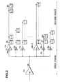
- Fig. 2 shows an example of a distributed drive system which is another clock drive system according to the prior art.
- F/F means flip-flop and BU 1a , BU 2a , ..., BU Na-1 , and BU Na (N is a natural number of 1 or more) mean buffer.
- Each F/F is connected in series to each of the BU 2a , BU 3a , ..., and BU N3 .
- the buffers are composed in two phases.
- the buffer 1a in a first phase drives the buffers 2a, ..., to Na (N is a natural number of 2 or more) in a second phase, and also drives each of the F/Fs which are dependent on each buffer.
- drive ability ⁇ 2 and ⁇ Na-1 of the buffer 2a and the buffer Na-1 which respectively have different numbers of F/Fs are determined in the following manner.
- the linear length from a point 1A to a point 1B is different that from the point 1A to a point 1D. Accordingly, a clock delay caused by RC delay on the line occurs, and a clock skew corresponding thereto also occurs. Namely, the clock skew can not be avoided by the drive system in principle. Particularly, when the scale of the LSI is large, the magnitude of the clock skew can not be ignored. Moreover, since the system is a collective drive system, it is necessary for the buffer 2 to have a big drive ability to operate a plurality of F/Fs. Accordingly, a large amount of current should flow locally in the buffer, thus noise and wrong operation are likely to be caused.
- a clock supply circuit comprises a first phase which includes a first buffer and at least one line from a predetermined point on the output side of the first buffer to an input point of each second buffer in each channel and a dependent phase which is composed of each second buffer and a group of flip-flops which is dependent thereon, and the circuit is so constructed as to uniformalize line length and capacitive load or F/F in each phase, to unify drive ability of the buffers in the dependent phase, and adjust load capacity by providing extra capacities for adjustment of a clock skew.
- uniformalized load can be driven by the buffers having the same drive ability , so that the clock skew can be reduced.
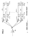
- Fig. 3 shows a first embodiment of a clock supply circuit according to the present invention.
- CH N N is a natural number
- CH N means channel.
- each line length, and each line width from a point 3A on the output side of a buffer (BU) 10 to each of buffers 11 ⁇ 1, 11 ⁇ 2, ..., 11- (N-1) , to 11 -N (N is a natural number) in a first phase are respectively constructed to be the same.
- Fig. 4 shows a second embodiment of a clock supply circuit according to the present invention.
- a line condition in a first phase is the same as the embodiment which was described in Fig. 3. While, the number of F/F of each channel (CH N ) and each linear length for connecting these in a second phase are respectively different. Namely, the line conditions from a point 4A on the output side of a buffer 10 to points 4C, 4D, ..., 4F, and 4G which are respectively input points of buffers 11 ⁇ 1, 11 ⁇ 2, and 11 ⁇ 3, ..., 11 -N dispersed into the respective channels in the first phase are the same. For example, in the second phase of the same drawing, a channel CH1 has the largest number of F/Fs in these channels.
- Each of the load capacities has an adjusted value in accordance with the number of F/Fs which are connected to each of the buffer 11 ⁇ 2, 11 ⁇ 3, ..., and 11 -N in each of the channels CH2, CH3, ..., and CH N , furthermore it is so adjusted as to be substantially the same delay as a signal delay in the standard channel CH1 in consideration of the linear length of the respective channels CH2, CH3, ..., and CH N .
- the load capacity C N is calculated by the following equation:
- C N Difference in the stray capacity of the line to the standard channel + a gate capacity corresponding to the number of F/Fs which is less than the standard channel.
- Fig. 5 shows a third embodiment of a clock supply circuit according to the present invention.
- the construction of a second phase is the same as that of the embodiment in Fig. 4, and the determination manner of the values of the capacities for the respective adjustments is also the same as that of the embodiment in Fig. 4, thus the detailed description on the matter will be omitted herein.
- input line lengths from a point 5A on the output side of a first buffer 10 each of points 5C, 5D, ..., 5F, and 5G which are respectively input points of buffers 11 ⁇ 1, 11 ⁇ 2, ..., 11 -(N-1) , and 11 -N in a first phase are different from one another.
- adjustment capacities C12, C13, ..., and C 1N for prevention of the clock skew caused by the RC delay of the input lines having different lengths on the basis of a specific buffer having a longest input line, for example, the buffer 11 ⁇ 1 in the same drawing.
- each value of the respective adjustment capacities can be determined in accordance with the respective shortages of capacity in the input lines.
- the construction thereof is divided into the first phase which includes the lines from the first buffer to the input points of the respective buffer which belong to the respective channels in the next phase, and the second phase comprises the respective buffers and the respective channels including the F/Fs which are connected to thereon, and the F/Fs as the load are driven in the substantially uniformalized state of line conditions in the respective phases. Therefore, the clock skew can be controlled to be small.
- the respective buffers in the respective channels in the second phase may be the same kind, and may have the same performance or the same drive ability, it becomes easy to design the circuit.
- the adjustment can be easily achieved by adding adjustable capacities so as to adjust the states of the circuit of the respective channels or the line conditions thereof into substantially uniform.
- the clock skew can be controlled to be uniform and small even when the drive ability of the respective buffers in the respective channels fluctuate a little.
Landscapes
- Engineering & Computer Science (AREA)
- Theoretical Computer Science (AREA)
- Physics & Mathematics (AREA)
- General Engineering & Computer Science (AREA)
- General Physics & Mathematics (AREA)
- Semiconductor Integrated Circuits (AREA)
- Design And Manufacture Of Integrated Circuits (AREA)
- Manipulation Of Pulses (AREA)
- Dram (AREA)
Applications Claiming Priority (2)
| Application Number | Priority Date | Filing Date | Title |
|---|---|---|---|
| JP63205868A JPH0736422B2 (ja) | 1988-08-19 | 1988-08-19 | クロック供給回路 |
| JP205868/88 | 1988-08-19 |
Publications (3)
| Publication Number | Publication Date |
|---|---|
| EP0355769A2 true EP0355769A2 (fr) | 1990-02-28 |
| EP0355769A3 EP0355769A3 (en) | 1990-06-06 |
| EP0355769B1 EP0355769B1 (fr) | 1995-11-15 |
Family
ID=16514055
Family Applications (1)
| Application Number | Title | Priority Date | Filing Date |
|---|---|---|---|
| EP89115381A Expired - Lifetime EP0355769B1 (fr) | 1988-08-19 | 1989-08-21 | Circuit fournissant un signal d'horloge |
Country Status (5)
| Country | Link |
|---|---|
| US (1) | US5013942A (fr) |
| EP (1) | EP0355769B1 (fr) |
| JP (1) | JPH0736422B2 (fr) |
| KR (1) | KR920010208B1 (fr) |
| DE (1) | DE68924811T2 (fr) |
Cited By (2)
| Publication number | Priority date | Publication date | Assignee | Title |
|---|---|---|---|---|
| EP0451079A3 (en) * | 1990-03-30 | 1992-03-25 | International Business Machines Corporation | Reducing clock skew in large-scale integrated circuits |
| CN112257375A (zh) * | 2020-10-26 | 2021-01-22 | 海光信息技术股份有限公司 | 用于集成电路设计的布局调整方法、装置和电子设备 |
Families Citing this family (29)
| Publication number | Priority date | Publication date | Assignee | Title |
|---|---|---|---|---|
| US5239215A (en) * | 1988-05-16 | 1993-08-24 | Matsushita Electric Industrial Co., Ltd. | Large scale integrated circuit configured to eliminate clock signal skew effects |
| JPH02127813A (ja) * | 1988-11-08 | 1990-05-16 | Matsushita Electron Corp | 半導体集積回路 |
| JPH0824143B2 (ja) * | 1989-02-08 | 1996-03-06 | 株式会社東芝 | 集積回路の配置配線方式 |
| JP3030991B2 (ja) * | 1991-11-14 | 2000-04-10 | 日本電気株式会社 | 半導体集積回路 |
| JP3006739B2 (ja) * | 1992-04-20 | 2000-02-07 | 松下電器産業株式会社 | 半導体集積回路装置 |
| US5396129A (en) * | 1992-05-25 | 1995-03-07 | Matsushita Electronics Corporation | Semiconductor integrated circuit apparatus comprising clock signal line formed in a ring shape |
| JP3048471B2 (ja) * | 1992-09-08 | 2000-06-05 | 沖電気工業株式会社 | クロック供給回路及びクロックスキュー調整方法 |
| US5444407A (en) * | 1992-12-28 | 1995-08-22 | Advanced Micro Devices, Inc. | Microprocessor with distributed clock generators |
| ES2113498T3 (es) * | 1992-12-28 | 1998-05-01 | Advanced Micro Devices Inc | Circuito de microprocesador con dos señales de temporizacion. |
| KR100293596B1 (ko) * | 1993-01-27 | 2001-09-17 | 가나이 쓰도무 | Lsi내클럭분배회로 |
| US5444406A (en) * | 1993-02-08 | 1995-08-22 | Advanced Micro Devices, Inc. | Self-adjusting variable drive strength buffer circuit and method for controlling the drive strength of a buffer circuit |
| US5467033A (en) * | 1993-07-02 | 1995-11-14 | Tandem Computers Incorporated | Chip clock skew control method and apparatus |
| US5481209A (en) * | 1993-09-20 | 1996-01-02 | Lsi Logic Corporation | Clock distribution and control in an integrated circuit |
| US5652529A (en) * | 1995-06-02 | 1997-07-29 | International Business Machines Corporation | Programmable array clock/reset resource |
| US5705942A (en) * | 1995-09-29 | 1998-01-06 | Intel Corporation | Method and apparatus for locating and improving critical speed paths in VLSI integrated circuits |
| US5818263A (en) * | 1995-09-29 | 1998-10-06 | Intel Corporation | Method and apparatus for locating and improving race conditions in VLSI integrated circuits |
| US5742832A (en) * | 1996-02-09 | 1998-04-21 | Advanced Micro Devices | Computer system with programmable driver output's strengths responsive to control signal matching preassigned address range |
| JP2778572B2 (ja) * | 1996-03-21 | 1998-07-23 | 日本電気株式会社 | クロック分配回路 |
| US5717229A (en) * | 1996-03-26 | 1998-02-10 | Intel Corporation | Method and apparatus for routing a clock tree in an integrated circuit package |
| US5790841A (en) * | 1996-04-15 | 1998-08-04 | Advanced Micro Devices, Inc. | Method for placement of clock buffers in a clock distribution system |
| US6211703B1 (en) * | 1996-06-07 | 2001-04-03 | Hitachi, Ltd. | Signal transmission system |
| US5892373A (en) * | 1997-01-29 | 1999-04-06 | Advanced Micro Devices, Inc. | Distributed gated clock driver |
| US6380787B1 (en) * | 1999-08-31 | 2002-04-30 | Micron Technology, Inc. | Integrated circuit and method for minimizing clock skews |
| JP4618839B2 (ja) * | 2000-01-24 | 2011-01-26 | ルネサスエレクトロニクス株式会社 | 半導体記憶装置 |
| TW494293B (en) * | 2000-12-22 | 2002-07-11 | Faraday Tech Corp | Clock signal network structure |
| TW560128B (en) * | 2002-08-09 | 2003-11-01 | Via Tech Inc | Method and related circuitry for buffering output signals of a chip with even number driving circuits |
| US7639037B1 (en) * | 2008-06-27 | 2009-12-29 | Sun Microsystems, Inc. | Method and system for sizing flow control buffers |
| US8183890B1 (en) | 2008-09-10 | 2012-05-22 | Marvell International Ltd. | Method and apparatus for sampling |
| US11095272B2 (en) * | 2018-09-21 | 2021-08-17 | Taiwan Semiconductor Manufacturing Company, Ltd. | Flip-flop cell |
Family Cites Families (11)
| Publication number | Priority date | Publication date | Assignee | Title |
|---|---|---|---|---|
| JPS55115352A (en) * | 1979-02-27 | 1980-09-05 | Fujitsu Ltd | Clock distributing circuit of ic device |
| US4639615A (en) * | 1983-12-28 | 1987-01-27 | At&T Bell Laboratories | Trimmable loading elements to control clock skew |
| US4692633A (en) * | 1984-07-02 | 1987-09-08 | International Business Machines Corporation | Edge sensitive single clock latch apparatus with a skew compensated scan function |
| JPS6182525A (ja) * | 1984-09-29 | 1986-04-26 | Toshiba Corp | 半導体集積回路装置 |
| JPS61146951U (fr) * | 1985-03-04 | 1986-09-10 | ||
| US4769558A (en) * | 1986-07-09 | 1988-09-06 | Eta Systems, Inc. | Integrated circuit clock bus layout delay system |
| JPS6387744A (ja) * | 1986-09-30 | 1988-04-19 | Nec Corp | 半導体集積回路 |
| JPH083773B2 (ja) * | 1987-02-23 | 1996-01-17 | 株式会社日立製作所 | 大規模半導体論理回路 |
| JP2690083B2 (ja) * | 1987-07-22 | 1997-12-10 | 株式会社日立製作所 | 半導体集積回路装置 |
| JPH0815210B2 (ja) * | 1987-06-04 | 1996-02-14 | 日本電気株式会社 | マスタスライス方式集積回路 |
| US4868425A (en) * | 1987-12-07 | 1989-09-19 | Vtc Incorporated | Skew compensated RS422 buffer |
-
1988
- 1988-08-19 JP JP63205868A patent/JPH0736422B2/ja not_active Expired - Fee Related
-
1989
- 1989-08-17 US US07/394,803 patent/US5013942A/en not_active Expired - Lifetime
- 1989-08-18 KR KR1019890011766A patent/KR920010208B1/ko not_active Expired
- 1989-08-21 DE DE68924811T patent/DE68924811T2/de not_active Expired - Fee Related
- 1989-08-21 EP EP89115381A patent/EP0355769B1/fr not_active Expired - Lifetime
Cited By (3)
| Publication number | Priority date | Publication date | Assignee | Title |
|---|---|---|---|---|
| EP0451079A3 (en) * | 1990-03-30 | 1992-03-25 | International Business Machines Corporation | Reducing clock skew in large-scale integrated circuits |
| CN112257375A (zh) * | 2020-10-26 | 2021-01-22 | 海光信息技术股份有限公司 | 用于集成电路设计的布局调整方法、装置和电子设备 |
| CN112257375B (zh) * | 2020-10-26 | 2023-10-10 | 海光信息技术(苏州)有限公司 | 用于集成电路设计的布局调整方法、装置和电子设备 |
Also Published As
| Publication number | Publication date |
|---|---|
| US5013942A (en) | 1991-05-07 |
| JPH0254950A (ja) | 1990-02-23 |
| DE68924811D1 (de) | 1995-12-21 |
| EP0355769A3 (en) | 1990-06-06 |
| KR900004103A (ko) | 1990-03-27 |
| JPH0736422B2 (ja) | 1995-04-19 |
| KR920010208B1 (ko) | 1992-11-21 |
| EP0355769B1 (fr) | 1995-11-15 |
| DE68924811T2 (de) | 1996-05-30 |
Similar Documents
| Publication | Publication Date | Title |
|---|---|---|
| EP0355769A2 (fr) | Circuit fournissant un signal d'horloge | |
| JP2717111B2 (ja) | 送信ゲート直列マルチプレクサ | |
| JP2650113B2 (ja) | 集積回路チツプとその動作速度検出方法 | |
| US5208491A (en) | Field programmable gate array | |
| KR900008023B1 (ko) | 대규모 반도체 논리장치 | |
| US6867632B2 (en) | Semiconductor integrated circuit device | |
| US6239646B1 (en) | High-speed, multiple-input multiplexer scheme | |
| US4866310A (en) | Clock signal generator | |
| GB2108344A (en) | Improvements in or relating to fet circuits | |
| US4593205A (en) | Macrocell array having an on-chip clock generator | |
| EP0111262A2 (fr) | Multiplexeur de sortie avec un retard équivalent à celui d'une porte | |
| KR100209224B1 (ko) | 고속 다중화기 | |
| JPH077808B2 (ja) | 集積回路 | |
| US3548319A (en) | Synchronous digital counter | |
| US5151868A (en) | Signal line terminal allocation method | |
| EP0115004A1 (fr) | Circuit de compteur asynchrone à temps réduit de propagation | |
| US5880607A (en) | Clock distribution network with modular buffers | |
| EP0380095B1 (fr) | Circuit logique | |
| US4821299A (en) | Semiconductor integrated circuit device including shift register having substantially equalized wiring between stages thereof | |
| US6198305B1 (en) | Reduced area product-term array | |
| US6369670B1 (en) | Dynamically adjustable tapped delay line | |
| KR100221415B1 (ko) | 신호처리장치 | |
| US5557581A (en) | Logic and memory circuit with reduced input-to-output signal propagation delay | |
| EP0105520B1 (fr) | Circuits détecteurs de transition et circuits intégrés MOS utilisés avec un tel détecteur | |
| US5307352A (en) | Switch matrix multiplexers |
Legal Events
| Date | Code | Title | Description |
|---|---|---|---|
| PUAI | Public reference made under article 153(3) epc to a published international application that has entered the european phase |
Free format text: ORIGINAL CODE: 0009012 |
|
| 17P | Request for examination filed |
Effective date: 19890821 |
|
| AK | Designated contracting states |
Kind code of ref document: A2 Designated state(s): DE FR GB |
|
| PUAL | Search report despatched |
Free format text: ORIGINAL CODE: 0009013 |
|
| AK | Designated contracting states |
Kind code of ref document: A3 Designated state(s): DE FR GB |
|
| RHK1 | Main classification (correction) |
Ipc: G06F 1/10 |
|
| 17Q | First examination report despatched |
Effective date: 19930225 |
|
| GRAA | (expected) grant |
Free format text: ORIGINAL CODE: 0009210 |
|
| AK | Designated contracting states |
Kind code of ref document: B1 Designated state(s): DE FR GB |
|
| REF | Corresponds to: |
Ref document number: 68924811 Country of ref document: DE Date of ref document: 19951221 |
|
| ET | Fr: translation filed | ||
| PLBE | No opposition filed within time limit |
Free format text: ORIGINAL CODE: 0009261 |
|
| 26N | No opposition filed | ||
| REG | Reference to a national code |
Ref country code: GB Ref legal event code: 746 Effective date: 19981023 |
|
| REG | Reference to a national code |
Ref country code: FR Ref legal event code: D6 |
|
| REG | Reference to a national code |
Ref country code: GB Ref legal event code: IF02 |
|
| PGFP | Annual fee paid to national office [announced via postgrant information from national office to epo] |
Ref country code: FR Payment date: 20020808 Year of fee payment: 14 |
|
| PGFP | Annual fee paid to national office [announced via postgrant information from national office to epo] |
Ref country code: GB Payment date: 20020821 Year of fee payment: 14 |
|
| PGFP | Annual fee paid to national office [announced via postgrant information from national office to epo] |
Ref country code: DE Payment date: 20020829 Year of fee payment: 14 |
|
| PG25 | Lapsed in a contracting state [announced via postgrant information from national office to epo] |
Ref country code: GB Free format text: LAPSE BECAUSE OF NON-PAYMENT OF DUE FEES Effective date: 20030821 |
|
| PG25 | Lapsed in a contracting state [announced via postgrant information from national office to epo] |
Ref country code: DE Free format text: LAPSE BECAUSE OF NON-PAYMENT OF DUE FEES Effective date: 20040302 |
|
| GBPC | Gb: european patent ceased through non-payment of renewal fee | ||
| PG25 | Lapsed in a contracting state [announced via postgrant information from national office to epo] |
Ref country code: FR Free format text: LAPSE BECAUSE OF NON-PAYMENT OF DUE FEES Effective date: 20040430 |
|
| REG | Reference to a national code |
Ref country code: FR Ref legal event code: ST |