EP0355770A2 - Standardzelle und integrierte Schaltung vom Standardzellen-Typ - Google Patents
Standardzelle und integrierte Schaltung vom Standardzellen-Typ Download PDFInfo
- Publication number
- EP0355770A2 EP0355770A2 EP89115382A EP89115382A EP0355770A2 EP 0355770 A2 EP0355770 A2 EP 0355770A2 EP 89115382 A EP89115382 A EP 89115382A EP 89115382 A EP89115382 A EP 89115382A EP 0355770 A2 EP0355770 A2 EP 0355770A2
- Authority
- EP
- European Patent Office
- Prior art keywords
- cell
- standard
- circuit means
- standard cell
- function
- Prior art date
- Legal status (The legal status is an assumption and is not a legal conclusion. Google has not performed a legal analysis and makes no representation as to the accuracy of the status listed.)
- Granted
Links
Images





Classifications
-
- H—ELECTRICITY
- H10—SEMICONDUCTOR DEVICES; ELECTRIC SOLID-STATE DEVICES NOT OTHERWISE PROVIDED FOR
- H10D—INORGANIC ELECTRIC SEMICONDUCTOR DEVICES
- H10D89/00—Aspects of integrated devices not covered by groups H10D84/00 - H10D88/00
- H10D89/10—Integrated device layouts
-
- G—PHYSICS
- G06—COMPUTING OR CALCULATING; COUNTING
- G06F—ELECTRIC DIGITAL DATA PROCESSING
- G06F30/00—Computer-aided design [CAD]
- G06F30/30—Circuit design
- G06F30/39—Circuit design at the physical level
Definitions
- the present invention relates to a standard cell, a standard-cell-type integrated circuit which comprises a plurality of standard cells and a wiring method thereof, and more particularly to a standard cell having a delay function in addition to functions inherent thereto, a standard-cell-type integrated circuit produced with the standard cell, and a designing method for the standard-cell-type circuit.
- standard-cell-type integrated circuit which is designed and produced by this standard cell system can realize a high degree of freedom in design, reduction of a chip area, a low production cost, various system functions on one chip, and the like.
- each standard cell (hereinafter called only cell) is arranged parallel in a row as shown in Fig. 6 and a width of the cell is determined by using the cell. Therefore the width can not be changed.
- each space between each adjacent pair of the cell rows is used for wiring therebetween.
- a lower periphery or an intermediate portion of each the cell is provided each input-output terminal for each signal.
- a predetermined logic function is realized by connecting among the respective terminals in the wiring area.
- the integrated circuit comprises a combination of a plurality of standard cells, a signal propagation delay occurs in each gate and each signal wire even though there is no error in the logic design itself. Therefore, the so-obtained integrated circuit may be operated incorrectly.
- a delay circuit should be suitably inserted in such a conventional integrated circuit for prevention of the wrong operation caused on the signal propagation delay, thereby compensating the delay and matching the signal propagation.
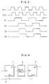
- Fig. 1 shows a portion of a shift register which is composed of a series connection of flip-flops 1 and 2.
- Fig. 2 shows a timing chart in a case on which the shift register shown in Fig. 1 is operated ideally.
- a propagation delay of a clock signal occurs, for example, in a clock wire 3 for transmitting a clock signal.
- Fig. 3 shows a timing chart at each terminal when the propagation delay of the clock signal occurs.
- the clock signals CK1 and CK2 should be inputted in the flip-flops 1 and 2 at the same time respectively.
- the clock signal CK2 is inputted in the flip-flop 2 later than the clock signal CK1. Thus, a wrong operation occurs.
- a delay circuit 4 is inserted between an output terminal Q1 of the flip-flop 1 and an input terminal D2 of the flip-flop 2 as shown in Fig. 4.
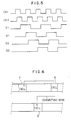
- Fig. 5 is a timing chart to show an operation of the shift register shown in Fig. 4.
- Fig. 6 shows a composition of a cell arrangement which realizes the circuit shown in Fig. 4 in accordance with the method as mentioned above.
- a delay function standard cell 5 in the same drawing corresponds to the delay circuit 4 in Fig. 4.
- standard cells 6 and 7 correspond to the flip-flop 1 and 2 respectively.
- Fig. 7 and 8 are circuit compositional diagrams of the standard cells 5 and 6 respectively.
- test circuit having a predetermined function is added in the integrated circuit.
- the methods include the serial scan method and LSSD (Level Sensitive Scan Design) method.
- a delay function is registered in a library as a cell, and then automatic place and routing is carried out by using a computer.
- the so-obtained layout presents a mode, for example, as shown in Fig. 6.
- the wiring length from the flip-flop cell 6 to the flip-flop cell 7 through the delay cell 5 depends on the position of the delay cell 5.
- the position of the delay cell 5 is not decided until the automatic place and routing of the cell is carried out. Accordingly, the degree of the signal delay and the effect of the delay cell cannot be estimated because the wiring length is not decided before the automatic place and routing.
- the delay compensation when the delay compensation is not carried out correctly, for example, a delay time owing to the delay cell is longer than the estimation, the operation speed of the integrated circuit becomes lowered. Additionally, since the delay cell is provided anew, the chip area should become larger so much.
- Fig. 9 is a partial view of a test-facilitated standard-cell-type integrated circuit based on the serial scan system.
- reference numeral 8 and 9 denote flip-flop standard cells.
- Reference numeral 10 denotes a combinational logic circuit.
- the flip-flop standard cells 8 and 9 have terminals S1 and S2 for inputting scan signals on the function test respectively.
- Output signals of the standard cell 8 are inputted into an input terminal D2 of the standard cell 9 through the logic circuit 10 (channel 8a), and directly into a scan signal input terminal S2 of the standard cell 9 (channel 8b).
- the combination of the standard cells 8 and 9 composes a shift register.
- the flip-flops are connected in the integrated circuit as shown in the drawing, the content and the state of each of the flip-flops (standard cells 8 and 9) can be read and written into an external portion at the time of the function test.
- An object of the present invention is to eliminate the above-mentioned problems. Another object of the present invention is to provide a standard-cell-type integrated circuit and a designing method thereof which can be further shortened the development term.
- a standard cell of the present invention has circuit means (comprising, e.g., a capacitor and a resistor) having a predetermined function characteristic to the standard cell, and signal delay circuit means which is provided on the input side or the output side of the standard cell to the circuit means and delays a signal inputted therein by a predetermined time.
- circuit means comprising, e.g., a capacitor and a resistor
- signal delay circuit means which is provided on the input side or the output side of the standard cell to the circuit means and delays a signal inputted therein by a predetermined time.
- the signal delay circuit means may be arranged under power source lines built in the standard cell.
- the standard cell may be so constructed that it has the same cell width as a standard cell not having the signal delay circuit means, and optionally has the same terminal positions as the one.
- the compensation for the signal propagation delay can be effected more correctly than the prior art, and the development term for the standard-cell-type integrated circuit can be shortened.
- the development term for the standard-cell-type integrated circuit can be further shortened as compared with the above-mentioned case.
- Fig. 10 shows a circuit diagram of a standard cell 11 of an embodiment of the present invention.
- the standard cell 11 (hereinafter called only "cell 11") of the embodiment has a delay circuit 12 and a flip-flop circuit 13 which is a function inherent to the cell 11.
- the delay circuit 12 comprises a resistor R, a capacitor C, and two inverters 14, 15. Input into the delay circuit 12 is carried out from an external portion through an input terminal D of the cell 11. While, output from the delay circuit 12 is supplied to the flip-flop circuit 13 which is provided in the cell 11. Accordingly, the delay circuit 12 has a function that delays a signal from the input terminal D by time corresponding to the time constant CR of the delay circuit 12, and transmits the so-delayed signal into the flip-flop circuit 13.
- Fig. 11 shows an automatic place and routing diagram in the case that a standard-cell-type integrated circuit is produced with the standard cell 11 which is the embodiment in Fig. 10.
- a standard cell 16 disposed in the lower cell row corresponds to the flip-flop 1 in Fig. 4
- the standard cell 11 disposed in the upper cell row corresponds to the flip-flop 2 and the delay circuit 4 in Fig. 4.
- the wiring mode from the cell 16 to the cell 11 depends on a relative positional relation between the standard cells 16 and 11. Therefore, estimation of a temporary wiring length before the automatic place and routing can be carried out correctly. Accordingly, a delay time in the wiring path can be correctly estimated. As the result, the delay in the wiring path can be compensated easily and correctly, and the integral circuit can effect its predetermined function.
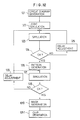
- a designing method for the standard-cell-type integrated circuit of the embodiment will be described in detail with reference to a flow chart shown in Fig. 12.
- a circuit diagram having a predetermined function is prepared (Process 121).
- a standard cell (Fig. 10) incorporating a delay circuit is designated in consideration of occurrence of a delay time in each gate.
- Process 123 is carried out again on the replaced circuit, and the result of the simulation is judged again in Process 124.
- Processes 123 and 124 are repeated till the result of the simulation can be satisfied, then a pattern for an integrated circuit is prepared (Process 126).
- the so-prepared pattern in Process 126 is equivalent to a real integrated circuit.
- Process 127 simulation based on a real wiring length of the circuit is carried out.
- Process 1211 a standard-cell-type integrated circuit chip is prepared by photolithography.
- the number of the cells can be reduced as compared with the case on which is provided anew a cell having a delay function separately. Since the undecidability of the wiring length is smaller, the number of the simulation can be reduced.
- the chip area of the integrated circuit can be reduced.
- the standard cell employed in the present invention and incorporating the delay circuit is not limited in the structure shown in Fig. 10, and for example, the delay circuit may be incorporated on the output side of th cell, or on both the input and output sides thereof.
- Fig. 13 is a circuit compositional diagram of a standard cell 17 which is another embodiment of the present invention.
- the standard cell 17 comprises a flip-flop circuit 18 and a delay circuit 19.
- the standard cell 17 has completely the same logic function as the cell 11 in Fig. 10. However, the total number of inverters used in the cells differ from each other. Namely, the cell 17 has a circuit construction in which are removed the two inverters 15 and 20 connected in series in the cell 11.
- Input of the delay circuit 19 is effected with a positive logic through an inverter 21, and output of the delay circuit 19 is effected with a negative logic. While, input of the flip-flop circuit 18 is effected with a negative logic from the delay circuit 19, and output thereof is effected with a positive logic through an inverter 22.
- the inverters can be removed as far as the delay circuit 19 and the flip-flop circuit 18 are connected in series and in the case that the delay circuit is built in one cell, when the delay circuit in the cell is not used, the standard cell has completely the same logic function.
- the area of the cell 17 becomes smaller than the area of a cell having a flip-flop function, that is, the sum of the area of the cell 6 in Fig. 8 and that of the cell 5 in Fig. 7 (area of a cell having a delay function).
- the chip area can be reduced as compared with the case of the cell 11 shown in Fig. 10.
- Fig. 14 is a compositional diagram of a delay element built in the standard cell of another embodiment according to the present invention.
- the same diagram shows a case in which a delay element, the resistor R and the capacitor C in Fig. 13 are built under power source lines 23.
- a first diffusion layer 24, a polysilicon line 25 and a second diffusion layer 26 are also built under the power source lines 23.
- a portion designated by oblique lines of the diffusion layers 24, 26 and the polysilicon line 25 composes a MOS transistor.
- first diffusion layer 24, the polysilicon line 25 and the second diffusion layer 26 respectively correspond to the electrodes of a source, a drain and a gate of the MOS transistor.
- Reference numerals 27 denotes contact holes to the power source.
- a gate capacitance of the MOS transistor corresponds to the capacitance of the condenser C in Fig. 13, while, a resistance of the polysilicon 25 corresponds to the resistance of the resistor R in Fig. 9.
- the gate capacitance can be set at a predetermined value by changing the width W of the gate portion shown in Fig. 14, so that the delay time can be also set at a predetermined value.
- the cell according to this embodiment and incorporating the delay circuit has the same width and size as a cell not incorporating the delay circuit.
- a delay function can be added in a cell without changing the width, the size, the terminal positions and the number of the terminals of the cell.
- the cell of the embodiment incorporating the delay function has the same size and terminal positions as the conventional cell, so that only the simulation in Process 127 in Fig. 12 should be repeated for the cell.
- the determination of the delay time and the delay adjustment at each location on a circuit can be carried out extremely rationally, and the development term of the standard-cell-type integrated circuit can be remarkably shortened.
- a cell incorporating the delay function and having a shape to be expanded in the vertical direction to the cell row to such an extent that each wiring area (channel) between the cell rows is not affected. In this case, the lateral length and the terminal positions of the cell are not changed.
- a relatively large transistor wiring area may be given in advance to a cell not incorporating the delay function in the pattern generation process, i.e., Process 126 in Fig. 12. Then, when it is judged that the cell should be subjected to the delay adjustment anew by the result of the simulation in Process 127 based on the real wiring length, the cell can be replaced with the cell 11 incorporating the delay function.
- the increase of the cell area is controlled as small as possible, and is more preferable that the process is carried out without the increase.
- any given free spaces in the cell may be used as the area in which the delay circuit is provided as well as using the construction shown in Fig. 14.
- the reed portion 25a of the polysilicon gate 25 may be bent in any given shape, thereby changing the resistance and the delay time thereof.
- Fig. 9 is a partial compositional diagram of the test-facilitated standard-cell-type integrated circuit. The composition in the same diagram was already described in the description of the prior art.
- Fig. 15 is an internal compositional diagram of a standard cell 30 which is employed in the test-facilitated standard-cell-type integrated circuit in Fig. 9.
- the standard cell 30 of this embodiment has a flip-flop circuit 31 and a signal delay circuit 32 as shown in Fig. 15.
- the flip-flop circuit 31 in the standard cell 30 has a usual data input terminal D, a data output terminal, a clock signal input terminal CK, a scan signal input terminal S and a terminal T for controlling switching a scan operation mode and an ordinary operation mode all over the integrated circuit.
- the delay circuit 32 is disposed between a terminal S2 for inputting a scan signal and the scan signal input terminal S of the flip-flop circuit 31 in the standard cell 30.
- a propagation delay of a clock signal is generated by the clock wiring length between the standard cells 8 and 9, and a wrong operation may be caused.
- another delay circuit 33 is disposed between a data input terminal D2 and the data input terminal D of the flip-flop circuit 31 in the standard cell 34 as shown in Fig. 16 to compensate for the clock signal delay.
- a delay circuit may be provided between a data output terminal Q1 in the cell 8 (Fig. 9) and a data output terminal (not shown in Fig. 9) of a flip-flop circuit in the cell 8 (Fig. 9).
- the gist of the present invention is applied to other methods.
- it is applicable to a bus method in which a flip-flop is connected a RAM structure.
- the standard cell and the standard-cell-type integrated circuit of the present invention it becomes possible to reduce the number of cells whose arrangement locations are not decided at the time of the pattern preparation by the automatic place and routing. Accordingly, it becomes possible to correctly set an operational timing of a circuit. Moreover, when the standard cell having the delay function and the same lateral length and terminal positions as a cell not having the delay function is employed at the position requiring the signal delay compensation, rational delay adjustment can be realized without changing the arrangement pattern which is already prepared. Accordingly, the development term for the standard-cell-type integrated circuit can be much shortened.
Landscapes
- Engineering & Computer Science (AREA)
- Computer Hardware Design (AREA)
- Physics & Mathematics (AREA)
- Theoretical Computer Science (AREA)
- Evolutionary Computation (AREA)
- Geometry (AREA)
- General Engineering & Computer Science (AREA)
- General Physics & Mathematics (AREA)
- Design And Manufacture Of Integrated Circuits (AREA)
- Semiconductor Integrated Circuits (AREA)
- Logic Circuits (AREA)
- Testing Or Measuring Of Semiconductors Or The Like (AREA)
Applications Claiming Priority (2)
| Application Number | Priority Date | Filing Date | Title |
|---|---|---|---|
| JP205688/88 | 1988-08-20 | ||
| JP63205688A JPH0255420A (ja) | 1988-08-20 | 1988-08-20 | スタンダードセルおよびスタンダードセル型集積回路 |
Publications (3)
| Publication Number | Publication Date |
|---|---|
| EP0355770A2 true EP0355770A2 (de) | 1990-02-28 |
| EP0355770A3 EP0355770A3 (de) | 1992-06-03 |
| EP0355770B1 EP0355770B1 (de) | 1997-04-02 |
Family
ID=16511061
Family Applications (1)
| Application Number | Title | Priority Date | Filing Date |
|---|---|---|---|
| EP89115382A Expired - Lifetime EP0355770B1 (de) | 1988-08-20 | 1989-08-21 | Standardzelle und integrierte Schaltung vom Standardzellen-Typ |
Country Status (4)
| Country | Link |
|---|---|
| EP (1) | EP0355770B1 (de) |
| JP (1) | JPH0255420A (de) |
| KR (1) | KR920005861B1 (de) |
| DE (1) | DE68927926T2 (de) |
Families Citing this family (2)
| Publication number | Priority date | Publication date | Assignee | Title |
|---|---|---|---|---|
| KR100408108B1 (ko) * | 2000-10-27 | 2003-12-01 | 정세영 | 류코시아니딘을 함유하는 신경아세포종 분화제 |
| JP4561036B2 (ja) * | 2003-03-03 | 2010-10-13 | ソニー株式会社 | 半導体装置及び半導体装置のレイアウト設計方法 |
Family Cites Families (1)
| Publication number | Priority date | Publication date | Assignee | Title |
|---|---|---|---|---|
| JPS6177198A (ja) * | 1984-09-21 | 1986-04-19 | Toshiba Corp | 半導体記憶装置 |
-
1988
- 1988-08-20 JP JP63205688A patent/JPH0255420A/ja active Granted
-
1989
- 1989-08-19 KR KR1019890011811A patent/KR920005861B1/ko not_active Expired
- 1989-08-21 EP EP89115382A patent/EP0355770B1/de not_active Expired - Lifetime
- 1989-08-21 DE DE68927926T patent/DE68927926T2/de not_active Expired - Fee Related
Also Published As
| Publication number | Publication date |
|---|---|
| KR920005861B1 (ko) | 1992-07-23 |
| EP0355770A3 (de) | 1992-06-03 |
| JPH05892B2 (de) | 1993-01-07 |
| KR900004003A (ko) | 1990-03-27 |
| JPH0255420A (ja) | 1990-02-23 |
| DE68927926T2 (de) | 1997-08-21 |
| EP0355770B1 (de) | 1997-04-02 |
| DE68927926D1 (de) | 1997-05-07 |
Similar Documents
| Publication | Publication Date | Title |
|---|---|---|
| US5173864A (en) | Standard cell and standard-cell-type integrated circuit | |
| EP0173945B1 (de) | Integrierte Schaltung | |
| US7263679B2 (en) | Semiconductor integrated circuit device with boundary scan test and design automation apparatus, boundary scan test method and program | |
| WO1994020909A1 (en) | Mask-programmed integrated circuits having timing and logic compatibility to user-configured logic arrays | |
| KR900002579B1 (ko) | 테스트용이화회로 및 테스트방법 | |
| US6711726B2 (en) | Automatic cell placement and routing apparatus and automatic cell placement and routing method used for the apparatus | |
| EP0809199B1 (de) | Taktverschiebungsunempfindliche Wiederordnung einer Abtastkette | |
| JP3256597B2 (ja) | 自動配置設計方法および自動配置設計装置 | |
| US6519728B2 (en) | Semiconductor integrated circuit having test circuit | |
| EP0355770A2 (de) | Standardzelle und integrierte Schaltung vom Standardzellen-Typ | |
| US6282506B1 (en) | Method of designing semiconductor integrated circuit | |
| EP0484861B1 (de) | Integriertes Schaltungsgerät mit Macro-Prüffunktion | |
| JP2550521B2 (ja) | 集積回路の配線方法 | |
| EP0422930A2 (de) | Integrierte Halbleiter-Schaltungs-Vorrichtungen | |
| JP2786017B2 (ja) | 半導体集積回路の製造方法 | |
| JPH08213467A (ja) | 半導体集積回路の設計方式 | |
| JPH10326301A (ja) | Lsi試験方式 | |
| JP3370259B2 (ja) | マスクレイアウト設計方法 | |
| JP2004207530A (ja) | 半導体集積回路及びそのレイアウト設計方法 | |
| EP1365513A2 (de) | Logische Zelle für allgemeine Verwendung, logische Matrix mit dieser Zelle und ASIC mit der Matrix | |
| JP2002076125A (ja) | 半導体集積回路のレイアウト設計方法 | |
| JPH07169839A (ja) | 半導体集積回路設計方法 | |
| JPH0863509A (ja) | シミュレーション方法 | |
| JP2002277513A (ja) | 内部遅延自動設定装置、画像処理システム用の内部遅延自動設定回路、内部遅延自動設定方法および内部遅延自動設定方法をコンピュータに実行させるプログラム | |
| JPH0685218A (ja) | 半導体集積回路 |
Legal Events
| Date | Code | Title | Description |
|---|---|---|---|
| PUAI | Public reference made under article 153(3) epc to a published international application that has entered the european phase |
Free format text: ORIGINAL CODE: 0009012 |
|
| 17P | Request for examination filed |
Effective date: 19890821 |
|
| AK | Designated contracting states |
Kind code of ref document: A2 Designated state(s): DE FR GB |
|
| PUAL | Search report despatched |
Free format text: ORIGINAL CODE: 0009013 |
|
| AK | Designated contracting states |
Kind code of ref document: A3 Designated state(s): DE FR GB |
|
| 17Q | First examination report despatched |
Effective date: 19940620 |
|
| GRAG | Despatch of communication of intention to grant |
Free format text: ORIGINAL CODE: EPIDOS AGRA |
|
| GRAH | Despatch of communication of intention to grant a patent |
Free format text: ORIGINAL CODE: EPIDOS IGRA |
|
| GRAH | Despatch of communication of intention to grant a patent |
Free format text: ORIGINAL CODE: EPIDOS IGRA |
|
| GRAA | (expected) grant |
Free format text: ORIGINAL CODE: 0009210 |
|
| AK | Designated contracting states |
Kind code of ref document: B1 Designated state(s): DE FR GB |
|
| REF | Corresponds to: |
Ref document number: 68927926 Country of ref document: DE Date of ref document: 19970507 |
|
| ET | Fr: translation filed | ||
| PGFP | Annual fee paid to national office [announced via postgrant information from national office to epo] |
Ref country code: FR Payment date: 19970811 Year of fee payment: 9 |
|
| PGFP | Annual fee paid to national office [announced via postgrant information from national office to epo] |
Ref country code: GB Payment date: 19970812 Year of fee payment: 9 |
|
| PLBE | No opposition filed within time limit |
Free format text: ORIGINAL CODE: 0009261 |
|
| STAA | Information on the status of an ep patent application or granted ep patent |
Free format text: STATUS: NO OPPOSITION FILED WITHIN TIME LIMIT |
|
| 26N | No opposition filed | ||
| PG25 | Lapsed in a contracting state [announced via postgrant information from national office to epo] |
Ref country code: GB Free format text: LAPSE BECAUSE OF NON-PAYMENT OF DUE FEES Effective date: 19980821 |
|
| GBPC | Gb: european patent ceased through non-payment of renewal fee |
Effective date: 19980821 |
|
| PG25 | Lapsed in a contracting state [announced via postgrant information from national office to epo] |
Ref country code: FR Free format text: LAPSE BECAUSE OF NON-PAYMENT OF DUE FEES Effective date: 19990430 |
|
| REG | Reference to a national code |
Ref country code: FR Ref legal event code: ST |
|
| PGFP | Annual fee paid to national office [announced via postgrant information from national office to epo] |
Ref country code: DE Payment date: 20070816 Year of fee payment: 19 |
|
| PG25 | Lapsed in a contracting state [announced via postgrant information from national office to epo] |
Ref country code: DE Free format text: LAPSE BECAUSE OF NON-PAYMENT OF DUE FEES Effective date: 20090303 |