EP0355865A2 - Milieu d'enregistrement avec information optique réversible - Google Patents
Milieu d'enregistrement avec information optique réversible Download PDFInfo
- Publication number
- EP0355865A2 EP0355865A2 EP89118260A EP89118260A EP0355865A2 EP 0355865 A2 EP0355865 A2 EP 0355865A2 EP 89118260 A EP89118260 A EP 89118260A EP 89118260 A EP89118260 A EP 89118260A EP 0355865 A2 EP0355865 A2 EP 0355865A2
- Authority
- EP
- European Patent Office
- Prior art keywords
- composition
- information recording
- recording film
- recording medium
- anyone
- Prior art date
- Legal status (The legal status is an assumption and is not a legal conclusion. Google has not performed a legal analysis and makes no representation as to the accuracy of the status listed.)
- Granted
Links
Images



Classifications
-
- G—PHYSICS
- G11—INFORMATION STORAGE
- G11B—INFORMATION STORAGE BASED ON RELATIVE MOVEMENT BETWEEN RECORD CARRIER AND TRANSDUCER
- G11B7/00—Recording or reproducing by optical means, e.g. recording using a thermal beam of optical radiation by modifying optical properties or the physical structure, reproducing using an optical beam at lower power by sensing optical properties; Record carriers therefor
- G11B7/24—Record carriers characterised by shape, structure or physical properties, or by the selection of the material
- G11B7/241—Record carriers characterised by shape, structure or physical properties, or by the selection of the material characterised by the selection of the material
- G11B7/242—Record carriers characterised by shape, structure or physical properties, or by the selection of the material characterised by the selection of the material of recording layers
- G11B7/243—Record carriers characterised by shape, structure or physical properties, or by the selection of the material characterised by the selection of the material of recording layers comprising inorganic materials only, e.g. ablative layers
- G11B7/2433—Metals or elements of Groups 13, 14, 15 or 16 of the Periodic Table, e.g. B, Si, Ge, As, Sb, Bi, Se or Te
-
- G—PHYSICS
- G11—INFORMATION STORAGE
- G11B—INFORMATION STORAGE BASED ON RELATIVE MOVEMENT BETWEEN RECORD CARRIER AND TRANSDUCER
- G11B7/00—Recording or reproducing by optical means, e.g. recording using a thermal beam of optical radiation by modifying optical properties or the physical structure, reproducing using an optical beam at lower power by sensing optical properties; Record carriers therefor
- G11B7/24—Record carriers characterised by shape, structure or physical properties, or by the selection of the material
- G11B7/241—Record carriers characterised by shape, structure or physical properties, or by the selection of the material characterised by the selection of the material
- G11B7/242—Record carriers characterised by shape, structure or physical properties, or by the selection of the material characterised by the selection of the material of recording layers
- G11B7/243—Record carriers characterised by shape, structure or physical properties, or by the selection of the material characterised by the selection of the material of recording layers comprising inorganic materials only, e.g. ablative layers
-
- G—PHYSICS
- G11—INFORMATION STORAGE
- G11B—INFORMATION STORAGE BASED ON RELATIVE MOVEMENT BETWEEN RECORD CARRIER AND TRANSDUCER
- G11B7/00—Recording or reproducing by optical means, e.g. recording using a thermal beam of optical radiation by modifying optical properties or the physical structure, reproducing using an optical beam at lower power by sensing optical properties; Record carriers therefor
- G11B7/24—Record carriers characterised by shape, structure or physical properties, or by the selection of the material
- G11B7/241—Record carriers characterised by shape, structure or physical properties, or by the selection of the material characterised by the selection of the material
- G11B7/242—Record carriers characterised by shape, structure or physical properties, or by the selection of the material characterised by the selection of the material of recording layers
- G11B7/243—Record carriers characterised by shape, structure or physical properties, or by the selection of the material characterised by the selection of the material of recording layers comprising inorganic materials only, e.g. ablative layers
- G11B2007/24302—Metals or metalloids
- G11B2007/24312—Metals or metalloids group 14 elements (e.g. Si, Ge, Sn)
-
- G—PHYSICS
- G11—INFORMATION STORAGE
- G11B—INFORMATION STORAGE BASED ON RELATIVE MOVEMENT BETWEEN RECORD CARRIER AND TRANSDUCER
- G11B7/00—Recording or reproducing by optical means, e.g. recording using a thermal beam of optical radiation by modifying optical properties or the physical structure, reproducing using an optical beam at lower power by sensing optical properties; Record carriers therefor
- G11B7/24—Record carriers characterised by shape, structure or physical properties, or by the selection of the material
- G11B7/241—Record carriers characterised by shape, structure or physical properties, or by the selection of the material characterised by the selection of the material
- G11B7/242—Record carriers characterised by shape, structure or physical properties, or by the selection of the material characterised by the selection of the material of recording layers
- G11B7/243—Record carriers characterised by shape, structure or physical properties, or by the selection of the material characterised by the selection of the material of recording layers comprising inorganic materials only, e.g. ablative layers
- G11B2007/24302—Metals or metalloids
- G11B2007/24314—Metals or metalloids group 15 elements (e.g. Sb, Bi)
-
- G—PHYSICS
- G11—INFORMATION STORAGE
- G11B—INFORMATION STORAGE BASED ON RELATIVE MOVEMENT BETWEEN RECORD CARRIER AND TRANSDUCER
- G11B7/00—Recording or reproducing by optical means, e.g. recording using a thermal beam of optical radiation by modifying optical properties or the physical structure, reproducing using an optical beam at lower power by sensing optical properties; Record carriers therefor
- G11B7/24—Record carriers characterised by shape, structure or physical properties, or by the selection of the material
- G11B7/241—Record carriers characterised by shape, structure or physical properties, or by the selection of the material characterised by the selection of the material
- G11B7/242—Record carriers characterised by shape, structure or physical properties, or by the selection of the material characterised by the selection of the material of recording layers
- G11B7/243—Record carriers characterised by shape, structure or physical properties, or by the selection of the material characterised by the selection of the material of recording layers comprising inorganic materials only, e.g. ablative layers
- G11B2007/24302—Metals or metalloids
- G11B2007/24316—Metals or metalloids group 16 elements (i.e. chalcogenides, Se, Te)
-
- G—PHYSICS
- G11—INFORMATION STORAGE
- G11B—INFORMATION STORAGE BASED ON RELATIVE MOVEMENT BETWEEN RECORD CARRIER AND TRANSDUCER
- G11B7/00—Recording or reproducing by optical means, e.g. recording using a thermal beam of optical radiation by modifying optical properties or the physical structure, reproducing using an optical beam at lower power by sensing optical properties; Record carriers therefor
- G11B7/004—Recording, reproducing or erasing methods; Read, write or erase circuits therefor
- G11B7/0045—Recording
- G11B7/00454—Recording involving phase-change effects
-
- G—PHYSICS
- G11—INFORMATION STORAGE
- G11B—INFORMATION STORAGE BASED ON RELATIVE MOVEMENT BETWEEN RECORD CARRIER AND TRANSDUCER
- G11B7/00—Recording or reproducing by optical means, e.g. recording using a thermal beam of optical radiation by modifying optical properties or the physical structure, reproducing using an optical beam at lower power by sensing optical properties; Record carriers therefor
- G11B7/24—Record carriers characterised by shape, structure or physical properties, or by the selection of the material
- G11B7/241—Record carriers characterised by shape, structure or physical properties, or by the selection of the material characterised by the selection of the material
- G11B7/252—Record carriers characterised by shape, structure or physical properties, or by the selection of the material characterised by the selection of the material of layers other than recording layers
- G11B7/253—Record carriers characterised by shape, structure or physical properties, or by the selection of the material characterised by the selection of the material of layers other than recording layers of substrates
- G11B7/2531—Record carriers characterised by shape, structure or physical properties, or by the selection of the material characterised by the selection of the material of layers other than recording layers of substrates comprising glass
-
- G—PHYSICS
- G11—INFORMATION STORAGE
- G11B—INFORMATION STORAGE BASED ON RELATIVE MOVEMENT BETWEEN RECORD CARRIER AND TRANSDUCER
- G11B7/00—Recording or reproducing by optical means, e.g. recording using a thermal beam of optical radiation by modifying optical properties or the physical structure, reproducing using an optical beam at lower power by sensing optical properties; Record carriers therefor
- G11B7/24—Record carriers characterised by shape, structure or physical properties, or by the selection of the material
- G11B7/241—Record carriers characterised by shape, structure or physical properties, or by the selection of the material characterised by the selection of the material
- G11B7/252—Record carriers characterised by shape, structure or physical properties, or by the selection of the material characterised by the selection of the material of layers other than recording layers
- G11B7/253—Record carriers characterised by shape, structure or physical properties, or by the selection of the material characterised by the selection of the material of layers other than recording layers of substrates
- G11B7/2533—Record carriers characterised by shape, structure or physical properties, or by the selection of the material characterised by the selection of the material of layers other than recording layers of substrates comprising resins
-
- G—PHYSICS
- G11—INFORMATION STORAGE
- G11B—INFORMATION STORAGE BASED ON RELATIVE MOVEMENT BETWEEN RECORD CARRIER AND TRANSDUCER
- G11B7/00—Recording or reproducing by optical means, e.g. recording using a thermal beam of optical radiation by modifying optical properties or the physical structure, reproducing using an optical beam at lower power by sensing optical properties; Record carriers therefor
- G11B7/24—Record carriers characterised by shape, structure or physical properties, or by the selection of the material
- G11B7/241—Record carriers characterised by shape, structure or physical properties, or by the selection of the material characterised by the selection of the material
- G11B7/252—Record carriers characterised by shape, structure or physical properties, or by the selection of the material characterised by the selection of the material of layers other than recording layers
- G11B7/257—Record carriers characterised by shape, structure or physical properties, or by the selection of the material characterised by the selection of the material of layers other than recording layers of layers having properties involved in recording or reproduction, e.g. optical interference layers or sensitising layers or dielectric layers, which are protecting the recording layers
-
- G—PHYSICS
- G11—INFORMATION STORAGE
- G11B—INFORMATION STORAGE BASED ON RELATIVE MOVEMENT BETWEEN RECORD CARRIER AND TRANSDUCER
- G11B7/00—Recording or reproducing by optical means, e.g. recording using a thermal beam of optical radiation by modifying optical properties or the physical structure, reproducing using an optical beam at lower power by sensing optical properties; Record carriers therefor
- G11B7/24—Record carriers characterised by shape, structure or physical properties, or by the selection of the material
- G11B7/26—Apparatus or processes specially adapted for the manufacture of record carriers
- G11B7/266—Sputtering or spin-coating layers
-
- Y—GENERAL TAGGING OF NEW TECHNOLOGICAL DEVELOPMENTS; GENERAL TAGGING OF CROSS-SECTIONAL TECHNOLOGIES SPANNING OVER SEVERAL SECTIONS OF THE IPC; TECHNICAL SUBJECTS COVERED BY FORMER USPC CROSS-REFERENCE ART COLLECTIONS [XRACs] AND DIGESTS
- Y10—TECHNICAL SUBJECTS COVERED BY FORMER USPC
- Y10S—TECHNICAL SUBJECTS COVERED BY FORMER USPC CROSS-REFERENCE ART COLLECTIONS [XRACs] AND DIGESTS
- Y10S430/00—Radiation imagery chemistry: process, composition, or product thereof
- Y10S430/146—Laser beam
Definitions
- the present invention relates to phase-change type, reversible optical information-recording medium, being suitable for recording, reproducing, erasing, and rewriting of information, by use of a laser beam.
- Te-based alloy film produces comparatively easily reversible phase transition by irradiation of a laser beam. Since, among them, the composition rich in Te-component makes it possible to obtain an amorphous state by relatively low power of laser, the application to recording medium has been so far tried.
- the object of this invention is to supply a reversible optical information-recording medium with the improved erasing speed without reduction of recording sensitivity. Also, the other object of this invention is to supply a reversible optical information-recording medium with long cyclability of recording/erasing. Moreover, the other object is to supply a reversible optical information-recording medium unchangeable in thermal stability and with igh reliability even after repeating runs of recording and erasing.
- an optical information-recording medium of this invention consists of a recording layer (4) sandwiched by dielectric thin films (2, 3) such as SiO2, Al2O3, ZnS on substrate (1) with flat surface, made of plastics such as PMMA and polycarbonate, metals such as Al and Cu or glass, etc.
- the dielectric layer is not always necessary, but it is effective in reducing thermal damage of plastic materials or the transformation and evaporation of the recording layer itself caused by repeating irradiation of laser beam. It is also possible to stick a protecting plate on this layer.
- a recording layer consists of ternary compositionscontaining Te, Ge, Bi, or quarternary compositionscontaining the fourth element of Se with which a part of Te is replaced.
- the main composition is located on the line linking the composition points of Ge50Te50 and 20 ⁇ (Bi2Te3).
- the main composition is shown by the following formula: x ⁇ 50 Ge(Te,Se) + (1-x) ⁇ 20 Bi2(Te,Se)3;or (Te,Se) 60-10x Ge 50x (Bi) 40-40x (wherein 0.05 ⁇ x ⁇ 0.8)
- concentration of Se is not related to the value of x, and it is 30 atomic % or less of whole, namely its maximum value is 30 atomic %.
- Each composition is permitted to have some range as shown in Fig. 2(b) as a domain.
- Te alloy with only one kind of additive element such as CdTe, SnTe, PbTe, InTe, Sb2Te3, and GeTe, is unsuitable for a recording layer by one or all of the following reasons:
- the trial is to lower the melting point by composing solid solution of plural Te-alloys and, at the same time, to make amorphous phase stable. It is not enough to make solid solution with low melting point, but it is necessary to obtain the solid solution to be difficult in bringing about phase-separation by repeating run of recording/erasing and to have sufficiently high (not too high) crystallization rate.
- the above-mentioned compounds have mutually similar crystal structures, and have very close characteristics. This fact affords the following effect: even if the composition of film would not strictly coincide with one phase of the above-mentioned stoichiometric compounds, characteristics are unfirom throughout broad range of composition as a whole, as the whole could be regarded as the mixture of the above-mentioned three phases. Therefore, there is a merit that there is almost no change in the film characteristics, even if the phase separation has occurred by the repeating runs of recording/erasing, except the case of which the complete separation up to the composition at both ends occurs.
- the melting points of the above-mentioned phases are low and close to each other.
- the melting point in the system of GeTe - Bi2Te3 is near 570°C; as it is lower by more than 100°C comparing with 725°C of GeTe single substance, melting by a laser beam could be performed relatively easily.
- the fourth point has been found in the crystallization process.
- the stable crystal form is hexagonal, but in the crystallization process by laser radiation, single phase of NaCl-type cubic system consisting of ternary elements, Ge, Te and Bi, is obtained first (this is also the case with Se). It is advantageous that the crystal form obtained is as isotropic as possible (namely, near the atomic structure of liquid phase or amorphous phase) in order to promote smoothly the crystallization. It is assumed that the diffusion distance of atom is shortened and then the annealing time necessary for crystallization is shortened.
- Se is added only in the form of replacement of Te, so that the balance of the concentration between Te and Ge, Bi is not demolished.
- the first addition effect of Se is to increase the viscosity of the system. Added Se forms the Se-compounds, such as GeSe, GeSe2, Bi2Se3, when film is crystallized. As these compounds have higher bond energy than the corresponding Te-compounds of the same elements, they are not completely separated even at liquid phase. Therefore, the molten liquid has the high viscosity, and it becomes easy to form amorphous phase. In other words, the condition of rapid cooling to form an amorphous phase becomes slightly mild. It is important that this characteristic does not show the incontinuous change by the addition of Se.
- the second addition effect of Se is to raise the crystallization temperature of the system. It is especially effective in poor composition of GeTe-component, and it acts to raise the stability of amorphous phase (the recorded signal).
- the melting point does not so change by addition of Se. It is assumed that this is due to the near melting point between Te- and Se-compounds of the same elements. It is very important that the recording sensitivity does not decrease by the addition of Se.
- a recording medium of this invention could be produced by the method, such as vacuum deposition and sputtering.
- sputtering it is possible to use an alloy target designed from the desirable composition or a complex mosaic target with the area corresponding to each composition ratio.
- the co-evaporation method with plural sources is convenient to control the composition.
- it is important that the deposition rate from each source is perfectly independently controlled by preparing for four electron guns and their electric sources and four sensors of film thickness (for example, quartz oscillator).
- the degree of vacuum at deposition is enough at 1.3 ⁇ 10 ⁇ 2 to 10 ⁇ 5 Pa (10 ⁇ 4 - 10 ⁇ 7 torr).
- Sample pieces of the recording film containing triple elements of Te, Ge and Bi with various compositions were prepared by the above-described vacuum deposition method, and these characteristics were investigated.
- the substrate of sample piece is a glass disk with thickness of 0.3 mm and diameter ( ⁇ ) of 8 mm; the film thickness of a recording layer is about 1000 ⁇ .
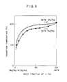
- Fig. 3 shows the behavior of Tx in the compositions on the line which links the composition point of GeTe and that of Bi2Te3 at the triangle diagram of Ge-Te-Bi.
- phase transition temperature in the system GeTe - Bi2Te3 is higher than 100°C (sufficiently higher than room temperature) in the case of more than 3 - 5% of x in the above-mentioned formula, and it shows that the amorphous phase is very stable.
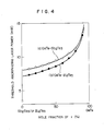
- Fig. 4 shows the sensitivity of amorphization, Pa in the same composition as above. From this figure, Pa in the system of GeTe - Bi2Te3 has a tendency to increase as the proportion of GeTe increases, and it increases very much in the case of more than 80 - 90% of x proportion. Namely, if the proportion of GeTe is in the region of 80% or less of x, it is shown that a high recording sensitivity could be obtained.
- Fig. 5 shows ⁇ x1 and ⁇ x2, the irradiation time necessary for beginning of crystallization in the same composition as above. From this figure, it is found that ⁇ x1 has a tendency to increase as the proportion of GeTe increases, ⁇ x2 has a tendency to increase as the proportion of GeTe decreases, and it does not exist in the case of less than 30% of x.
- the curves of ⁇ x1 and ⁇ x2 cross at around 30 - 40 mol% of x-concentration. Therefore, it is found that the region of 5 - 40% of x in the composition ratio is suitable for erasing method of solid phase and the region of 40% or more of x ratio is suitable for erasing method of liquid phase.
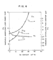
- Fig. 6 shows the change in the sensitivity of amorphization Pa, and the crystallization time ⁇ x1 and ⁇ x2 with the change in Se concentration. From this figure, it is found that Pa decreases by addition of Se, and saturates at about 10 atomic %, ⁇ x1 and ⁇ x2 increases continuously and monotonically as the concentration of Se increases. ⁇ x1 increases extremely over 20 atomic % of Se concentration; ⁇ x2 increases monotonically until the concentration of Se is about 15 atomic %, but it does not exist at higher than 15 atomic % of Se concentration (namely, crystallization becomes difficult)
- Example 2 The same experiment as adopted in Example 1 was undertaken to the composition come off the above-mentioned composition-line. Fixing the concentration of Ge for the composition on the above line, the composition ratio of Bi was changed in the range of ⁇ 15 atomic %. As a result, the large difference from the composition on the line was not produced as to Tx and Pa, but ⁇ x showed a rather large value when the composition came off the line to both sides.
- the disk was prepared, and the repeating characteristics of recording/erasing were investigated.
- An optical disk was prepared by laminating ZnS and a recording layer in the order, i.e. ZnS, a recording layer, ZnS ..., on the substrate of PMMA resin of 130 mm in diameter and thickness of 1.2 mm with the light guide-track, and the protecting plate using the UV-ray curing resin on the surface.
- the thickness of each layer was about 80 nm, 100 nm and 160 nm (800 ⁇ , 1000 ⁇ , and 1600 ⁇ ) in the order from the lowest layer to the upper ones, and these were designed to raise the effect of light-absorption in the recording layer.
- a laser beam was supplied from the side of substrate.
- a dynamic tester (deck) was equipped with a circular laser spot of 0.9 ⁇ m in diameter for recording and an elliptic laser spot of 1 x 8 ⁇ m for erasing, and the two spots were continuously arranged in one optical head.
- the repeating life of recording/erasing was investigated at a peripheral speed of 5 m/s.
- Each power of recording and erasing was suitably selected according to the disk characteristics, and the recording was made at simple frequency mode of 2 MHz.
- the limit of life was defined as the number of times showing the decrease of 3 dB from initial C/N.
- the following conclusions of 1) - 4) were obtained.
- the results of the initial C/N of 53 dB and the C/N of 51 dB after 105 time repeating were obtained by repeating recording/erasing at recording power of 8 mW and erasing power of 8 mW.
- the results of the initial C/N of 54 dB and the C/N of 52 dB after 105 times repeating were obtained by repeating recording/erasing at recording power of 7 mW and erasing power of 10 mW.
Landscapes
- Chemical & Material Sciences (AREA)
- Inorganic Chemistry (AREA)
- Optical Record Carriers And Manufacture Thereof (AREA)
- Thermal Transfer Or Thermal Recording In General (AREA)
Applications Claiming Priority (9)
| Application Number | Priority Date | Filing Date | Title |
|---|---|---|---|
| JP211471/85 | 1985-09-25 | ||
| JP60211470A JPS6273438A (ja) | 1985-09-25 | 1985-09-25 | 光学情報記録部材 |
| JP211470/85 | 1985-09-25 | ||
| JP60211471A JPS6273439A (ja) | 1985-09-25 | 1985-09-25 | 光学情報記録部材 |
| JP53034/86 | 1986-03-11 | ||
| JP53033/86 | 1986-03-11 | ||
| JP61053033A JP2592800B2 (ja) | 1986-03-11 | 1986-03-11 | 光学情報記録部材 |
| JP61053034A JP2584741B2 (ja) | 1986-03-11 | 1986-03-11 | 書換え可能な光学情報記録部材 |
| EP86113211A EP0217293B1 (fr) | 1985-09-25 | 1986-09-25 | Utilisation de compositions en tant que medium optique réversible pour l'enregistrement d'informations |
Related Parent Applications (1)
| Application Number | Title | Priority Date | Filing Date |
|---|---|---|---|
| EP86113211.6 Division | 1986-09-25 |
Publications (3)
| Publication Number | Publication Date |
|---|---|
| EP0355865A2 true EP0355865A2 (fr) | 1990-02-28 |
| EP0355865A3 EP0355865A3 (en) | 1990-03-28 |
| EP0355865B1 EP0355865B1 (fr) | 1994-06-01 |
Family
ID=27462854
Family Applications (2)
| Application Number | Title | Priority Date | Filing Date |
|---|---|---|---|
| EP89118260A Expired - Lifetime EP0355865B1 (fr) | 1985-09-25 | 1986-09-25 | Milieu d'enregistrement avec information optique réversible |
| EP86113211A Expired - Lifetime EP0217293B1 (fr) | 1985-09-25 | 1986-09-25 | Utilisation de compositions en tant que medium optique réversible pour l'enregistrement d'informations |
Family Applications After (1)
| Application Number | Title | Priority Date | Filing Date |
|---|---|---|---|
| EP86113211A Expired - Lifetime EP0217293B1 (fr) | 1985-09-25 | 1986-09-25 | Utilisation de compositions en tant que medium optique réversible pour l'enregistrement d'informations |
Country Status (5)
| Country | Link |
|---|---|
| US (4) | US5278011A (fr) |
| EP (2) | EP0355865B1 (fr) |
| KR (1) | KR900009187B1 (fr) |
| CN (1) | CN1010519B (fr) |
| DE (2) | DE3689886T2 (fr) |
Cited By (4)
| Publication number | Priority date | Publication date | Assignee | Title |
|---|---|---|---|---|
| WO1996000441A1 (fr) * | 1994-06-23 | 1996-01-04 | Philips Electronics N.V. | Support optique d'informations |
| EP0751505A3 (fr) * | 1995-06-27 | 1998-07-08 | Kabushiki Kaisha Toshiba | Milieu d'enregistrement optique d'information |
| US7709073B2 (en) | 2004-07-28 | 2010-05-04 | Panasonic Corporation | Information recording medium |
| US7829169B2 (en) | 2005-06-07 | 2010-11-09 | Panasonic Corporation | Information recording medium and method for producing the same |
Families Citing this family (36)
| Publication number | Priority date | Publication date | Assignee | Title |
|---|---|---|---|---|
| CN1010519B (zh) * | 1985-09-25 | 1990-11-21 | 松下电器产业株式会社 | 可逆的光学情报记录介质 |
| JPS63251290A (ja) * | 1987-04-08 | 1988-10-18 | Hitachi Ltd | 光記録媒体と記録・再生方法及びその応用 |
| DE3885156T2 (de) * | 1987-06-11 | 1994-03-17 | Asahi Chemical Ind | Verfahren zum Aufzeichnen und Löschen von Daten. |
| JPH081707B2 (ja) * | 1987-12-04 | 1996-01-10 | 松下電器産業株式会社 | 光学的情報記録媒体 |
| US5273861A (en) * | 1987-12-04 | 1993-12-28 | Matsushita Electric Industrial Co., Ltd. | Optical information recording medium, method of making an optical information recording medium and method of recording/reproducing optical information |
| US5063097A (en) * | 1988-12-16 | 1991-11-05 | Toray Industries, Inc. | Optical recording medium |
| EP0392179B1 (fr) * | 1989-02-28 | 1995-11-08 | Fuji Xerox Co., Ltd. | Support d'enregistrement optique |
| US5268254A (en) * | 1989-02-28 | 1993-12-07 | Fuji Xerox Co., Ltd. | Optical recording medium |
| US5128099A (en) * | 1991-02-15 | 1992-07-07 | Energy Conversion Devices, Inc. | Congruent state changeable optical memory material and device |
| CN1303588C (zh) * | 1991-06-04 | 2007-03-07 | 三菱电机株式会社 | 光学数据存贮介质 |
| US6821707B2 (en) * | 1996-03-11 | 2004-11-23 | Matsushita Electric Industrial Co., Ltd. | Optical information recording medium, producing method thereof and method of recording/erasing/reproducing information |
| EP0951717B1 (fr) * | 1997-11-07 | 2005-06-22 | Koninklijke Philips Electronics N.V. | SUPPORT D'INFORMATION OPTIQUE REENREGISTRABLE COMPRENANT UN ALLIAGE Ge-Sb-Te |
| TW421790B (en) * | 1998-04-20 | 2001-02-11 | Koninkl Philips Electronics Nv | Rewritable optical information medium |
| DE60034974T2 (de) * | 1999-03-15 | 2008-01-24 | Matsushita Electric Industrial Co., Ltd., Kadoma | Optisches Phasenübergangsaufzeichnungsmedium und Herstellungsverfahren |
| TW484126B (en) | 1999-03-26 | 2002-04-21 | Matsushita Electric Industrial Co Ltd | Manufacturing and recording regeneration method for information record medium |
| EP1372146B1 (fr) | 1999-05-19 | 2007-11-14 | Mitsubishi Kagaku Media Co., Ltd. | Méthode d'enregistrement optique et milieu d'enregistrement |
| TW487682B (en) | 2000-08-10 | 2002-05-21 | Nat Science Council | Rewritable phase-change type optical information recording composition and optical disk containing the same |
| DE60012954T2 (de) * | 2000-12-19 | 2005-01-05 | National Science Council | Optisches Aufzeichnungsmaterial mit Phasenänderung, das wiederbeschreibbar ist, und wiederbeschreibbare, optische Platte mit Phasenänderung |
| EP2112659A1 (fr) * | 2001-09-01 | 2009-10-28 | Energy Convertion Devices, Inc. | Stockage de données augmenté dans une mémoire optique et systèmes de récuperation faisant appel à des lasers bleus et/ou des lentilles a plasmons |
| US7115927B2 (en) * | 2003-02-24 | 2006-10-03 | Samsung Electronics Co., Ltd. | Phase changeable memory devices |
| US7402851B2 (en) * | 2003-02-24 | 2008-07-22 | Samsung Electronics Co., Ltd. | Phase changeable memory devices including nitrogen and/or silicon and methods for fabricating the same |
| US7425735B2 (en) * | 2003-02-24 | 2008-09-16 | Samsung Electronics Co., Ltd. | Multi-layer phase-changeable memory devices |
| JP4181490B2 (ja) * | 2003-03-25 | 2008-11-12 | 松下電器産業株式会社 | 情報記録媒体とその製造方法 |
| TW200529414A (en) * | 2004-02-06 | 2005-09-01 | Renesas Tech Corp | Storage |
| TW200601322A (en) * | 2004-04-07 | 2006-01-01 | Hitachi Maxell | Information recording medium |
| TWI312998B (en) * | 2005-12-23 | 2009-08-01 | Ind Tech Res Inst | Phase-change recording layer and method of manufacturing the same and phase-change recording cell using such recording layer |
| KR100782482B1 (ko) * | 2006-05-19 | 2007-12-05 | 삼성전자주식회사 | GeBiTe막을 상변화 물질막으로 채택하는 상변화 기억 셀, 이를 구비하는 상변화 기억소자, 이를 구비하는 전자 장치 및 그 제조방법 |
| EP2055495A4 (fr) * | 2006-08-08 | 2010-11-03 | Panasonic Corp | Support d'enregistrement d'informations, son procédé de fabrication, et cible de pulvérisation cathodique |
| KR100810615B1 (ko) * | 2006-09-20 | 2008-03-06 | 삼성전자주식회사 | 고온 상전이 패턴을 구비한 상전이 메모리소자 및 그제조방법 |
| US8273438B2 (en) * | 2007-02-09 | 2012-09-25 | Panasonic Corporation | Information recording medium, process for producing the information recording medium, sputtering target and film forming apparatus |
| JP2009178974A (ja) * | 2008-01-31 | 2009-08-13 | Toshiba Corp | 情報記録媒体 |
| US8040765B2 (en) * | 2008-09-05 | 2011-10-18 | Panasonic Corporation | Initialization method for information recording medium, initialization apparatus for information recording medium, and information recording medium |
| JPWO2010041373A1 (ja) * | 2008-10-06 | 2012-03-01 | パナソニック株式会社 | 情報記録媒体とその製造方法、及びスパッタリングターゲット |
| WO2011024381A1 (fr) * | 2009-08-31 | 2011-03-03 | パナソニック株式会社 | Support d'enregistrement d'informations et procédé de fabrication de ce support |
| WO2013031107A1 (fr) | 2011-08-30 | 2013-03-07 | パナソニック株式会社 | Support d'enregistrement d'informations optiques et procédé pour sa fabrication |
| DE102018203241A1 (de) | 2018-03-05 | 2019-09-05 | Carl Zeiss Smt Gmbh | Optisches Element, sowie Verfahren zur Korrektur der Wellenfrontwirkung eines optischen Elements |
Family Cites Families (24)
| Publication number | Priority date | Publication date | Assignee | Title |
|---|---|---|---|---|
| US3530441A (en) * | 1969-01-15 | 1970-09-22 | Energy Conversion Devices Inc | Method and apparatus for storing and retrieving information |
| US3868651A (en) * | 1970-08-13 | 1975-02-25 | Energy Conversion Devices Inc | Method and apparatus for storing and reading data in a memory having catalytic material to initiate amorphous to crystalline change in memory structure |
| NL8301956A (nl) * | 1983-06-02 | 1985-01-02 | Optical Storage Int | Optisch registratie element. |
| JPS6034897A (ja) * | 1983-08-08 | 1985-02-22 | Nippon Telegr & Teleph Corp <Ntt> | 書替可能光記録媒体 |
| JPS6042095A (ja) * | 1983-08-19 | 1985-03-06 | Hitachi Ltd | 情報の記録用部材およびその製造方法 |
| JPS6048397A (ja) * | 1983-08-29 | 1985-03-16 | Nippon Telegr & Teleph Corp <Ntt> | 光学的記録媒体およびその製造方法 |
| JPS6058893A (ja) * | 1983-09-12 | 1985-04-05 | Nippon Telegr & Teleph Corp <Ntt> | 光記録媒体 |
| JPS60135951A (ja) * | 1983-12-24 | 1985-07-19 | Fujitsu Ltd | パタ−ン形成法 |
| JPS60155495A (ja) * | 1984-01-26 | 1985-08-15 | Sony Corp | 光学情報記録媒体 |
| JPS60155496A (ja) * | 1984-01-26 | 1985-08-15 | Sony Corp | 情報記録媒体 |
| JPS60157894A (ja) * | 1984-01-27 | 1985-08-19 | Nippon Columbia Co Ltd | 光情報記録媒体 |
| JPS60219646A (ja) * | 1984-04-16 | 1985-11-02 | Nippon Columbia Co Ltd | 光情報記録媒体 |
| JPS60234248A (ja) * | 1984-05-07 | 1985-11-20 | Nippon Columbia Co Ltd | 光情報記録媒体 |
| US4656079A (en) * | 1984-06-15 | 1987-04-07 | Matsushita Electric Industrial Co., Ltd. | Reversible optical information recording medium |
| JPS6131291A (ja) * | 1984-07-24 | 1986-02-13 | Daicel Chem Ind Ltd | 光学的情報記録媒体 |
| JPS6189889A (ja) * | 1984-10-11 | 1986-05-08 | Nippon Columbia Co Ltd | 光情報記録媒体 |
| CN1008845B (zh) * | 1984-12-05 | 1990-07-18 | 富士通株式会社 | 光学信息记录介质及信息的记录与擦抹的方法 |
| US4670345A (en) * | 1985-02-22 | 1987-06-02 | Asahi Kasei Kogyo Kabushiki Kaisha | Information recording medium |
| US4787077A (en) * | 1985-08-15 | 1988-11-22 | International Business Machines Corporation | Process for optically storing information using materials having a single phase in both the crystalline state and the amorphous state |
| CN1010519B (zh) * | 1985-09-25 | 1990-11-21 | 松下电器产业株式会社 | 可逆的光学情报记录介质 |
| JPS6431291A (en) * | 1987-07-27 | 1989-02-01 | Oki Electric Ind Co Ltd | Automatic goods renting apparatus |
| JPS6489889A (en) * | 1987-09-30 | 1989-04-05 | Toshiba Corp | User's termination system |
| JP2696858B2 (ja) * | 1987-10-28 | 1998-01-14 | 松下電器産業株式会社 | 光学情報記録再生消去部材 |
| US5238572A (en) * | 1993-01-25 | 1993-08-24 | Betz Laboratories, Inc. | Enzyme treatment for industrial slime control |
-
1986
- 1986-09-22 CN CN86107003A patent/CN1010519B/zh not_active Expired
- 1986-09-23 KR KR1019860007937A patent/KR900009187B1/ko not_active Expired
- 1986-09-25 EP EP89118260A patent/EP0355865B1/fr not_active Expired - Lifetime
- 1986-09-25 EP EP86113211A patent/EP0217293B1/fr not_active Expired - Lifetime
- 1986-09-25 DE DE3689886T patent/DE3689886T2/de not_active Expired - Fee Related
- 1986-09-25 DE DE3689815T patent/DE3689815T2/de not_active Expired - Lifetime
-
1993
- 1993-04-28 US US08/053,346 patent/US5278011A/en not_active Expired - Lifetime
- 1993-04-28 US US08/053,343 patent/US6268107B1/en not_active Ceased
-
2001
- 2001-01-22 US US09/765,677 patent/US20010019810A1/en not_active Abandoned
-
2003
- 2003-03-14 US US10/389,615 patent/USRE42222E1/en not_active Expired - Lifetime
Cited By (5)
| Publication number | Priority date | Publication date | Assignee | Title |
|---|---|---|---|---|
| WO1996000441A1 (fr) * | 1994-06-23 | 1996-01-04 | Philips Electronics N.V. | Support optique d'informations |
| EP0751505A3 (fr) * | 1995-06-27 | 1998-07-08 | Kabushiki Kaisha Toshiba | Milieu d'enregistrement optique d'information |
| US7709073B2 (en) | 2004-07-28 | 2010-05-04 | Panasonic Corporation | Information recording medium |
| US7829169B2 (en) | 2005-06-07 | 2010-11-09 | Panasonic Corporation | Information recording medium and method for producing the same |
| US8133567B2 (en) | 2005-06-07 | 2012-03-13 | Panasonic Corporation | Information recording medium and method for producing the same |
Also Published As
| Publication number | Publication date |
|---|---|
| US20010019810A1 (en) | 2001-09-06 |
| DE3689886T2 (de) | 1995-01-19 |
| CN1010519B (zh) | 1990-11-21 |
| KR870003475A (ko) | 1987-04-17 |
| KR900009187B1 (ko) | 1990-12-24 |
| EP0355865A3 (en) | 1990-03-28 |
| CN86107003A (zh) | 1987-08-19 |
| USRE42222E1 (en) | 2011-03-15 |
| EP0217293A1 (fr) | 1987-04-08 |
| EP0355865B1 (fr) | 1994-06-01 |
| DE3689815T2 (de) | 1994-11-17 |
| EP0217293B1 (fr) | 1994-04-27 |
| DE3689815D1 (de) | 1994-06-01 |
| DE3689886D1 (de) | 1994-07-07 |
| US5278011A (en) | 1994-01-11 |
| US6268107B1 (en) | 2001-07-31 |
Similar Documents
| Publication | Publication Date | Title |
|---|---|---|
| EP0355865A2 (fr) | Milieu d'enregistrement avec information optique réversible | |
| US5498507A (en) | Optical recording media | |
| US6096398A (en) | Phase-change optical recording medium | |
| KR910018998A (ko) | 광기록 매체와 광기록 매체의 제법 | |
| US6689445B2 (en) | Information recording medium and method of manufacturing the same | |
| EP0793223A1 (fr) | Milieu d'enregistrement optique d'information | |
| US20030165111A1 (en) | Phase change data storage device for multi-level recording | |
| US4939013A (en) | Optical information storing medium | |
| US5024910A (en) | Optical information recording medium | |
| JP2001322357A (ja) | 情報記録媒体およびその製造方法 | |
| US6660451B1 (en) | Optical information recording medium | |
| Oomachi et al. | Recording characteristics of Ge doped eutectic SbTe phase change discs with various compositions and its potential for high density recording | |
| JP2629696B2 (ja) | 光学情報記録再生消去部材 | |
| JP2553736B2 (ja) | 光記録媒体と光記録媒体の製造方法 | |
| JPH03240590A (ja) | 情報記録媒体 | |
| US5268254A (en) | Optical recording medium | |
| US5196294A (en) | Erasable optical recording materials and methods based on tellurium alloys | |
| JP2836227B2 (ja) | 光記録媒体とその製造方法、及び光記録媒体用スパッタリングターゲットとその製造方法 | |
| EP0392179B1 (fr) | Support d'enregistrement optique | |
| JP2523907B2 (ja) | 光学情報記録再生消去部材 | |
| JPH0714657B2 (ja) | 光学情報記録部材 | |
| US20020175318A1 (en) | Optical recording material and optical recording medium using same | |
| KR100200863B1 (ko) | 상변화형 광디스크 | |
| KR980011179A (ko) | 상변화형 광디스크 | |
| JPS62283431A (ja) | 光記録媒体 |
Legal Events
| Date | Code | Title | Description |
|---|---|---|---|
| PUAI | Public reference made under article 153(3) epc to a published international application that has entered the european phase |
Free format text: ORIGINAL CODE: 0009012 |
|
| PUAL | Search report despatched |
Free format text: ORIGINAL CODE: 0009013 |
|
| AC | Divisional application: reference to earlier application |
Ref document number: 217293 Country of ref document: EP |
|
| AK | Designated contracting states |
Kind code of ref document: A2 Designated state(s): DE FR GB |
|
| AK | Designated contracting states |
Kind code of ref document: A3 Designated state(s): DE FR GB |
|
| 17P | Request for examination filed |
Effective date: 19900521 |
|
| 17Q | First examination report despatched |
Effective date: 19920303 |
|
| GRAA | (expected) grant |
Free format text: ORIGINAL CODE: 0009210 |
|
| AC | Divisional application: reference to earlier application |
Ref document number: 217293 Country of ref document: EP |
|
| AK | Designated contracting states |
Kind code of ref document: B1 Designated state(s): DE FR GB |
|
| REF | Corresponds to: |
Ref document number: 3689886 Country of ref document: DE Date of ref document: 19940707 |
|
| ET | Fr: translation filed | ||
| PGFP | Annual fee paid to national office [announced via postgrant information from national office to epo] |
Ref country code: DE Payment date: 19941130 Year of fee payment: 9 |
|
| PLBE | No opposition filed within time limit |
Free format text: ORIGINAL CODE: 0009261 |
|
| STAA | Information on the status of an ep patent application or granted ep patent |
Free format text: STATUS: NO OPPOSITION FILED WITHIN TIME LIMIT |
|
| 26N | No opposition filed | ||
| PGFP | Annual fee paid to national office [announced via postgrant information from national office to epo] |
Ref country code: GB Payment date: 19950918 Year of fee payment: 10 |
|
| PGFP | Annual fee paid to national office [announced via postgrant information from national office to epo] |
Ref country code: FR Payment date: 19950929 Year of fee payment: 10 |
|
| PG25 | Lapsed in a contracting state [announced via postgrant information from national office to epo] |
Ref country code: DE Effective date: 19960601 |
|
| PG25 | Lapsed in a contracting state [announced via postgrant information from national office to epo] |
Ref country code: GB Effective date: 19960925 |
|
| PG25 | Lapsed in a contracting state [announced via postgrant information from national office to epo] |
Ref country code: FR Effective date: 19960930 |
|
| GBPC | Gb: european patent ceased through non-payment of renewal fee |
Effective date: 19960925 |
|
| REG | Reference to a national code |
Ref country code: FR Ref legal event code: ST |
|
| REG | Reference to a national code |
Ref country code: FR Ref legal event code: ST |