EP0356055B1 - Suppression d'interférence pour signaux transmis et démodulation de signaux de bande résiduelle - Google Patents
Suppression d'interférence pour signaux transmis et démodulation de signaux de bande résiduelle Download PDFInfo
- Publication number
- EP0356055B1 EP0356055B1 EP89307988A EP89307988A EP0356055B1 EP 0356055 B1 EP0356055 B1 EP 0356055B1 EP 89307988 A EP89307988 A EP 89307988A EP 89307988 A EP89307988 A EP 89307988A EP 0356055 B1 EP0356055 B1 EP 0356055B1
- Authority
- EP
- European Patent Office
- Prior art keywords
- signal
- demodulated
- demodulating
- interference
- sideband
- Prior art date
- Legal status (The legal status is an assumption and is not a legal conclusion. Google has not performed a legal analysis and makes no representation as to the accuracy of the status listed.)
- Expired - Lifetime
Links
- 230000001629 suppression Effects 0.000 title description 8
- 238000000034 method Methods 0.000 claims abstract description 29
- 238000012545 processing Methods 0.000 claims abstract description 12
- 238000001914 filtration Methods 0.000 claims abstract description 10
- 230000001419 dependent effect Effects 0.000 abstract description 3
- 230000002452 interceptive effect Effects 0.000 description 13
- 230000005540 biological transmission Effects 0.000 description 12
- 230000003068 static effect Effects 0.000 description 12
- 238000012937 correction Methods 0.000 description 10
- 230000008569 process Effects 0.000 description 9
- 238000010586 diagram Methods 0.000 description 6
- 239000013598 vector Substances 0.000 description 6
- 230000008901 benefit Effects 0.000 description 5
- 230000006872 improvement Effects 0.000 description 5
- 238000001228 spectrum Methods 0.000 description 5
- 230000000694 effects Effects 0.000 description 2
- 230000008030 elimination Effects 0.000 description 2
- 238000003379 elimination reaction Methods 0.000 description 2
- MHABMANUFPZXEB-UHFFFAOYSA-N O-demethyl-aloesaponarin I Natural products O=C1C2=CC=CC(O)=C2C(=O)C2=C1C=C(O)C(C(O)=O)=C2C MHABMANUFPZXEB-UHFFFAOYSA-N 0.000 description 1
- 238000013459 approach Methods 0.000 description 1
- 230000015556 catabolic process Effects 0.000 description 1
- 230000001413 cellular effect Effects 0.000 description 1
- 230000008859 change Effects 0.000 description 1
- 238000006731 degradation reaction Methods 0.000 description 1
- 238000000605 extraction Methods 0.000 description 1
- 238000012544 monitoring process Methods 0.000 description 1
- 230000010363 phase shift Effects 0.000 description 1
- 230000009467 reduction Effects 0.000 description 1
- 230000004044 response Effects 0.000 description 1
- 238000012360 testing method Methods 0.000 description 1
- 230000007704 transition Effects 0.000 description 1
Images




Classifications
-
- H—ELECTRICITY
- H03—ELECTRONIC CIRCUITRY
- H03D—DEMODULATION OR TRANSFERENCE OF MODULATION FROM ONE CARRIER TO ANOTHER
- H03D3/00—Demodulation of angle-, frequency- or phase- modulated oscillations
- H03D3/001—Details of arrangements applicable to more than one type of frequency demodulator
- H03D3/002—Modifications of demodulators to reduce interference by undesired signals
-
- H—ELECTRICITY
- H04—ELECTRIC COMMUNICATION TECHNIQUE
- H04N—PICTORIAL COMMUNICATION, e.g. TELEVISION
- H04N7/00—Television systems
- H04N7/04—Systems for the transmission of one television signal, i.e. both picture and sound, by a single carrier
- H04N7/045—Systems for the transmission of one television signal, i.e. both picture and sound, by a single carrier the carrier being frequency modulated
Definitions
- the present invention relates to interference suppression for transmitted signals, in particular to suppression of interference caused by signals being transmitted in channels adjacent to the channel in which the signal concerned is being transmitted (adjacent channel interference).
- the present invention further relates to the demodulation of vestigial sideband signals, for example vestigial sideband f.m. signals.
- Static tone interference is generally considered to be the worst problem for television channels.
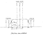
- Figure 1 illustrates how this mode of interference arises for f.m. signals.
- the carrier of the adjacent channel can fall within the receiver I.F. filter passband resulting in a baseband tone in the wanted channel.
- the frequency of this tone will be between 9.46MHz and 19MHz.
- Figure 2a shows the sideband structure of the wanted signal. It contains a multiplicity of sidebands. Most of the energy falls within the bandwidth of the receiver I.F. filter. The sidebands occur in pairs and their phase relative to carrier is 90°.
- Figure 2b shows the sideband structure of an unwanted signal.
- RX receiver
- I.F. filter bandwidth there will be a number of components within the RX bandwidth. These will generally fall on the same side of the receiver centre frequency as does the carrier of the interfering signal. Only a small amount of energy from the interfering signal will fall on the opposite side.
- German patent 1217464 suggests that noise affecting the output of an f.m. demodulator may be compensated by f.m. and a.m. demodulating the input f.m. signal and forming a weighted combination of the demodulated signals.
- the present invention utilises this fundamental difference to distinguish interference from the wanted signal so that the interfering sidebands may be separated from the desired signal and suppressed.
- a correction signal to be applied to an f.m. demodulated signal so as to reduce adjacent channel interference, is produced by processing a signal corresponding to the square of the envelope of the input signal.
- the correction signal is proportional to the frequency of the "square" signal.
- a correction signal may be produced by processing a signal corresponding to the amplitude variation of the input signal, rather than the square of the envelope.
- the effect of this correction signal is to significantly reduce the interfering harmonics as well as the fundamental, leading to a greater overall reduction in the power of the interfering signal.
- the present invention utilises a triangulator, i.e. a device which processes an input signal with a type of filtering function to produce an output the magnitude of which is a function of the frequency of the input signal.
- a triangulator is effectively equivalent to a differentiator but its output does not have the 90° phase shift possessed by the output of a differentiator.
- a disadvantage with the alternative technique mentioned above is that the a.m. demodulation step results in an addition of noise to the signal. This noise can he reduced if the cancellation process is applied over only a part of the signal.
- a filter step is included in the method to allow only a desired part of the signal to be passed for the cancellation process.
- the adjacent channel interference occurs mainly at the top of the video-baseband (i.e. at the higher frequencies), so, for such a video signal it is preferred to high pass filter the a.m. demodulated signal prior to cancellation with the f.m. demodulated signal. This has the advantage of reducing the amount of noise added to the interference cancelled signal by the a.m. demodulation step.
- the process can, in principle, completely eliminate interference from an adjacent channel to one side of the desired signal channel.
- interference is also occurring on the other side of the desired signal channel, (i.e. on the other side of the wanted carrier) problems arise, because there will be no phase reversal of the output from the a.m. demodulation step whereas phase reversal occurs at the f.m. demodulator output. Therefore it will be necessary to change the polarity of the a.m. demodulated signal in order to get correct cancellation of interference.
- the wanted carrier will be of a frequency which represents a grey level of picture.
- a variable gain stage controlled by the frequency of the f.m. demodulated signal can be used to produce a correction signal which will cancel interference on either side of the wanted carrier, the side being cancelled depending on the level of the f.m. demodulated signal. For example, when the wanted signal is approaching white, interference from the upper channel will be suppressed. When the wanted signal is approaching black, interference from the lower channel will be suppressed. And when the wanted signal is at mid-grey level there is no suppression of interference, however the level of interference from either side in this case may not be significant dependent upon factors such as channel spacing.
- the present invention can be used with vestigial sideband signals, such as vestigial sideband f.m. Vestigial sideband a.m. is currently used in the U.K. for PAL transmission.
- Vestigial sideband f.m. is envisaged for transmission of such signals as D-MAC over cable.
- a process in accordance with the present invention can advantageously be used to reconstruct the missing sideband, by adding the differentiated a.m. demodulated signal to the f.m. demodulated signal.
- the present invention provides a method for receiving a vestigial sideband signal comprising the steps of:
- the present invention further provides apparatus for receiving a vestigial sideband signal, comprising:
- a similar technique can also be used with advantage to cater for uplink interference in, for example, satellite broadcasting systems.
- Downlink interference occurs to the transmitted signal between the satellite and ground, and can be reduced in accordance with the interference suppression method of the present invention by cancelling the f.m. demodulated signal by the triangulated a.m. demodulated signal.
- the uplink interference (caused between ground and satellite) cannot be reduced by this technique, due to the non-linearity of the satellite transponder.
- the missing sideband may be reconstructed by adding the triangulated a.m. demodulated signal to the demodulated f.m. signal.
- This is one way of catering for uplink interference; it is also useful when a strong interfering signal affects one sideband only of the wanted signal.
- the present invention still further provides a method for receiving a wideband signal comprising the steps of:
- the present invention yet further provides apparatus for receiving a wideband signal, comprising:
- an f.m signal such as e.g. a MAC television signal ( ie , D MAC, HD MAC, W MAC etc).
- Figure 3b shows a vector representation of the wanted carrier with f.m modulation.
- the modulation sidebands A, B are represented by two counter rotating vectors.
- the resultant vector R changes phase but not amplitude.
- Figure 3a represents the wanted carrier plus an interfering sideband.
- the resultant vector R varies in both amplitude and phase. If this signal is subjected to both an f.m demodulation process and an a.m demodulation process, then a sine wave will be produced at both demodulator outputs.
- the signal from the a.m demodulator will be in phase with that from the f.m demodulator. Furthermore, if difference frequency between the wanted carrier and unwanted sideband is F, then the amplitude of the output from the a.m demodulator will be independent of F whereas that from the f.m demodulator will be linearly proportional to F.
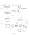
- Fig. 4a shows a method by which interference cancellation can be achieved for all values of F.
- the output from the a.m demodulator 1 is subjected to a triangulation process and then subtracted from the output of the f.m demodulator 2.
- the f.m demodulator output 3 passes through the summing node 4 uncorrupted, since there is no output from a.m demodulator 1.
- the gains of the f.m and a.m channel 6,7 can be set to achieve total rejection of that signal as seen at the final output 8.
- the improvement in interference performance is achieved at the expense of a signal to noise degradation. It can be shown that the contribution of noise from the a.m demodulator 1 is exactly the same as that from the f.m demodulator 2, resulting in a S/N ratio penalty of 3dB.
- the baseband interference occurs mainly at the top of the baseband, so the system is still effective if a high pass filter is included as in Figure 4b. (This is the block diagram of a preferred system). Typically, by this means, the noise penalty can be reduced to less than 1dB.
- a variable gain stage 16 is included as a means of controlling the phase 0°/180° and amplitude of the correction signal.
- Figure 4b shows another arrangement the output from the f.m demodulator 2 is low pass filtered 15 and then used as the control signal of a variable gain stage 16.
- the gain versus control voltage characteristic of the variable gain stage is typically as shown in Figure 6.
- Delay element T1 13 is necessary to guarantee that both the control signal 17 and input signal 18 to the variable gain stage, are timed correctly relative to each other.
- Delay element T2 12 is necessary to guarantee that the f.m and a.m components are timed correctly relative to each other at the output summing node 14.
- the uplink contribution will be normally substantially less than the downlink contribution so the system can provide an overall improvement.
- Vestigial sideband am transmission is currently used for PAL.
- Vestigial sideband fm has been proposed for cable transmission of DMAC.
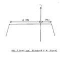
- Figure 7 illustrates the form of filtering proposed. It allows frequency components to about 10 Mhz below vision centre frequency, but only to about 3 MHz above.
- VSB transmission is that if a conventional f.m demodulator is used, then the baseband frequency response will be substantially non flat. Equalisation either at the transmitter or the receiver may improve this. In a TV system the non-flatness will be dependent on picture grey level, so accurate equalisation is difficult.
- the interference suppression technique of the present invention can be used as a means of reducing distortion in the demodulation of VSB f.m.
- the circuit of figure 4a modified so that the output for the triangulator is added to that for the f.m demodulator rather than being subtracted from it.
- the output from the d.m demod 3 will reduce by 6dB, but will be reinforced by the a.m demod output 3 to produce the correct overall result.
- this method could be used to remove uplink interference, by filtering the wideband signal so that it resembles the vestigial sideband signal (thereby effectively removing the uplink interference on that side). then reconstructing the missing sideband by using the above technique.
- the present invention has been described generally in terms of frequency modulated signals and particularly in terms of MAC television signals. It can be utilised for any f.m transmission, or even a.m transmission. It is not limited to satellite broadcasting, it can be used with any method of broadcasting, for example cable, MVDS, etc.
Landscapes
- Engineering & Computer Science (AREA)
- Power Engineering (AREA)
- Multimedia (AREA)
- Signal Processing (AREA)
- Noise Elimination (AREA)
Claims (6)
- Procédé de réception d'un signal à bande latérale atténuée comprenant les étapes :de réception, comme entrée, du signal à bande latérale atténuée ;de démodulation FM du signal d'entrée ;de démodulation AM du signal d'entrée ;de traitement du signal démodulé AM pour produire un signal supplémentaire dont l'amplitude est proportionnelle à la fréquence du signal démodulé AM ; etd'addition du signal supplémentaire au signal démodulé FM, le signal supplémentaire et le signal démodulé FM étant commandés pour être en phase avant d'être additionnés, pour compenser ainsi sensiblement la bande latérale atténuée, et de sortie du signal résultant.
- Procédé de réception d'un signal à large bande comprenant les étapes :de réception, comme entrée, du signal émis ;de filtrage du signal d'entrée pour éliminer sensiblement une bande latérale et le bruit associé ;de démodulation FM du signal filtré ;de démodulation AM du signal filtré ;de traitement du signal démodulé AM pour produire un signal supplémentaire dont l'amplitude est proportionnelle à la fréquence du signal démodulé AM ; etd'addition du signal supplémentaire au signal démodulé FM, le signal supplémentaire et le signal démodulé FM étant commandés pour être en phase avant d'être additionnés, pour compenser ainsi sensiblement la bande latérale éliminée, et de sortie du signal résultant.
- Procédé selon la revendication 1 ou 2, et comprenant l'étape de filtrage passe-haut du signal supplémentaire avant sa combinaison avec le signal démodulé FM.
- Appareil de réception d'un signal à bande latérale atténuée, comprenant :un moyen pour recevoir, comme entrée (5), le signal à bande latérale atténuée ;un moyen de démodulation FM (2) pour démoduler FM le signal d'entrée ;un moyen de démodulation AM (1) pour démoduler AM le signal d'entrée ;un moyen de traitement (11) pour traiter le signal démodulé AM pour produire un signal supplémentaire dont l'amplitude est proportionnelle à la fréquence du signal démodulé AM ; etun moyen de combinaison (4) pour additionner le signal supplémentaire au signal démodulé FM, le signal supplémentaire et le signal démodulé FM étant commandés pour être en phase avant d'être combinés, pour compenser ainsi sensiblement la bande latérale atténuée, et pour sortir le signal résultant.
- Appareil de réception d'un signal à large bande, comprenant :un moyen pour recevoir, comme entrée (5), le signal à large bande ;un moyen pour filtrer le signal d'entrée pour éliminer sensiblement une bande latérale et le bruit associé ;un moyen de démodulation FM (2) pour démoduler FM le signal d'entrée ;un moyen de démodulation AM (1) pour démoduler AM le signal d'entrée ;un moyen de traitement (11) pour traiter le signal démodulé AM (9) pour produire un signal supplémentaire dont l'amplitude est proportionnelle à la fréquence du signal démodulé AM ; etun moyen de combinaison pour additionner le signal supplémentaire (1) au signal démodulé FM (3), le signal supplémentaire et le signal démodulé FM étant commandés pour être en phase avant d'être combinés, pour compenser ainsi sensiblement la bande latérale éliminée, et pour sortir le signal résultant.
- Appareil selon la revendication 4 ou 5, et comprenant en outre un filtre passe-haut agencé pour opérer sur la sortie du moyen de traitement de signal démodulé AM.
Applications Claiming Priority (2)
| Application Number | Priority Date | Filing Date | Title |
|---|---|---|---|
| GB888818693A GB8818693D0 (en) | 1988-08-05 | 1988-08-05 | Interference suppression for transmitted signals & demodulation of vestigial sideband signals |
| GB8818693 | 1988-08-05 |
Publications (2)
| Publication Number | Publication Date |
|---|---|
| EP0356055A1 EP0356055A1 (fr) | 1990-02-28 |
| EP0356055B1 true EP0356055B1 (fr) | 1996-03-20 |
Family
ID=10641698
Family Applications (1)
| Application Number | Title | Priority Date | Filing Date |
|---|---|---|---|
| EP89307988A Expired - Lifetime EP0356055B1 (fr) | 1988-08-05 | 1989-08-04 | Suppression d'interférence pour signaux transmis et démodulation de signaux de bande résiduelle |
Country Status (8)
| Country | Link |
|---|---|
| EP (1) | EP0356055B1 (fr) |
| JP (1) | JPH04500143A (fr) |
| AT (1) | ATE135858T1 (fr) |
| AU (1) | AU4061389A (fr) |
| CA (1) | CA1308445C (fr) |
| DE (1) | DE68926004T2 (fr) |
| GB (1) | GB8818693D0 (fr) |
| WO (1) | WO1990001830A1 (fr) |
Families Citing this family (2)
| Publication number | Priority date | Publication date | Assignee | Title |
|---|---|---|---|---|
| FR2821500B1 (fr) * | 2001-02-26 | 2005-05-13 | St Microelectronics Sa | Procede et dispositif de compensation du decalage cc dynamique d'un recepteur a conversion directe |
| EP2056767A4 (fr) | 2006-08-29 | 2012-12-26 | Playtex Products Inc | Dispositif d'extraction de tampon hygiénique |
Family Cites Families (1)
| Publication number | Priority date | Publication date | Assignee | Title |
|---|---|---|---|---|
| DE1217464B (de) * | 1962-03-26 | 1966-05-26 | Johann Stegmueller | Schaltungsanordnung zur Kompensation einer von einer Amplitudenmodulation herruehrenden Stoerspannung in der Ausgangsspannung eines Demodulators fuer frequenzmodulierte,elektrische Hochfrequenzschwingungen |
-
1988
- 1988-08-05 GB GB888818693A patent/GB8818693D0/en active Pending
-
1989
- 1989-08-04 AU AU40613/89A patent/AU4061389A/en not_active Abandoned
- 1989-08-04 WO PCT/GB1989/000893 patent/WO1990001830A1/fr not_active Ceased
- 1989-08-04 CA CA000607596A patent/CA1308445C/fr not_active Expired - Lifetime
- 1989-08-04 EP EP89307988A patent/EP0356055B1/fr not_active Expired - Lifetime
- 1989-08-04 JP JP1508729A patent/JPH04500143A/ja active Pending
- 1989-08-04 AT AT89307988T patent/ATE135858T1/de not_active IP Right Cessation
- 1989-08-04 DE DE68926004T patent/DE68926004T2/de not_active Expired - Fee Related
Also Published As
| Publication number | Publication date |
|---|---|
| DE68926004D1 (de) | 1996-04-25 |
| EP0356055A1 (fr) | 1990-02-28 |
| HK1004764A1 (en) | 1998-12-04 |
| DE68926004T2 (de) | 1996-10-24 |
| WO1990001830A1 (fr) | 1990-02-22 |
| ATE135858T1 (de) | 1996-04-15 |
| AU4061389A (en) | 1990-03-05 |
| GB8818693D0 (en) | 1988-09-07 |
| CA1308445C (fr) | 1992-10-06 |
| JPH04500143A (ja) | 1992-01-09 |
Similar Documents
| Publication | Publication Date | Title |
|---|---|---|
| USRE36992E (en) | VSB HDTV transmission system with reduced NTSC co-channel interference | |
| US5162900A (en) | Co-channel interference filter for television receiver | |
| US5121203A (en) | HDTV transmission system with reduced NTSC CO-channel interference | |
| US5400084A (en) | Method and apparatus for NTSC signal interference cancellation using recursive digital notch filters | |
| AU662126B2 (en) | Modulator/demodulator for compatible high definition television system | |
| US4958230A (en) | Method of transmitting auxiliary information in a television signal | |
| KR100257475B1 (ko) | 디지탈 텔레비전 신호 수신기용 자동 이득 제어 장치 | |
| US5325188A (en) | Apparatus for NTSC signal interference cancellation through the use of digital recursive notch filters | |
| US5268761A (en) | Automatic gain control system for a high definition television signal receiver including an adaptive equalizer | |
| US5077542A (en) | Transmission system with suppressed carrier signal amplitude modulation preserving the polarity of the transmitted signal, and corresponding transmitter and receiver | |
| US5909253A (en) | Reducing video crosstalk in a data carrier located within a vestigial sideband of a standard television signal | |
| CA1227566A (fr) | Filtre a frequence intermediaire a correction de la modulation de phase de nyquist | |
| EP0356055B1 (fr) | Suppression d'interférence pour signaux transmis et démodulation de signaux de bande résiduelle | |
| US6400393B1 (en) | DTV receiver with filter in I-F circuitry to suppress FM sound carrier of NTSC Co-channel interfering signal | |
| US4513323A (en) | Buzz reduction for intercarrier type television sound detection | |
| US5027210A (en) | Noise reduction in high definition television signals | |
| US5258838A (en) | HDTV transmission system with reduced NTSC co-channel interference | |
| HK1004764B (en) | Interference suppression for transmitted signals and demodulation of vestigial sideband signals | |
| HK1004771B (en) | Noise reduction in television signals | |
| US5241538A (en) | Transmission apparatus | |
| JPS6346084A (ja) | テレビジヨン信号の伝送方式 | |
| CA2058559C (fr) | Filtre contre le brouillage co-canal pour recepteur de television | |
| EP0300801B1 (fr) | Appareil de démodulation de fréquence | |
| JPS62281685A (ja) | 高感度fm復調器 | |
| JPH02116227A (ja) | 伝送歪除去回路 |
Legal Events
| Date | Code | Title | Description |
|---|---|---|---|
| PUAI | Public reference made under article 153(3) epc to a published international application that has entered the european phase |
Free format text: ORIGINAL CODE: 0009012 |
|
| AK | Designated contracting states |
Kind code of ref document: A1 Designated state(s): AT BE CH DE ES FR GB GR IT LI LU NL SE |
|
| 17P | Request for examination filed |
Effective date: 19900412 |
|
| 17Q | First examination report despatched |
Effective date: 19901213 |
|
| GRAH | Despatch of communication of intention to grant a patent |
Free format text: ORIGINAL CODE: EPIDOS IGRA |
|
| RAP1 | Party data changed (applicant data changed or rights of an application transferred) |
Owner name: NATIONAL TRANSCOMMUNICATIONS LIMITED |
|
| GRAA | (expected) grant |
Free format text: ORIGINAL CODE: 0009210 |
|
| AK | Designated contracting states |
Kind code of ref document: B1 Designated state(s): AT BE CH DE ES FR GB GR IT LI LU NL SE |
|
| PG25 | Lapsed in a contracting state [announced via postgrant information from national office to epo] |
Ref country code: BE Effective date: 19960320 Ref country code: GR Free format text: LAPSE BECAUSE OF FAILURE TO SUBMIT A TRANSLATION OF THE DESCRIPTION OR TO PAY THE FEE WITHIN THE PRESCRIBED TIME-LIMIT Effective date: 19960320 Ref country code: LI Effective date: 19960320 Ref country code: AT Effective date: 19960320 Ref country code: CH Effective date: 19960320 Ref country code: ES Free format text: THE PATENT HAS BEEN ANNULLED BY A DECISION OF A NATIONAL AUTHORITY Effective date: 19960320 Ref country code: IT Free format text: LAPSE BECAUSE OF FAILURE TO SUBMIT A TRANSLATION OF THE DESCRIPTION OR TO PAY THE FEE WITHIN THE PRE;WARNING: LAPSES OF ITALIAN PATENTS WITH EFFECTIVE DATE BEFORE 2007 MAY HAVE OCCURRED AT ANY TIME BEFORE 2007. THE CORRECT EFFECTIVE DATE MAY BE DIFFERENT FROM THE ONE RECORDED.SCRIBED TIME-LIMIT Effective date: 19960320 |
|
| REF | Corresponds to: |
Ref document number: 135858 Country of ref document: AT Date of ref document: 19960415 Kind code of ref document: T |
|
| REF | Corresponds to: |
Ref document number: 68926004 Country of ref document: DE Date of ref document: 19960425 |
|
| RAP2 | Party data changed (patent owner data changed or rights of a patent transferred) |
Owner name: DIGI-MEDIA VISION LIMITED |
|
| PG25 | Lapsed in a contracting state [announced via postgrant information from national office to epo] |
Ref country code: SE Effective date: 19960620 |
|
| ET | Fr: translation filed | ||
| NLT2 | Nl: modifications (of names), taken from the european patent patent bulletin |
Owner name: DIGI-MEDIA VISION LIMITED |
|
| PG25 | Lapsed in a contracting state [announced via postgrant information from national office to epo] |
Ref country code: LU Free format text: LAPSE BECAUSE OF NON-PAYMENT OF DUE FEES Effective date: 19960831 |
|
| REG | Reference to a national code |
Ref country code: CH Ref legal event code: PL |
|
| NLXE | Nl: other communications concerning ep-patents (part 3 heading xe) |
Free format text: PAT.BUL.09/96 PAGE 1242:CORR.:DIGI-MEDIA VISION LIMITED |
|
| PLBE | No opposition filed within time limit |
Free format text: ORIGINAL CODE: 0009261 |
|
| STAA | Information on the status of an ep patent application or granted ep patent |
Free format text: STATUS: NO OPPOSITION FILED WITHIN TIME LIMIT |
|
| 26N | No opposition filed | ||
| PGFP | Annual fee paid to national office [announced via postgrant information from national office to epo] |
Ref country code: NL Payment date: 19990630 Year of fee payment: 11 |
|
| PGFP | Annual fee paid to national office [announced via postgrant information from national office to epo] |
Ref country code: GB Payment date: 19990702 Year of fee payment: 11 |
|
| PGFP | Annual fee paid to national office [announced via postgrant information from national office to epo] |
Ref country code: FR Payment date: 19990802 Year of fee payment: 11 |
|
| PGFP | Annual fee paid to national office [announced via postgrant information from national office to epo] |
Ref country code: DE Payment date: 19990831 Year of fee payment: 11 |
|
| REG | Reference to a national code |
Ref country code: GB Ref legal event code: 732E |
|
| PG25 | Lapsed in a contracting state [announced via postgrant information from national office to epo] |
Ref country code: GB Free format text: LAPSE BECAUSE OF NON-PAYMENT OF DUE FEES Effective date: 20000804 |
|
| PG25 | Lapsed in a contracting state [announced via postgrant information from national office to epo] |
Ref country code: NL Free format text: LAPSE BECAUSE OF NON-PAYMENT OF DUE FEES Effective date: 20010301 |
|
| GBPC | Gb: european patent ceased through non-payment of renewal fee |
Effective date: 20000804 |
|
| PG25 | Lapsed in a contracting state [announced via postgrant information from national office to epo] |
Ref country code: FR Free format text: LAPSE BECAUSE OF NON-PAYMENT OF DUE FEES Effective date: 20010430 |
|
| NLV4 | Nl: lapsed or anulled due to non-payment of the annual fee |
Effective date: 20010301 |
|
| PG25 | Lapsed in a contracting state [announced via postgrant information from national office to epo] |
Ref country code: DE Free format text: LAPSE BECAUSE OF NON-PAYMENT OF DUE FEES Effective date: 20010501 |
|
| REG | Reference to a national code |
Ref country code: FR Ref legal event code: ST |