EP0365874B1 - Système et méthode d'inspection optique des sondures - Google Patents
Système et méthode d'inspection optique des sondures Download PDFInfo
- Publication number
- EP0365874B1 EP0365874B1 EP89118302A EP89118302A EP0365874B1 EP 0365874 B1 EP0365874 B1 EP 0365874B1 EP 89118302 A EP89118302 A EP 89118302A EP 89118302 A EP89118302 A EP 89118302A EP 0365874 B1 EP0365874 B1 EP 0365874B1
- Authority
- EP
- European Patent Office
- Prior art keywords
- optical
- solder joint
- inspection
- solder
- lead
- Prior art date
- Legal status (The legal status is an assumption and is not a legal conclusion. Google has not performed a legal analysis and makes no representation as to the accuracy of the status listed.)
- Expired - Lifetime
Links
- 229910000679 solder Inorganic materials 0.000 title claims description 78
- 238000007689 inspection Methods 0.000 title claims description 49
- 230000003287 optical effect Effects 0.000 title claims description 31
- 238000000034 method Methods 0.000 title claims description 16
- 238000005286 illumination Methods 0.000 claims description 10
- 238000004458 analytical method Methods 0.000 claims description 5
- 230000002463 transducing effect Effects 0.000 claims description 2
- 239000000835 fiber Substances 0.000 description 5
- 238000005476 soldering Methods 0.000 description 4
- 238000011179 visual inspection Methods 0.000 description 4
- 230000000007 visual effect Effects 0.000 description 3
- 230000007547 defect Effects 0.000 description 2
- 238000003908 quality control method Methods 0.000 description 2
- 230000004304 visual acuity Effects 0.000 description 2
- RYGMFSIKBFXOCR-UHFFFAOYSA-N Copper Chemical compound [Cu] RYGMFSIKBFXOCR-UHFFFAOYSA-N 0.000 description 1
- 206010052128 Glare Diseases 0.000 description 1
- 241000519995 Stachys sylvatica Species 0.000 description 1
- 238000004140 cleaning Methods 0.000 description 1
- 239000003086 colorant Substances 0.000 description 1
- 238000011109 contamination Methods 0.000 description 1
- 229910052802 copper Inorganic materials 0.000 description 1
- 239000010949 copper Substances 0.000 description 1
- 230000002950 deficient Effects 0.000 description 1
- 238000010586 diagram Methods 0.000 description 1
- 230000000694 effects Effects 0.000 description 1
- 238000011156 evaluation Methods 0.000 description 1
- 230000004313 glare Effects 0.000 description 1
- 208000013409 limited attention Diseases 0.000 description 1
- 239000000155 melt Substances 0.000 description 1
- 230000000737 periodic effect Effects 0.000 description 1
- 238000007747 plating Methods 0.000 description 1
Images


Classifications
-
- G—PHYSICS
- G01—MEASURING; TESTING
- G01R—MEASURING ELECTRIC VARIABLES; MEASURING MAGNETIC VARIABLES
- G01R31/00—Arrangements for testing electric properties; Arrangements for locating electric faults; Arrangements for electrical testing characterised by what is being tested not provided for elsewhere
- G01R31/28—Testing of electronic circuits, e.g. by signal tracer
- G01R31/302—Contactless testing
- G01R31/308—Contactless testing using non-ionising electromagnetic radiation, e.g. optical radiation
- G01R31/309—Contactless testing using non-ionising electromagnetic radiation, e.g. optical radiation of printed or hybrid circuits or circuit substrates
-
- G—PHYSICS
- G01—MEASURING; TESTING
- G01N—INVESTIGATING OR ANALYSING MATERIALS BY DETERMINING THEIR CHEMICAL OR PHYSICAL PROPERTIES
- G01N21/00—Investigating or analysing materials by the use of optical means, i.e. using sub-millimetre waves, infrared, visible or ultraviolet light
- G01N21/84—Systems specially adapted for particular applications
- G01N21/88—Investigating the presence of flaws or contamination
- G01N21/95—Investigating the presence of flaws or contamination characterised by the material or shape of the object to be examined
- G01N21/956—Inspecting patterns on the surface of objects
- G01N21/95684—Patterns showing highly reflecting parts, e.g. metallic elements
-
- G—PHYSICS
- G01—MEASURING; TESTING
- G01N—INVESTIGATING OR ANALYSING MATERIALS BY DETERMINING THEIR CHEMICAL OR PHYSICAL PROPERTIES
- G01N21/00—Investigating or analysing materials by the use of optical means, i.e. using sub-millimetre waves, infrared, visible or ultraviolet light
- G01N21/84—Systems specially adapted for particular applications
- G01N21/88—Investigating the presence of flaws or contamination
- G01N21/95—Investigating the presence of flaws or contamination characterised by the material or shape of the object to be examined
- G01N21/956—Inspecting patterns on the surface of objects
- G01N2021/95638—Inspecting patterns on the surface of objects for PCB's
- G01N2021/95646—Soldering
Definitions
- Stand 28 supports video camera 30 above the lead.
- the lens 32 of the video camera defines the axis at the center of the video field.
- the X-Y platform 14 moves the lead 22 onto the axis for video observation. Illumination is provided by a lamp which provides low angle diffuse illumination all around the area being inspected. Circular fluorescent lamp 34 is preferred. A high intensity, small diameter lamp is required. It provides light at a low angle with respect to the top of the printed wiring board 16 by being positioned as low as possible closely over the printed wiring board 16 as clearances permit.
- a specific example of a suitable light is a 3-1/2 inch (8,89 cm) diameter, 40 watt "Light Mite" circular high intensity fluorescent lamp.
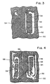
- the analyzer accepts or rejects the solder joint on the basis of satisfying one rule, which requires fillet along a Predetermined portion of the length of the lead. In commercial work, a 60 percent continuity of fillet is adequate. In high reliability work, a higher continuity is required. The absence of reflection from a significant length of the fillet indicates the inadequacy of fillet, and thus indicates the absence of a proper solder joint.
Landscapes
- Physics & Mathematics (AREA)
- General Physics & Mathematics (AREA)
- Health & Medical Sciences (AREA)
- Engineering & Computer Science (AREA)
- Life Sciences & Earth Sciences (AREA)
- Biochemistry (AREA)
- General Engineering & Computer Science (AREA)
- Electromagnetism (AREA)
- Computer Vision & Pattern Recognition (AREA)
- Chemical & Material Sciences (AREA)
- Analytical Chemistry (AREA)
- Toxicology (AREA)
- General Health & Medical Sciences (AREA)
- Immunology (AREA)
- Pathology (AREA)
- Investigating Materials By The Use Of Optical Means Adapted For Particular Applications (AREA)
- Length Measuring Devices By Optical Means (AREA)
- Closed-Circuit Television Systems (AREA)
Claims (6)
- Système d'inspection optique comportant :- des moyens de support (12, 14) pour le positionnement d'une plaquette (16 ; 50) à câblage imprimé portant des composants (20) montés en surface pourvus de joints soudés ;- un transducteur opto-électronique (30, 32) définissant un axe d'inspection normal par rapport auxdits moyens (12, 14) de support et positionné de façon à recevoir une image optique d'un joint soudé le long dudit axe d'inspection et conçu pour convertir ladite image optique du joint soudé en un signal d'image électronique ;- une source de lumière placée entre ladite plaquette (16 ; 50) à câblage imprimé et ledit transducteur opto-électronique (30, 32) pour éclairer ledit joint soudé par rapport audit axe d'inspection de manière que de la lumière provenant de ladite source de lumière tombe sur des surfaces plates (52, 54, 56) de ladite plaquette (16 ; 50) et de conducteurs allongés (22) de composants, respectivement, sous un petit angle par rapport auxdites surfaces plates (52, 54, 56) afin d'empêcher une réflexion à partir de celles-ci dans ledit transducteur opto-électronique (30, 32), alors que de la lumière provenant de ladite source de lumière et tombant sur des surfaces concaves de congés (24, 26) de joints soudés contiguës auxdits conducteurs allongés (22) de composants, est réfléchie dans ledit transducteur opto-électronique (30, 32), engendrant ainsi ladite image optique de joint soudé avec les zones sombres représentant les surfaces plates (52, 54, 56) et des bandes claires (58, 60) représentant lesdites surfaces concaves des congés ;- des moyens (38) destinés à numériser ledit signal d'image électronique et à le convertir en une information numérisée ;- des moyens (38) destinés à analyser ladite information numérisée pour évaluer la qualité dudit joint soudé, lesdits moyens d'analyse (38) étant contigus de façon à détecter l'état complet desdites bandes (58, 60) le long desdits conducteurs (22) de composants ; et- des moyens à signal d'achèvement générant un signal d'achèvement et d'acceptation lorsque ledit état complet correspond à une bande continue le long d'une proportion prédéterminée de la longueur totale du congé.
- Système selon la revendication 1, caractérisé en ce que ladite source de lumière est une lampe circulaire (34) à fluorescence, à haute intensité, faible diamètre, placée autour dudit axe.
- Système selon la revendication 2, caractérisé en ce que ladite lampe circulaire (34) à fluorescence est placée étroitement au-dessus desdits moyens (12, 14) de support pour produire un éclairage diffusant sous un petit angle pratiquement tout autour dudit axe.
- Système selon l'une quelconque des revendications 1 à 3, caractérisé en ce que lesdits moyens de support comprennent une table (12, 14) de positionnement et en ce que lesdits moyens d'analyse (38) sont connectés à ladite table (12, 14) de positionnement de manière que, lorsque l'analyse d'un joint soudé est achevée, ladite table (12, 14) de positionnement, à la suite de l'apparition du signal d'achèvement et d'acceptation, se déplace jusqu'à une position dans laquelle un nouveau plot (18) et son conducteur (22) de composant se trouvent sur ledit axe.
- Procédé d'inspection optique d'un joint soudé, comprenant les étapes qui consistent :- à positionner sur un axe d'inspection et normalement à celui-ci une plaquette (16 ; 50) à câblage imprimé portant un plot (18) avec un conducteur (22) de composant sur ledit plot (18) soudé à dessein audit plot (18) au moyen de congés (24, 26) de soudure s'étendant le long dudit conducteur (22) entre ledit plot (18) et ledit conducteur (22), ladite plaquette (16 ; 50) à câblage imprimé et ledit conducteur (22) ayant des surfaces plates (52, 54, 56) alors que lesdits congés (24, 26) ont des surfaces concaves ;- à positionner une lampe (34) pour appliquer de la lumière sous un petit angle sur ledit plot (18) afin qu'une réflexion à partir desdites surfaces plates (52, 54, 56) de ladite plaquette (16 ; 50) à câblage imprimé et dudit conducteur (22) ne se réfléchisse pas directement sur ledit axe optique, alors qu'une réflexion provenant desdits congés (24, 26) de soudure, se réfléchisse sur ledit axe optique, engendrant ainsi une image optique du joint soudé avec des zones sombres représentant lesdites surfaces plates (52, 54, 56) et des bandes claires (58, 60) représentant lesdites surfaces concaves des congés ;- à traduire ladite image optique en une information optique numérique ;- à analyser ladite information optique numérisée pour évaluer la qualité dudit joint soudé en détectant l'état achevé desdites bandes (58, 60) le long desdits conducteurs (22) de composants ;- à générer un signal d'achèvement et d'acceptation lorsque ledit état achevé correspond à une bande continue le long d'une proportion prédéterminée de la longueur totale du congé.
- Procédé selon la revendication 5, caractérisé en ce qu'il consiste à repositionner ladite plaquette (16 ; 50) à câblage imprimé après que le signal d'achèvement et d'acceptation a été produit pour placer un nouveau plot (18) pour une inspection optique.
Applications Claiming Priority (2)
| Application Number | Priority Date | Filing Date | Title |
|---|---|---|---|
| US25247688A | 1988-10-03 | 1988-10-03 | |
| US252476 | 2002-09-23 |
Publications (2)
| Publication Number | Publication Date |
|---|---|
| EP0365874A1 EP0365874A1 (fr) | 1990-05-02 |
| EP0365874B1 true EP0365874B1 (fr) | 1993-07-21 |
Family
ID=22956169
Family Applications (1)
| Application Number | Title | Priority Date | Filing Date |
|---|---|---|---|
| EP89118302A Expired - Lifetime EP0365874B1 (fr) | 1988-10-03 | 1989-10-03 | Système et méthode d'inspection optique des sondures |
Country Status (7)
| Country | Link |
|---|---|
| EP (1) | EP0365874B1 (fr) |
| JP (1) | JPH02249957A (fr) |
| AU (1) | AU608175B2 (fr) |
| CA (1) | CA1318414C (fr) |
| DE (1) | DE68907688T2 (fr) |
| ES (1) | ES2042923T3 (fr) |
| IL (1) | IL91492A (fr) |
Families Citing this family (9)
| Publication number | Priority date | Publication date | Assignee | Title |
|---|---|---|---|---|
| NO914574L (no) * | 1991-11-22 | 1993-05-24 | Elkem Technology | Fremgangsmaate for detektering av pin-hull i strengestoeptemetallemne |
| US5828449A (en) * | 1997-02-26 | 1998-10-27 | Acuity Imaging, Llc | Ring illumination reflective elements on a generally planar surface |
| US5926557A (en) * | 1997-02-26 | 1999-07-20 | Acuity Imaging, Llc | Inspection method |
| JP2007530962A (ja) * | 2004-03-27 | 2007-11-01 | テクスマーク ゲゼルシャフト ミット ベシュレンクテル ハフツング フェアトリーブスゲゼルシャフト | ラバーシート内の結合部を検出するための装置 |
| DE102009017695B3 (de) | 2009-04-15 | 2010-11-25 | Göpel electronic GmbH | Verfahren zur Inspektion von Lötstellen an elektrischen und elektronischen Bauteilen |
| CN105866657A (zh) * | 2016-03-25 | 2016-08-17 | 航天科技控股集团股份有限公司 | 自动检测印制板的针床和自动检测控制方法 |
| CN111307812A (zh) * | 2019-03-05 | 2020-06-19 | 南昌工程学院 | 基于机器视觉的焊点外观检测方法 |
| CN112344879B (zh) * | 2020-09-29 | 2022-03-25 | 联想(北京)有限公司 | 一种胶路的检测方法、装置及设备 |
| CN116967664A (zh) * | 2023-07-27 | 2023-10-31 | 深圳市世宗自动化设备有限公司 | 焊接补焊方法、装置及电子设备 |
Family Cites Families (5)
| Publication number | Priority date | Publication date | Assignee | Title |
|---|---|---|---|---|
| US4152723A (en) * | 1977-12-19 | 1979-05-01 | Sperry Rand Corporation | Method of inspecting circuit boards and apparatus therefor |
| US4538909A (en) * | 1983-05-24 | 1985-09-03 | Automation Engineering, Inc. | Circuit board inspection apparatus and method |
| JPS61293657A (ja) * | 1985-06-21 | 1986-12-24 | Matsushita Electric Works Ltd | 半田付け外観検査方法 |
| US4672437A (en) * | 1985-07-08 | 1987-06-09 | Honeywell Inc. | Fiber optic inspection system |
| EP0236738A3 (fr) * | 1986-02-05 | 1988-12-21 | OMRON Corporation | Procédé d'entrée de dates d'une plaque à circuits imprimés équipée de référence pour le traitement d'images d'un appareil d'inspection automatique de plaques à circuits imprimés équipées |
-
1989
- 1989-08-31 IL IL9149289A patent/IL91492A/en not_active IP Right Cessation
- 1989-09-15 AU AU41436/89A patent/AU608175B2/en not_active Ceased
- 1989-09-20 CA CA000612093A patent/CA1318414C/fr not_active Expired - Fee Related
- 1989-10-03 JP JP1258637A patent/JPH02249957A/ja active Pending
- 1989-10-03 ES ES89118302T patent/ES2042923T3/es not_active Expired - Lifetime
- 1989-10-03 DE DE89118302T patent/DE68907688T2/de not_active Expired - Fee Related
- 1989-10-03 EP EP89118302A patent/EP0365874B1/fr not_active Expired - Lifetime
Also Published As
| Publication number | Publication date |
|---|---|
| EP0365874A1 (fr) | 1990-05-02 |
| IL91492A0 (en) | 1990-04-29 |
| IL91492A (en) | 1994-07-31 |
| AU4143689A (en) | 1990-04-05 |
| ES2042923T3 (es) | 1993-12-16 |
| DE68907688T2 (de) | 1993-10-28 |
| AU608175B2 (en) | 1991-03-21 |
| DE68907688D1 (de) | 1993-08-26 |
| CA1318414C (fr) | 1993-05-25 |
| JPH02249957A (ja) | 1990-10-05 |
Similar Documents
| Publication | Publication Date | Title |
|---|---|---|
| US5247344A (en) | Optical inspection system for solder joints and inspection method | |
| JP2510545B2 (ja) | 製品を検査する方法と装置 | |
| US5245421A (en) | Apparatus for inspecting printed circuit boards with surface mounted components | |
| US5058178A (en) | Method and apparatus for inspection of specular, three-dimensional features | |
| US5302836A (en) | High speed image acquisition for microelectronics inspection | |
| US6084663A (en) | Method and an apparatus for inspection of a printed circuit board assembly | |
| JPH055281B2 (fr) | ||
| JP2009168582A (ja) | 外観検査装置 | |
| JPH0521403B2 (fr) | ||
| EP0341806B1 (fr) | Appareil pour l'inspection des plaques à cicuits imprimé aux composants montés sur la surface | |
| AU608175B2 (en) | Optical inspection system for solder joints and inspection methods | |
| JPH0875429A (ja) | ボンディングワイヤ検査方法 | |
| US7664311B2 (en) | Component mounting board inspecting apparatus | |
| EP0871027A2 (fr) | ContrÔle de plaques de circuits imprimés | |
| JPH05272939A (ja) | 圧着端子画像処理検査における照明方法及び画像処理方法 | |
| JPH063124A (ja) | ワイヤーボンディング外観検査装置 | |
| JPH04329344A (ja) | 実装基板検査装置 | |
| JP3162872B2 (ja) | 電子部品の輪郭認識装置及びその輪郭認識方法 | |
| JP3366211B2 (ja) | 鏡面対象物の撮像方式 | |
| JPH10227745A (ja) | リベット状部品の頭部側面検査方法およびその装置 | |
| JP3038107B2 (ja) | はんだ付け検査方法 | |
| JPH08285548A (ja) | バンプ外観検査装置 | |
| JPS6025405A (ja) | 半田面映像の入力方式 | |
| JP2981510B2 (ja) | リード部品検査装置 | |
| JPH0221244A (ja) | 半田ボールの検出方法 |
Legal Events
| Date | Code | Title | Description |
|---|---|---|---|
| PUAI | Public reference made under article 153(3) epc to a published international application that has entered the european phase |
Free format text: ORIGINAL CODE: 0009012 |
|
| 17P | Request for examination filed |
Effective date: 19891026 |
|
| AK | Designated contracting states |
Kind code of ref document: A1 Designated state(s): CH DE ES FR GB IT LI SE |
|
| 17Q | First examination report despatched |
Effective date: 19910510 |
|
| GRAA | (expected) grant |
Free format text: ORIGINAL CODE: 0009210 |
|
| ITF | It: translation for a ep patent filed | ||
| AK | Designated contracting states |
Kind code of ref document: B1 Designated state(s): CH DE ES FR GB IT LI SE |
|
| REF | Corresponds to: |
Ref document number: 68907688 Country of ref document: DE Date of ref document: 19930826 |
|
| ET | Fr: translation filed | ||
| REG | Reference to a national code |
Ref country code: ES Ref legal event code: FG2A Ref document number: 2042923 Country of ref document: ES Kind code of ref document: T3 |
|
| PLBE | No opposition filed within time limit |
Free format text: ORIGINAL CODE: 0009261 |
|
| STAA | Information on the status of an ep patent application or granted ep patent |
Free format text: STATUS: NO OPPOSITION FILED WITHIN TIME LIMIT |
|
| 26N | No opposition filed | ||
| PGFP | Annual fee paid to national office [announced via postgrant information from national office to epo] |
Ref country code: FR Payment date: 19940912 Year of fee payment: 6 |
|
| PGFP | Annual fee paid to national office [announced via postgrant information from national office to epo] |
Ref country code: GB Payment date: 19940914 Year of fee payment: 6 |
|
| PGFP | Annual fee paid to national office [announced via postgrant information from national office to epo] |
Ref country code: SE Payment date: 19940916 Year of fee payment: 6 |
|
| PGFP | Annual fee paid to national office [announced via postgrant information from national office to epo] |
Ref country code: DE Payment date: 19940919 Year of fee payment: 6 Ref country code: CH Payment date: 19940919 Year of fee payment: 6 |
|
| PGFP | Annual fee paid to national office [announced via postgrant information from national office to epo] |
Ref country code: ES Payment date: 19941007 Year of fee payment: 6 |
|
| EAL | Se: european patent in force in sweden |
Ref document number: 89118302.2 |
|
| PG25 | Lapsed in a contracting state [announced via postgrant information from national office to epo] |
Ref country code: GB Effective date: 19951003 |
|
| PG25 | Lapsed in a contracting state [announced via postgrant information from national office to epo] |
Ref country code: SE Effective date: 19951004 Ref country code: ES Free format text: LAPSE BECAUSE OF NON-PAYMENT OF DUE FEES Effective date: 19951004 |
|
| PG25 | Lapsed in a contracting state [announced via postgrant information from national office to epo] |
Ref country code: LI Effective date: 19951031 Ref country code: CH Effective date: 19951031 |
|
| GBPC | Gb: european patent ceased through non-payment of renewal fee |
Effective date: 19951003 |
|
| REG | Reference to a national code |
Ref country code: CH Ref legal event code: PL |
|
| PG25 | Lapsed in a contracting state [announced via postgrant information from national office to epo] |
Ref country code: FR Effective date: 19960628 |
|
| EUG | Se: european patent has lapsed |
Ref document number: 89118302.2 |
|
| PG25 | Lapsed in a contracting state [announced via postgrant information from national office to epo] |
Ref country code: DE Effective date: 19960702 |
|
| REG | Reference to a national code |
Ref country code: FR Ref legal event code: ST |
|
| REG | Reference to a national code |
Ref country code: ES Ref legal event code: FD2A Effective date: 19990503 |
|
| PG25 | Lapsed in a contracting state [announced via postgrant information from national office to epo] |
Ref country code: IT Free format text: LAPSE BECAUSE OF NON-PAYMENT OF DUE FEES Effective date: 20051003 |