EP0366799A1 - Stromversorgung für elektrische erosionsbearbeitung - Google Patents
Stromversorgung für elektrische erosionsbearbeitung Download PDFInfo
- Publication number
- EP0366799A1 EP0366799A1 EP89902068A EP89902068A EP0366799A1 EP 0366799 A1 EP0366799 A1 EP 0366799A1 EP 89902068 A EP89902068 A EP 89902068A EP 89902068 A EP89902068 A EP 89902068A EP 0366799 A1 EP0366799 A1 EP 0366799A1
- Authority
- EP
- European Patent Office
- Prior art keywords
- power source
- voltage
- capacitor
- electric
- discharge
- Prior art date
- Legal status (The legal status is an assumption and is not a legal conclusion. Google has not performed a legal analysis and makes no representation as to the accuracy of the status listed.)
- Granted
Links
- 238000003754 machining Methods 0.000 title claims abstract description 41
- 239000003990 capacitor Substances 0.000 claims abstract description 38
- 238000009499 grossing Methods 0.000 abstract description 7
- 238000010892 electric spark Methods 0.000 abstract 1
- 238000010586 diagram Methods 0.000 description 3
- 230000007423 decrease Effects 0.000 description 2
- 230000003247 decreasing effect Effects 0.000 description 2
- WABPQHHGFIMREM-UHFFFAOYSA-N lead(0) Chemical compound [Pb] WABPQHHGFIMREM-UHFFFAOYSA-N 0.000 description 2
Images

Classifications
-
- B—PERFORMING OPERATIONS; TRANSPORTING
- B23—MACHINE TOOLS; METAL-WORKING NOT OTHERWISE PROVIDED FOR
- B23H—WORKING OF METAL BY THE ACTION OF A HIGH CONCENTRATION OF ELECTRIC CURRENT ON A WORKPIECE USING AN ELECTRODE WHICH TAKES THE PLACE OF A TOOL; SUCH WORKING COMBINED WITH OTHER FORMS OF WORKING OF METAL
- B23H1/00—Electrical discharge machining, i.e. removing metal with a series of rapidly recurring electrical discharges between an electrode and a workpiece in the presence of a fluid dielectric
- B23H1/02—Electric circuits specially adapted therefor, e.g. power supply, control, preventing short circuits or other abnormal discharges
-
- B—PERFORMING OPERATIONS; TRANSPORTING
- B23—MACHINE TOOLS; METAL-WORKING NOT OTHERWISE PROVIDED FOR
- B23H—WORKING OF METAL BY THE ACTION OF A HIGH CONCENTRATION OF ELECTRIC CURRENT ON A WORKPIECE USING AN ELECTRODE WHICH TAKES THE PLACE OF A TOOL; SUCH WORKING COMBINED WITH OTHER FORMS OF WORKING OF METAL
- B23H1/00—Electrical discharge machining, i.e. removing metal with a series of rapidly recurring electrical discharges between an electrode and a workpiece in the presence of a fluid dielectric
- B23H1/02—Electric circuits specially adapted therefor, e.g. power supply, control, preventing short circuits or other abnormal discharges
- B23H1/022—Electric circuits specially adapted therefor, e.g. power supply, control, preventing short circuits or other abnormal discharges for shaping the discharge pulse train
-
- B—PERFORMING OPERATIONS; TRANSPORTING
- B23—MACHINE TOOLS; METAL-WORKING NOT OTHERWISE PROVIDED FOR
- B23H—WORKING OF METAL BY THE ACTION OF A HIGH CONCENTRATION OF ELECTRIC CURRENT ON A WORKPIECE USING AN ELECTRODE WHICH TAKES THE PLACE OF A TOOL; SUCH WORKING COMBINED WITH OTHER FORMS OF WORKING OF METAL
- B23H2300/00—Power source circuits or energization
- B23H2300/20—Relaxation circuit power supplies for supplying the machining current, e.g. capacitor or inductance energy storage circuits
Definitions
- the present invention relates to an electric-discharge-machining power source for use in an electric discharge machine, and more particularly, to a transistor type electric-discharge-machining power source which is capable of increasing a machining speed.
- machining pulses which are large in peak value but small in pulse width.
- a capacitor type electric-discharge-machining power source is employed so as to generate machining pulses which satisfy the aforementioned requirement.
- a transistor type electric-discharge-machining power source is also employed, which has an electric current return circuit for protecting a transistor from a surge current which is generated attributable to energy, accumulated in a stray inductance in a discharge circuit of the electric-discharge-machining power source, when the transistor is turned off.
- the object of the present invention is to provide an electric-discharge-machining power source in an electric discharge machine, which is capable of generating machining pulses having a large peak value and a small pulse width, thereby attaining an improved machining speed.
- an electric-discharge-machining power source of the present invention comprises: electric power source means; switching means for permitting and prohibiting an application of an electric power voltage from the electric power source means in between a workpiece and a tool electrode; a capacitor arranged to be charged up to a voltage beyond the electric power voltage; and a return circuit for returning a return electric current to the capacitor to charge the same capacitor, the return electric current being generated due to presence of a stray inductance of a discharge circuit when the application of the electric power voltage is prohibited by the switching means.
- a return electric current which is generated due to the presence of energy accumulated in the stray inductance of the discharge circuit of the electric-discharge-machining power source when the application of the electric power voltage in between the workpiece and the tool electrode is prohibited by the switching means, is returned to the capacitor so as to charge the same capacitor up to a voltage beyond the electric power voltage. Accordingly, it is possible to cause a return electric current to fall rapidly, to thereby generate machining pulses having a large peak value and a small pulse width, so that an improved machining speed is attained.
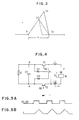
- a machining power source shown in Fig. 4 comprises transistors Tl and T2 each having a base to which a common pulse train G1, G2 (Fig. 5A) is applied.
- a voltage VO across terminals of an electric power source E is applied in between a workpiece W and a tool electrode P so that an electric discharge occurs therebetween, accompanied with generation of an electric discharge current i.
- the differential value of the electric discharge current i with respect to time is represented by the following equation (1), in other words, the electric discharge current i increases linearly with elapse of time, as shown in Fig. 5B.
- VG represents a gap voltage between the workpiece W and the electrode £
- L1, L2 each represent a stray inductance of a discharge circuit of the electric-discharge-machining power source, respectively.
- a machining pulse is generated, which is triangle in waveform which assumes a peak value upon the transistors being turned OFF and is symmetric with respect to the point of time at which the peak value appears.
- the electric-discharge-machining power source is basically constructed in the same manner as the arrangement of Fig. 4. That is, the electric-discharge-machining power source comprises an electric power source E and a capacitor C1 connected in parallel therewith for smoothing the power source voltage.
- the power source E has its positive terminal connected to the workpiece W through a transistor T2, and its negative terminal connected to the tool electrode P through a transistor T1 which cooperates with another transistor T2 to form switching means.
- These transistors T1, T2 each have a base supplied from a control circuit (not shown) with a pulse train G1, G2 for control of a transistor ON-OFF operation.
- a diode D1 for electric current return has its anode connected to a lead wire which connects the negative terminal of the power source E with the emitter of the transistor T1. Further, the anode of an electric current returning diode D2 is connected to another lead wire which connects the collector of the transistor T1 with the electrode f.
- reference symbols L1, L2 represent stray inductances of a discharge circuit of the electric-discharge-machining power source, and V0, VG represent the power source voltage and the gap voltage, respectively.
- Reference symbol C2 indicates a high-voltage smoothing capacitor having one end connected to the negative terminal of the power source E and another end connected to the cathode of the diode D2.
- a voltage divider consisting of resistors R1, R2 whose junction is connected to one input terminal of a comparator 1 having another input terminal to which a reference voltage VL is applied.
- An output terminal of the comparator 1 is connected to the base of a transistor T3 which serves as a second switching means, and which has the collector connected to a junction of the capacitor C2 and the resistor Rl and the emitter connected to the positive terminal of the power source E through an impedance Z.
- Reference symbol D3 indicates a fly-wheel diode connected in parallel with a coil, in case that the same coil forms the just- mentioned impedance Z.
- the transistors Tl, T2 In response to the control pulse trains Gl, G2 applied from the control circuit (not shown) to the bases of the transistors Tl, T2, these transistors are repetitively turned ON and OFF.
- the power source voltage VO is applied through the transistors to the gap between the workpiece W and the electrode P.
- the electric discharge current il Upon generation of electric discharge between the workpiece and the electrode, the electric discharge current il, represented by the following equation (3) corresponding to equation (1), flows along a path directing from the positive terminal of the power source E to the negative terminal thereof through the transistor T2, workpiece W, electrode P and transistor Tl. As shown in Fig. 2B, the discharge current il increases linearly with elapse of time.
- a return electric current i2 is generated attributable to energy accumulated in the stray inductances L1, L2, and flows along a path directing from one end of the high-voltage smoothing capacitor C2, connected to the negative terminal of the power source E, to the other end thereof through the diode Dl, workpiece W, electrode P and diode D2, so as to charge the capacitor C2.
- This return electric current i2 i.e., the discharge electric current in a state where the transistors Tl, T2 are turned OFF
- VC represents the voltage across the capacitor C2.
- the capacitor C2 is rapidly charged by the return electric current i2 up to the charge voltage VC beyond the power source voltage V0.
- the differential value di2/dt of the return electric current i.e., the discharge electric current upon the transistors being turned OFF
- equation (4) is larger than the differential value dil/dt of the discharge current when the transistors are turned ON, in other words, the fall of the return electric current i2 is steeper than the rise of the discharge current il (Figs. 2B and 2C).
- the comparator 1 is supplied at its one input terminal with a divided voltage VH, corresponding to the charge voltage VC of the capacitor, from the voltage divider.
- the transistor T3 is supplied at its base with a High-level output signal G3 (Fig. 2F) from the comparator 1, and is rendered to be conductive, whereby the return electric current i2 flows along a path directing from one end of the power- source-voltage smoothing capacitor Cl to the other end thereof through the diode D1, workpiece W, electrode P, diode D2, transistor T3 and impedance Z, so as to charge the capacitor Cl.
- the electric charge accumulated in the capacitor C2 is returned to the capacitor Cl through the transistor T3 and the impedance Z, so as to prevent an excessive increase in the charge voltage of the capacitor C2.
- the arrangement of the embodiment is common to the conventional arrangement in that the electric discharge current increases during a first time period starting at that point of time tl at which the transistor is turned ON to start the generation of the discharge current and ending at that point of time at which the transistor is turned OFF and the dicharge current has its peak value, and decreastw during a second time period starting at that time at which the transistor is turned OFF and ending at that point of time t2 at which the generation of the electric discharge current is terminated.
- the discharge current rapidly falls as shown by a solid line in Rig.
- the second time period (return-current generation time period) is considerably smaller than the first time period, as distinct from the case of the conventional arrangement wherein the discharge current falls as shown by a dotted line in Fig. 3 so that the first and second time periods are substantially equal to each other. Accordingly, If the pulsive discharge current having the same pulse width of JL is generated, the peak value Ip of the discharge current in the arrangement according to the embodiment is larger than the peak value Ip' in the conventional arrangement. If the generated discharge current has the same peak value, the pulse width of the discharge current in the apparatus of the embodiment is shorter than that in the conventional apparatus.
- a pulsive discharge current which has a regular pulse width and a regular peak value, can be attained by the use of a control circuit of a type disclosed, e.g., in Japanese Patent Publication No. 44-13195 from which pulse trains G1, G2 having a reduced variation in pulse width during the electric discharge machining are supplied.
Landscapes
- Engineering & Computer Science (AREA)
- Mechanical Engineering (AREA)
- Electrical Discharge Machining, Electrochemical Machining, And Combined Machining (AREA)
Applications Claiming Priority (2)
| Application Number | Priority Date | Filing Date | Title |
|---|---|---|---|
| JP63022906A JP2652392B2 (ja) | 1988-02-04 | 1988-02-04 | 放電加工電源 |
| JP22906/88 | 1988-02-04 |
Publications (3)
| Publication Number | Publication Date |
|---|---|
| EP0366799A1 true EP0366799A1 (de) | 1990-05-09 |
| EP0366799A4 EP0366799A4 (de) | 1990-05-14 |
| EP0366799B1 EP0366799B1 (de) | 1993-05-19 |
Family
ID=12095682
Family Applications (1)
| Application Number | Title | Priority Date | Filing Date |
|---|---|---|---|
| EP89902068A Expired - Lifetime EP0366799B1 (de) | 1988-02-04 | 1989-02-02 | Stromversorgung für elektrische erosionsbearbeitung |
Country Status (5)
| Country | Link |
|---|---|
| US (1) | US4967054A (de) |
| EP (1) | EP0366799B1 (de) |
| JP (1) | JP2652392B2 (de) |
| KR (1) | KR900700219A (de) |
| WO (1) | WO1989007030A1 (de) |
Cited By (1)
| Publication number | Priority date | Publication date | Assignee | Title |
|---|---|---|---|---|
| EP0508086A3 (en) * | 1991-03-12 | 1992-11-25 | Ag Fuer Industrielle Elektronik Agie Losone Bei Locarno | Electrospark machining pulse generator and method of using it |
Families Citing this family (9)
| Publication number | Priority date | Publication date | Assignee | Title |
|---|---|---|---|---|
| JP2749656B2 (ja) * | 1989-08-16 | 1998-05-13 | 株式会社放電精密加工研究所 | 放電加工用電源回路 |
| US5399825A (en) * | 1991-03-01 | 1995-03-21 | Creare, Inc. | Inductor-charged electric discharge machining power supply |
| DE4125742C2 (de) * | 1991-08-02 | 1996-02-01 | Fraunhofer Ges Forschung | Funkenerosionsimpulsgenerator und Verfahren zum Funkenerodieren von Werkstücken |
| US5329088A (en) * | 1992-03-06 | 1994-07-12 | Mitsubishi Denki Kabushiki Kaisha | Electrical discharge power supply circuit |
| US5872347A (en) * | 1997-06-24 | 1999-02-16 | Industrial Technology Research Institute | Method and device for controlling discharging current slope of wire cut electrical discharge machine |
| WO2003089175A1 (en) * | 2002-04-22 | 2003-10-30 | Mitsubishi Denki Kabushiki Kaisha | Machining power supply of wire electric discharge machine |
| DE112011104971B4 (de) | 2011-04-12 | 2022-05-25 | Mitsubishi Electric Corporation | Stromversorgungsvorrichtung für elektroerosionsapparat undelektroerosionsverfahren |
| JP5183827B1 (ja) * | 2011-11-30 | 2013-04-17 | 三菱電機株式会社 | 放電加工機用電源装置 |
| CN114336560A (zh) * | 2020-09-30 | 2022-04-12 | 南京泉峰科技有限公司 | 一种电动工具 |
Family Cites Families (6)
| Publication number | Priority date | Publication date | Assignee | Title |
|---|---|---|---|---|
| JPS6059097B2 (ja) * | 1979-08-09 | 1985-12-23 | 三菱電機株式会社 | 放電加工用電源装置 |
| JPS60123218A (ja) * | 1983-12-02 | 1985-07-01 | Fanuc Ltd | 放電加工電源 |
| JPS60155321A (ja) * | 1984-01-26 | 1985-08-15 | Mitsubishi Electric Corp | 放電加工用電源装置 |
| JPS60180721A (ja) * | 1984-02-29 | 1985-09-14 | Fanuc Ltd | 放電加工電源 |
| JPS60180720A (ja) * | 1984-02-29 | 1985-09-14 | Fanuc Ltd | 放電加工電源 |
| JPS60207720A (ja) * | 1984-03-30 | 1985-10-19 | Brother Ind Ltd | 放電加工機 |
-
1988
- 1988-02-04 JP JP63022906A patent/JP2652392B2/ja not_active Expired - Lifetime
-
1989
- 1989-02-02 US US07/381,393 patent/US4967054A/en not_active Expired - Fee Related
- 1989-02-02 EP EP89902068A patent/EP0366799B1/de not_active Expired - Lifetime
- 1989-02-02 WO PCT/JP1989/000108 patent/WO1989007030A1/ja not_active Ceased
- 1989-09-29 KR KR1019890701807A patent/KR900700219A/ko not_active Ceased
Non-Patent Citations (1)
| Title |
|---|
| See references of WO8907030A1 * |
Cited By (1)
| Publication number | Priority date | Publication date | Assignee | Title |
|---|---|---|---|---|
| EP0508086A3 (en) * | 1991-03-12 | 1992-11-25 | Ag Fuer Industrielle Elektronik Agie Losone Bei Locarno | Electrospark machining pulse generator and method of using it |
Also Published As
| Publication number | Publication date |
|---|---|
| JP2652392B2 (ja) | 1997-09-10 |
| EP0366799B1 (de) | 1993-05-19 |
| JPH01199721A (ja) | 1989-08-11 |
| KR900700219A (ko) | 1990-08-11 |
| EP0366799A4 (de) | 1990-05-14 |
| US4967054A (en) | 1990-10-30 |
| WO1989007030A1 (fr) | 1989-08-10 |
Similar Documents
| Publication | Publication Date | Title |
|---|---|---|
| US4766281A (en) | Pulse generator spark-erosive metal working | |
| EP0366799B1 (de) | Stromversorgung für elektrische erosionsbearbeitung | |
| US4447713A (en) | Power supply unit for electric discharge machine | |
| EP0174372B1 (de) | Stromquelle für elektrische entladungsbearbeitung | |
| EP0250036B1 (de) | Integrierte logische Schaltung, welche einen Ausgangsschaltkreis zur Erzeugung eines zeitlich begrenzten ansteigenden Ausgangsstromes enthält | |
| US4167927A (en) | Contactless ignition control system with a dwell time control circuit for an internal combustion engine | |
| US5224015A (en) | High energy ignition generator in particular for a gas turbine | |
| GB2073313A (en) | Plasma jet ignition system | |
| US5361009A (en) | Thyristor controller | |
| KR940002647Y1 (ko) | 기관 점화 장치 | |
| US5646461A (en) | Stop switch apparatus for an engine | |
| US4395612A (en) | Power source circuit for electric discharge machine | |
| US4940872A (en) | Electric discharge machining circuit | |
| CA1063683A (en) | Bidirectional thyristor switch circuit | |
| GB1423856A (en) | Electric discharge machining circuit | |
| US5318002A (en) | Ignition apparatus for internal combustion engine | |
| AU537371B2 (en) | Series switch-mode converter | |
| KR950000118B1 (ko) | 펄스레이저장치 | |
| SU1750030A1 (ru) | Устройство импульсного питани ускорител электронов | |
| SU1449261A1 (ru) | Генератор импульсов дл электроэрозионной обработки | |
| SU1198690A1 (ru) | Преобразователь постоянного напряжения. | |
| SU1501012A1 (ru) | Стабилизирующий преобразователь напр жени | |
| JP2689997B2 (ja) | 電気集塵機の電源装置 | |
| SU1354399A1 (ru) | Генератор импульсов | |
| SU924834A1 (ru) | Формирователь импульсов |
Legal Events
| Date | Code | Title | Description |
|---|---|---|---|
| PUAI | Public reference made under article 153(3) epc to a published international application that has entered the european phase |
Free format text: ORIGINAL CODE: 0009012 |
|
| 17P | Request for examination filed |
Effective date: 19890711 |
|
| AK | Designated contracting states |
Kind code of ref document: A1 Designated state(s): CH DE FR GB IT LI |
|
| A4 | Supplementary search report drawn up and despatched |
Effective date: 19900514 |
|
| 17Q | First examination report despatched |
Effective date: 19911025 |
|
| GRAA | (expected) grant |
Free format text: ORIGINAL CODE: 0009210 |
|
| AK | Designated contracting states |
Kind code of ref document: B1 Designated state(s): CH DE FR GB IT LI |
|
| PG25 | Lapsed in a contracting state [announced via postgrant information from national office to epo] |
Ref country code: FR Effective date: 19930519 Ref country code: IT Free format text: LAPSE BECAUSE OF FAILURE TO SUBMIT A TRANSLATION OF THE DESCRIPTION OR TO PAY THE FEE WITHIN THE PRE;WARNING: LAPSES OF ITALIAN PATENTS WITH EFFECTIVE DATE BEFORE 2007 MAY HAVE OCCURRED AT ANY TIME BEFORE 2007. THE CORRECT EFFECTIVE DATE MAY BE DIFFERENT FROM THE ONE RECORDED.SCRIBED TIME-LIMIT Effective date: 19930519 |
|
| REF | Corresponds to: |
Ref document number: 68906640 Country of ref document: DE Date of ref document: 19930624 |
|
| EN | Fr: translation not filed | ||
| PG25 | Lapsed in a contracting state [announced via postgrant information from national office to epo] |
Ref country code: GB Effective date: 19940202 |
|
| PG25 | Lapsed in a contracting state [announced via postgrant information from national office to epo] |
Ref country code: CH Effective date: 19940228 Ref country code: LI Effective date: 19940228 |
|
| PLBE | No opposition filed within time limit |
Free format text: ORIGINAL CODE: 0009261 |
|
| STAA | Information on the status of an ep patent application or granted ep patent |
Free format text: STATUS: NO OPPOSITION FILED WITHIN TIME LIMIT |
|
| 26N | No opposition filed | ||
| GBPC | Gb: european patent ceased through non-payment of renewal fee |
Effective date: 19940202 |
|
| REG | Reference to a national code |
Ref country code: CH Ref legal event code: PL |
|
| PG25 | Lapsed in a contracting state [announced via postgrant information from national office to epo] |
Ref country code: DE Effective date: 19941101 |