EP0367122B1 - Wärmekopf - Google Patents
Wärmekopf Download PDFInfo
- Publication number
- EP0367122B1 EP0367122B1 EP89119935A EP89119935A EP0367122B1 EP 0367122 B1 EP0367122 B1 EP 0367122B1 EP 89119935 A EP89119935 A EP 89119935A EP 89119935 A EP89119935 A EP 89119935A EP 0367122 B1 EP0367122 B1 EP 0367122B1
- Authority
- EP
- European Patent Office
- Prior art keywords
- thermal head
- layer
- heat
- metal
- protective layer
- Prior art date
- Legal status (The legal status is an assumption and is not a legal conclusion. Google has not performed a legal analysis and makes no representation as to the accuracy of the status listed.)
- Expired - Lifetime
Links
- 239000010410 layer Substances 0.000 claims description 58
- 239000000758 substrate Substances 0.000 claims description 31
- 239000002184 metal Substances 0.000 claims description 27
- 229910052751 metal Inorganic materials 0.000 claims description 27
- 239000011241 protective layer Substances 0.000 claims description 25
- 150000001875 compounds Chemical class 0.000 claims description 10
- 229910045601 alloy Inorganic materials 0.000 claims description 5
- 239000000956 alloy Substances 0.000 claims description 5
- MCMNRKCIXSYSNV-UHFFFAOYSA-N Zirconium dioxide Chemical compound O=[Zr]=O MCMNRKCIXSYSNV-UHFFFAOYSA-N 0.000 claims description 4
- 239000000919 ceramic Substances 0.000 claims description 4
- 229920006015 heat resistant resin Polymers 0.000 claims description 4
- 239000010408 film Substances 0.000 description 24
- 239000011347 resin Substances 0.000 description 15
- 229920005989 resin Polymers 0.000 description 15
- VYPSYNLAJGMNEJ-UHFFFAOYSA-N Silicium dioxide Chemical compound O=[Si]=O VYPSYNLAJGMNEJ-UHFFFAOYSA-N 0.000 description 10
- 229920001721 polyimide Polymers 0.000 description 10
- 239000009719 polyimide resin Substances 0.000 description 10
- 230000001681 protective effect Effects 0.000 description 10
- 239000000463 material Substances 0.000 description 7
- 229920005575 poly(amic acid) Polymers 0.000 description 7
- 238000004544 sputter deposition Methods 0.000 description 7
- 229910052681 coesite Inorganic materials 0.000 description 6
- 229910052906 cristobalite Inorganic materials 0.000 description 6
- 239000011521 glass Substances 0.000 description 6
- 239000000377 silicon dioxide Substances 0.000 description 6
- 229910052682 stishovite Inorganic materials 0.000 description 6
- 229910052905 tridymite Inorganic materials 0.000 description 6
- 238000009413 insulation Methods 0.000 description 5
- CBCKQZAAMUWICA-UHFFFAOYSA-N 1,4-phenylenediamine Chemical compound NC1=CC=C(N)C=C1 CBCKQZAAMUWICA-UHFFFAOYSA-N 0.000 description 4
- 238000004519 manufacturing process Methods 0.000 description 4
- 229910017060 Fe Cr Inorganic materials 0.000 description 3
- 229910002544 Fe-Cr Inorganic materials 0.000 description 3
- PNEYBMLMFCGWSK-UHFFFAOYSA-N aluminium oxide Inorganic materials [O-2].[O-2].[O-2].[Al+3].[Al+3] PNEYBMLMFCGWSK-UHFFFAOYSA-N 0.000 description 3
- 230000015572 biosynthetic process Effects 0.000 description 3
- UPHIPHFJVNKLMR-UHFFFAOYSA-N chromium iron Chemical compound [Cr].[Fe] UPHIPHFJVNKLMR-UHFFFAOYSA-N 0.000 description 3
- 229910052593 corundum Inorganic materials 0.000 description 3
- 239000000203 mixture Substances 0.000 description 3
- 229910052814 silicon oxide Inorganic materials 0.000 description 3
- 229910001845 yogo sapphire Inorganic materials 0.000 description 3
- JVERADGGGBYHNP-UHFFFAOYSA-N 5-phenylbenzene-1,2,3,4-tetracarboxylic acid Chemical compound OC(=O)C1=C(C(O)=O)C(C(=O)O)=CC(C=2C=CC=CC=2)=C1C(O)=O JVERADGGGBYHNP-UHFFFAOYSA-N 0.000 description 2
- SECXISVLQFMRJM-UHFFFAOYSA-N N-Methylpyrrolidone Chemical compound CN1CCCC1=O SECXISVLQFMRJM-UHFFFAOYSA-N 0.000 description 2
- BLRPTPMANUNPDV-UHFFFAOYSA-N Silane Chemical compound [SiH4] BLRPTPMANUNPDV-UHFFFAOYSA-N 0.000 description 2
- 238000007259 addition reaction Methods 0.000 description 2
- 125000003118 aryl group Chemical group 0.000 description 2
- 125000004429 atom Chemical group 0.000 description 2
- -1 bis-aminosiloxane Chemical class 0.000 description 2
- 239000011248 coating agent Substances 0.000 description 2
- 238000000576 coating method Methods 0.000 description 2
- 238000001312 dry etching Methods 0.000 description 2
- 229910003465 moissanite Inorganic materials 0.000 description 2
- 239000003960 organic solvent Substances 0.000 description 2
- 238000005268 plasma chemical vapour deposition Methods 0.000 description 2
- 238000007142 ring opening reaction Methods 0.000 description 2
- 229910010271 silicon carbide Inorganic materials 0.000 description 2
- 235000012239 silicon dioxide Nutrition 0.000 description 2
- 239000002904 solvent Substances 0.000 description 2
- 239000010409 thin film Substances 0.000 description 2
- 239000002966 varnish Substances 0.000 description 2
- 229910000640 Fe alloy Inorganic materials 0.000 description 1
- 229910018594 Si-Cu Inorganic materials 0.000 description 1
- 229910052581 Si3N4 Inorganic materials 0.000 description 1
- 229910004541 SiN Inorganic materials 0.000 description 1
- 229910008465 Si—Cu Inorganic materials 0.000 description 1
- 229910006360 Si—O—N Inorganic materials 0.000 description 1
- QAOWNCQODCNURD-UHFFFAOYSA-N Sulfuric acid Chemical compound OS(O)(=O)=O QAOWNCQODCNURD-UHFFFAOYSA-N 0.000 description 1
- 229910004481 Ta2O3 Inorganic materials 0.000 description 1
- 238000005299 abrasion Methods 0.000 description 1
- 230000004913 activation Effects 0.000 description 1
- 239000000853 adhesive Substances 0.000 description 1
- 230000001070 adhesive effect Effects 0.000 description 1
- 239000012790 adhesive layer Substances 0.000 description 1
- 230000002411 adverse Effects 0.000 description 1
- 238000004380 ashing Methods 0.000 description 1
- 229910052799 carbon Inorganic materials 0.000 description 1
- 238000006243 chemical reaction Methods 0.000 description 1
- 230000000052 comparative effect Effects 0.000 description 1
- 230000003247 decreasing effect Effects 0.000 description 1
- 230000000593 degrading effect Effects 0.000 description 1
- 239000000428 dust Substances 0.000 description 1
- 239000003822 epoxy resin Substances 0.000 description 1
- 239000011229 interlayer Substances 0.000 description 1
- 238000012423 maintenance Methods 0.000 description 1
- 230000000873 masking effect Effects 0.000 description 1
- 238000005259 measurement Methods 0.000 description 1
- 238000000034 method Methods 0.000 description 1
- 125000004433 nitrogen atom Chemical group N* 0.000 description 1
- 125000004430 oxygen atom Chemical group O* 0.000 description 1
- 229920006122 polyamide resin Polymers 0.000 description 1
- 229920000647 polyepoxide Polymers 0.000 description 1
- 238000001556 precipitation Methods 0.000 description 1
- 229920002050 silicone resin Polymers 0.000 description 1
- 239000002356 single layer Substances 0.000 description 1
- 238000005245 sintering Methods 0.000 description 1
- 238000009751 slip forming Methods 0.000 description 1
- 239000007779 soft material Substances 0.000 description 1
- 230000003068 static effect Effects 0.000 description 1
- 230000035882 stress Effects 0.000 description 1
- 239000000126 substance Substances 0.000 description 1
- 239000001117 sulphuric acid Substances 0.000 description 1
- 235000011149 sulphuric acid Nutrition 0.000 description 1
- PBCFLUZVCVVTBY-UHFFFAOYSA-N tantalum pentoxide Inorganic materials O=[Ta](=O)O[Ta](=O)=O PBCFLUZVCVVTBY-UHFFFAOYSA-N 0.000 description 1
- 230000008646 thermal stress Effects 0.000 description 1
- XLYOFNOQVPJJNP-UHFFFAOYSA-N water Substances O XLYOFNOQVPJJNP-UHFFFAOYSA-N 0.000 description 1
- 238000001039 wet etching Methods 0.000 description 1
Images
Classifications
-
- B—PERFORMING OPERATIONS; TRANSPORTING
- B41—PRINTING; LINING MACHINES; TYPEWRITERS; STAMPS
- B41J—TYPEWRITERS; SELECTIVE PRINTING MECHANISMS, i.e. MECHANISMS PRINTING OTHERWISE THAN FROM A FORME; CORRECTION OF TYPOGRAPHICAL ERRORS
- B41J2/00—Typewriters or selective printing mechanisms characterised by the printing or marking process for which they are designed
- B41J2/315—Typewriters or selective printing mechanisms characterised by the printing or marking process for which they are designed characterised by selective application of heat to a heat sensitive printing or impression-transfer material
- B41J2/32—Typewriters or selective printing mechanisms characterised by the printing or marking process for which they are designed characterised by selective application of heat to a heat sensitive printing or impression-transfer material using thermal heads
- B41J2/335—Structure of thermal heads
- B41J2/33505—Constructional details
- B41J2/3353—Protective layers
-
- B—PERFORMING OPERATIONS; TRANSPORTING
- B41—PRINTING; LINING MACHINES; TYPEWRITERS; STAMPS
- B41J—TYPEWRITERS; SELECTIVE PRINTING MECHANISMS, i.e. MECHANISMS PRINTING OTHERWISE THAN FROM A FORME; CORRECTION OF TYPOGRAPHICAL ERRORS
- B41J2/00—Typewriters or selective printing mechanisms characterised by the printing or marking process for which they are designed
- B41J2/315—Typewriters or selective printing mechanisms characterised by the printing or marking process for which they are designed characterised by selective application of heat to a heat sensitive printing or impression-transfer material
- B41J2/32—Typewriters or selective printing mechanisms characterised by the printing or marking process for which they are designed characterised by selective application of heat to a heat sensitive printing or impression-transfer material using thermal heads
- B41J2/335—Structure of thermal heads
- B41J2/3355—Structure of thermal heads characterised by materials
-
- B—PERFORMING OPERATIONS; TRANSPORTING
- B41—PRINTING; LINING MACHINES; TYPEWRITERS; STAMPS
- B41J—TYPEWRITERS; SELECTIVE PRINTING MECHANISMS, i.e. MECHANISMS PRINTING OTHERWISE THAN FROM A FORME; CORRECTION OF TYPOGRAPHICAL ERRORS
- B41J2/00—Typewriters or selective printing mechanisms characterised by the printing or marking process for which they are designed
- B41J2/315—Typewriters or selective printing mechanisms characterised by the printing or marking process for which they are designed characterised by selective application of heat to a heat sensitive printing or impression-transfer material
- B41J2/32—Typewriters or selective printing mechanisms characterised by the printing or marking process for which they are designed characterised by selective application of heat to a heat sensitive printing or impression-transfer material using thermal heads
- B41J2/335—Structure of thermal heads
- B41J2/33555—Structure of thermal heads characterised by type
- B41J2/3357—Surface type resistors
Definitions
- the present invention relates to a thermal head and, more particularly, to an improvement in a protective layer of the thermal head.
- thermal head has been widely used in various recording devices such as a facsimile device and a word processor printer since the thermal head has advantages of noiseless, no need of maintenance, and a low running cost. Since such a recording device is required to be more compact, less expensive, and consume less power, a compact, inexpensive, and high-performance thermal head is also desired.
- Japanese Patent Disclosure (KOKAI) No. 52-100245 discloses a method in which a resin having a small thermal conductivity such as a polyimide resin or an epoxy resin is used as a heat insulating layer instead of conventional glazed glass. Since these resins have a low thermal diffusivity, the thermal heads using the resins have a high efficiency and can be easily bent to realize a compact size. A thermal head using such a polyimide resin as a heat insulating layer, however, cannot perform a stable printing operation for a long time period. The reasons for this are as follows. First, no polyimide resin having a sufficient heat resistance against an operation temperature of a thermal head can be obtained. Second, no sufficient adhesion between a resin and a substrate and between the resin and a thin film formed on the resin can be obtained not only under the static condition but also under the one of the repeated thermal stress.
- a resin having a small thermal conductivity such as a polyimide resin or an epoxy resin
- a siloxane-modified aromatic polyimide resin having a molecular structure represented by formula (1) as a material of a heat insulating layer so that a thermal head using a resin as a heat insulating layer can be put into practical use.
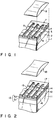
- a detailed structure of a thermal head of this type will be described below with reference to Fig. 1.
- reference numeral 1 denotes a metal substrate consisting of, e.g., an Fe-Cr alloy; and 2, a layer consisting of a polyimide resin represented by (formula 1).
- the polyimide resin layer 2 is obtained by coating and baking polyamic acid on the metal substrate 1.
- Polyamic acid is synthesized by substituting 0.05 to 10 mol% of p-phenylene diamine by bis-aminosiloxane upon ring-opening poly-addition reaction of an equimolar mixture of a biphenyl tetracarboxylic acid dihydride and p-phenylene diamine.
- Reference numeral 3 denotes an undercoating layer consisting of, e.g., SiO x , SiN, or SiC. The undercoating layer 3 is formed in order to protect the polyimide resin layer against chemical dry etching or ashing, facilitate control of a resistance upon formation of a heat-generating resistive layer 4, and improve a wire bonding property.
- Reference numeral 4 denotes a heat-generating resistor consisting of, e.g., Ta-SiO2 or Ti-SiO2.
- Discrete electrodes 6 and a common electrode 7 con sisting of, e.g., Al or Al-Si-Cu are formed on the heat-generating resistor 4 so as to form an opening to serve as a heat-generating portion 5.
- a protective layer 8 consisting of, e.g., Si-O-N, SiN, or SiC is formed so as to cover at least the heat-generating portion 5.
- the protective layer 8 is illustrated as a single layer in Fig. 1.
- a plurality of layers such as an oxidation-proofing layer and an abrasion-proofing layer may be formed independently from each other, or an oxidation-proofing/abrasion proofing layer and an adhesive layer may be formed.
- thermal head can sufficiently withstand an operation as a thermal head in terms of a heat-resistance and an adhesive force.
- a resistance abnormally changes to adversely affect a printing performance during the test.
- a singular point of a function at which the resistance abnormally changes as described above was carefully checked. As a result, it is found that hard foreign matters such as dust caught between the thermal head and heat-sensitive paper often causes a crack in the protective film, and the singular point of a function is produced when the crack reaches the heat-generating resistor.
- the surface protective layer Various materials, therefore, have been examined as the surface protective layer.
- Ta2O3 or SiO2 is unsatisfactory in hardness
- Si3N4, SiC, and Al2O3 is unsatisfactory in toughness
- materials of both these types produce cracks. That is, none of the material has sufficient properties to be used in the thermal head using a resin for the heat insulating layer.
- an example of a material not producing a crack is a SIALON film described in Japanese Patent Disclosure (KOKAI) Nos. 60-4077 and 62-3968. This SIALON film consists of Si, Al, O, and N as main components and has high hardness and toughness.
- a sputtering rate, however, upon formation of the SIALON film is low even in an Ar gas atmosphere.
- metal Al tends to precipitate to degrade an insulation property.
- this precipitation can be suppressed by adding 5% to 10% of O2 or N2 to the Ar gas, the sputtering rate is further decreased by this addition.
- a thermal head which comprises a high-resistance substrate, a heat-generating resistive layer formed on the high-resistance substrate, an electrode layer formed on the high-resistance substrate so as to be electrically connected to the heat-generating resistive layer, and a protective layer formed to cover at least a heat-generating portion of the heat-generating resistive layer.
- This protective layer consists of a compound containing Si, O, N, and a metal M which is at least one metal selected from the group consisting of Zr, Mg, and Y. Since the protective layer has high hardness and toughness, even if a local concentrated load acts on the protective layer during operation of the thermal head, the protective layer does not plastically deform much nor crack.
- this protective layer By using this protective layer, therefore, even if a heat insulating layer consisting of a soft material having high deformability such as a heat-resistant resin is included as an interlayer between the high-resistance substrate and the heat-generating resistive layer, since the protective layer has sufficient hardness for resisting deformation caused when a hard foreign matter is caught in and toughness which prevents a crack from being easily formed upon deformation to a certain extent, deformation, a crack, and the like caused by a local stress of the thermal head can be prevented. When this thermal head is used, reliability can be improved without degrading a printing performance. In addition, this protective layer can be formed at a higher sputtering rate than that of a conventional SIALON film and the like and is superior in a mass-production property.
- an Fe-Cr alloy for example, is used as a metal substrate 11.
- alloys containing, e.g., Al and Si in addition to Fe-Cr, and ceramics such as Al2O3 can also be used.
- a heat insulating layer 12 consisting of an aromatic polyimide resin represented by formula 1 below and having a thickness of about 5 to 50 »m, and preferably, 10 to 30 »m is formed as a heat insulating layer on the metal substrate 11. This polyimide resin is formed by coating and baking a polyamic acid varnish on the substrate 11.
- the polyamic acid varnish is prepared by substituting 5 mol% of p-phenylene diamine by bis-aminosiloxane to synthesize polyamic acid upon-ring opening poly-addition reaction of an equimolar mixture of, e.g., a biphenyl tetracarboxylic acid dihydride and p-phenylene diamine, and dissolving the obtained polyamic acid in an organic solvent.
- a polyamide resin, a polyamidoimide resin, a silicone resin, and the like can be used as the heat insulating layer 12.
- glazed glass can be used in place of the heat-resistant resin as a heat insulating layer 12, the substrate 11 and the heat insulating layer 12 are preferably a combination of a metal and a heat-resistant resin layer.
- the undercoating layer 13 is preferably constituted by at least one material selected from the group consisting of SiO x , SiON, SiN, SiC, and I-carbon.
- a heat-generating resistor 14 consisting of, e.g., Ta-SiO2 is formed on the undercoating layer 13, and discrete electrodes 16 and a common electrode 17 consisting of, e.g., Al are formed on the element 14.
- Heat-generating portions 15 are that parts of the heat-generating resistor 14 which are located between both the electrodes.
- a protective layer 18 consisting of a compound containing, e.g., Si, Zr, Y, N, and O is formed to cover the heat-generating portion 15, thereby completing the thermal head.
- the heat-generating resistor 14 of the heat-generating portion 15 when a pulse voltage is applied between the discrete and common electrodes 16 and 17 at a predetermined time interval, the heat-generating resistor 14 of the heat-generating portion 15 generates heat, thereby performing printing/recording.
- the present invention improves the protective film 18 of the thermal head.
- the film 18 consists of a compound containing Si, O, N, and a metal M (which is at least one metal selected from the group consisting of Zr, Mg, and Y).
- the film 18 preferably consists of a compound containing Si, O, N, Zr, and Y.
- an amount of Zr is preferably 1.0 to 40 mol% calculated in terms ot ZrO2. If the amount is less than 1.0 mol%, no sufficient hardness nor toughness can be obtained. If the amount exceeds 40 mol%, a large amount of a metal component is contained to degrade an insulation property of the protective layer.
- An amount of Y is preferably 0.1 to 10 mol% calculated in terms of Y2O3. If the amount is less than 0.1 mol%, no sufficient hardness nor toughness can be obtained. If the amount exceeds 10 mol%, a large amount of a metal component is contained to degrade the insulation property of the protective layer.
- An amount of Mg is preferably 0.1 to 10 mol% calculated in terms of MgO. If the amount is less than 0.1 mol%, no sufficient hardness nor toughness can be obtained. If the amount exceeds 10 mol%, a large amount of a metal component is contained to degrade the insulation property of the protective layer.
- the protective film 18 according to the present invention has higher hardness and toughness than those of a conventional protective film.
- a conventional SIALON film Al in the SIALON film properly disperses in the film as a metal component, thereby increasing the toughness.
- the hardness is increased since Zr and Y atoms bonded to N and O atoms are many as compared with Al atoms in SIALON, while a reduction in insulation property of the protective layer is small.
- a sputtering rate of the protective film according to the present invention is higher than that of the SIALON film and therefore is superior in a mass-production property.
- the thermal head of the present invention shown in Fig. 2 is manufactured, e.g., as follows.
- a metal substrate 11 consisting of an Fe alloy containing 18 wt% of Cr and having a thickness of about 0.5 mm is subjected to leveling, and cut into a predetermined size, and burr is removed therefrom. Thereafter, the metal substrate 11 is degreased/washed in an organic solvent, and dipped in diluted sulphuric acid maintained at 50°C to 70°C to remove an oxide layer formed on the surface and to perform an activation treatment to microscopically roughen the surface.
- the metal substrate 11 is washed with pure water and dried, and the above-described polyamic acid is adjusted to have a predetermined viscosity by using a solvent, e.g., N-methyl-2-pyrrolidone and coated on the metal substrate 11 to have a predetermined film thickness by using a roll coater, a spin coater, or the like.
- the resultant structure is heated in turn at 50°C for one hour, at 80°C for 30 minutes, at 120°C for 30 minutes, at 250°C for one hour, and at 450°C for one hour by using a sintering furnace to remove a solvent component and to accelerate a dehydrating cyclizing reaction so as to perform film formation, thereby forming a heat insulating layer 12.
- an undercoating layer 13 constituted by an SiN layer 31 and an SiC layer 32 is continuously formed on the heat insulating layer 12 at a substrate temperature of 150°C to 300°C by the plasma CVD method. That is, SiH4 gas and N2 gas are introduced to form the SiN layer 31, and then SiH4 gas and CH4 gas are introduced to form the SiC layer 32. Thereafter, a heat-generating resistor 14 consisting of Ta-SiO2, and discrete electrodes 16 and a common on electrode 17 consisting of Al are formed. Note that an opening serving to form a heat-generating portion 15 is obtained by forming an Al layer into a predetermined pattern by wet or dry etching after masking.
- Targets having compositions as listed in Table 1 below were used to perform sputtering in an Ar gas atmosphere in which a background pressure was 1 x 10 ⁇ 6 Torr and a pressure after Ar was introduced was 1 x 10 ⁇ 3 Torr, at a substrate temperature of 150°C to 200°C for a predetermined time, thereby forming protective films each having a film thickness of 3 »m.
- Each protective film was subjected to hardness estimation using a micro knoop hardness tester for thin films and fracture strength measurement using a scratch tester having a sensor for sensing acoustic emission generated upon film breaking.
- thermal heads having each protective film were assembled in facsimiles and operated, thereby performing a 10-km running test at a platen pressure of 160 g/cm and an application energy of 0.23 mJ/dot with a pulse width of 2.2 ms.
- the results are summarized in Table 1.
- Each layer thickness was 3 »m except for SiO2 (2 »m) + Ta2O5 (3 »m) in comparative examples.
- the protective layer according to the present invention has high hardness and toughness, can prevent a crack which tends to be produced when a resin is used as a heat insulating layer, can be produced at a high sputtering rate, and is superior in a mass-production property.
- a metal substrate is used as a support.
- the present invention is not limited to the above embodiment.
- a ceramic substrate or the like can be used.
Landscapes
- Electronic Switches (AREA)
- Non-Adjustable Resistors (AREA)
Claims (9)
- Thermokopf, umfassend ein Substrat (11) hohen Widerstands, eine auf dem Substrat (11) hohen Widerstands gebildete wärmeerzeugende Widerstandsschicht (14) mit einem wärmeerzeugenden Teil (15), auf dem Substrat (11) hohen Widerstands zum elektrischen Anschluß an die wärmeerzeugende Widerstandselementschicht (14) vorgesehene Elektrodenschichten (16, 17) und eine Schutzschicht (18) zum Bedecken zumindest des wärmeerzeugenden Teils (15) der wärmeerzeugenden Widerstandsschicht (14), wobei die Schutzschicht (18) eine Verbindung mit Si, O, N und einem Metall M umfaßt, dadurch gekennzeichnet, daß das Metall M aus mindestens einem solchen aus der Gruppe Zr, Mg und Y besteht.
- Thermokopf nach Anspruch 1, dadurch gekennzeichnet, daß es sich bei dem Metall M zumindest um ein solches aus der Gruppe Y und Zr handelt.
- Thermokopf nach Anspruch 1, dadurch gekennzeichnet, daß die Schutzschicht (18) eine Verbindung mit Si, O, N und Zr umfaßt, wobei der Zr-Gehalt der Verbindung, berechnet als ZrO₂, 1,0 bis 40 Mol% beträgt.
- Thermokopf nach Anspruch 1, dadurch gekennzeichnet, daß die Schutzschicht (18) eine Verbindung mit Si, O, N und Y umfaßt, wobei der Y-Gehalt der Verbindung, berechnet als Y₂O₃, 0,1 bis 10 Mol% beträgt.
- Thermokopf nach Anspruch 1, dadurch gekennzeichnet, daß das Substrat (11) hohen Widerstands eine Komponente, ausgewählt aus der Gruppe ein Metall, eine Legierung und einen Keramikwerkstoff, umfaßt.
- Thermokopf nach Anspruch 1, dadurch gekennzeichnet, daß die Wärmeisolierschicht (12) aus einem wärmebeständigen Harz zwischen dem Substrat hohen Widerstands und der wärmeerzeugenden Widerstandsschicht (14) vorgesehen ist.
- Thermokopf nach Anspruch 6, dadurch gekennzeichnet, daß das Substrat (11) hohen Widerstands ein Metall umfaßt.
- Thermokopf nach Anspruch 6, dadurch gekennzeichnet, daß das Substrat (11) hohen Widerstands eine Legierung umfaßt.
- Thermokopf nach Anspruch 6, dadurch gekennzeichnet, daß das Substrat (11) hohen Widerstands einen Keramikwerkstoff umfaßt.
Applications Claiming Priority (2)
| Application Number | Priority Date | Filing Date | Title |
|---|---|---|---|
| JP272943/88 | 1988-10-31 | ||
| JP63272943A JPH0626914B2 (ja) | 1988-10-31 | 1988-10-31 | サーマルヘッド |
Publications (2)
| Publication Number | Publication Date |
|---|---|
| EP0367122A1 EP0367122A1 (de) | 1990-05-09 |
| EP0367122B1 true EP0367122B1 (de) | 1994-07-13 |
Family
ID=17520931
Family Applications (1)
| Application Number | Title | Priority Date | Filing Date |
|---|---|---|---|
| EP89119935A Expired - Lifetime EP0367122B1 (de) | 1988-10-31 | 1989-10-26 | Wärmekopf |
Country Status (5)
| Country | Link |
|---|---|
| US (1) | US4985712A (de) |
| EP (1) | EP0367122B1 (de) |
| JP (1) | JPH0626914B2 (de) |
| KR (1) | KR920010608B1 (de) |
| DE (1) | DE68916748T2 (de) |
Families Citing this family (2)
| Publication number | Priority date | Publication date | Assignee | Title |
|---|---|---|---|---|
| JP3965508B2 (ja) * | 1996-02-08 | 2007-08-29 | 株式会社東芝 | サーマルプリントヘッド、サーマルプリントヘッドの製造方法、記録装置、焼結体およびターゲット |
| EP1226951A3 (de) * | 2001-01-29 | 2003-03-12 | Alps Electric Co., Ltd. | Energiesparthermokopf |
Family Cites Families (11)
| Publication number | Priority date | Publication date | Assignee | Title |
|---|---|---|---|---|
| JPS52100245A (en) * | 1976-02-19 | 1977-08-23 | Oki Electric Ind Co Ltd | Thermal head of high heat efficiency |
| JPS5582677A (en) * | 1978-12-18 | 1980-06-21 | Toshiba Corp | Thermal head |
| JPS609770A (ja) * | 1983-06-29 | 1985-01-18 | Kyocera Corp | サ−マルヘツド |
| JPS6135973A (ja) * | 1984-07-30 | 1986-02-20 | Hitachi Ltd | 感熱ヘツド |
| JPS623968A (ja) * | 1985-06-29 | 1987-01-09 | Noritake Co Ltd | 耐摩耗性薄膜サ−マルヘツド |
| GB2179007B (en) * | 1985-08-12 | 1990-09-12 | Mitsubishi Electric Corp | Thermal head for printer |
| JPS6290260A (ja) * | 1985-10-16 | 1987-04-24 | Tdk Corp | サ−マルヘツド用耐摩耗性保護膜 |
| JPS62252101A (ja) * | 1986-04-25 | 1987-11-02 | ティーディーケイ株式会社 | 抵抗発熱体 |
| EP0251036B1 (de) * | 1986-06-25 | 1991-05-08 | Kabushiki Kaisha Toshiba | Wärmekopf |
| JPS6374963A (ja) * | 1986-09-16 | 1988-04-05 | 株式会社豊田中央研究所 | 耐摩耗材用窒化けい素質焼結体 |
| JPS62275067A (ja) * | 1987-05-16 | 1987-11-30 | 日本碍子株式会社 | 窒化珪素焼結体の製造法 |
-
1988
- 1988-10-31 JP JP63272943A patent/JPH0626914B2/ja not_active Expired - Lifetime
-
1989
- 1989-10-26 EP EP89119935A patent/EP0367122B1/de not_active Expired - Lifetime
- 1989-10-26 DE DE68916748T patent/DE68916748T2/de not_active Expired - Lifetime
- 1989-10-26 US US07/426,865 patent/US4985712A/en not_active Expired - Lifetime
- 1989-10-31 KR KR1019890015675A patent/KR920010608B1/ko not_active Expired
Also Published As
| Publication number | Publication date |
|---|---|
| US4985712A (en) | 1991-01-15 |
| JPH0626914B2 (ja) | 1994-04-13 |
| KR920010608B1 (ko) | 1992-12-12 |
| DE68916748T2 (de) | 1994-12-22 |
| JPH02120057A (ja) | 1990-05-08 |
| DE68916748D1 (de) | 1994-08-18 |
| KR900006133A (ko) | 1990-05-07 |
| EP0367122A1 (de) | 1990-05-09 |
Similar Documents
| Publication | Publication Date | Title |
|---|---|---|
| US5831512A (en) | Resistance thermometer | |
| KR930004777B1 (ko) | 내열성 절연피복재 및 이것을 이용한 써말 헤드 | |
| EP0367122B1 (de) | Wärmekopf | |
| JP2597564B2 (ja) | サーマルヘツド | |
| JP2928525B2 (ja) | 保護膜形成用スパッタリングターゲット | |
| JPH01202465A (ja) | 保護被覆材およびそれを利用したサーマルヘッド | |
| JP2549136B2 (ja) | サーマルヘッド | |
| JP4925535B2 (ja) | サーマルヘッド | |
| KR920005317B1 (ko) | 내열성 절연기판, 서멀헤드 및 감열 기록 장치 | |
| JP3451026B2 (ja) | サーマルヘッド | |
| JP3323870B2 (ja) | サーマルプリンタヘッド | |
| JPH06256939A (ja) | スパッタリングターゲットおよびそれを用いて形成した高硬度被膜 | |
| JPH048554A (ja) | 耐熱性絶縁基板及びサーマルヘッド | |
| JP2568191Y2 (ja) | サーマルヘッド | |
| JP2003103820A (ja) | サーマルヘッド | |
| JPH0278573A (ja) | 耐熱性絶縁基板およびサーマルヘッド | |
| JPH01154770A (ja) | サーマルヘッド | |
| JP4925536B2 (ja) | サーマルヘッド | |
| JPH0278576A (ja) | 耐熱性絶縁基板およびサーマルヘッド | |
| KR920002533B1 (ko) | 서어멀 헤드(thermal head) | |
| JPH03293164A (ja) | サーマルヘッド | |
| JPH07108695A (ja) | 耐摩耗性被膜およびそれを用いたサーマルヘッド | |
| JPH0278575A (ja) | 耐熱性絶縁基板およびサーマルヘッド | |
| JPS6156111B2 (de) | ||
| JPH05338234A (ja) | サーマルヘッド |
Legal Events
| Date | Code | Title | Description |
|---|---|---|---|
| PUAI | Public reference made under article 153(3) epc to a published international application that has entered the european phase |
Free format text: ORIGINAL CODE: 0009012 |
|
| 17P | Request for examination filed |
Effective date: 19891123 |
|
| AK | Designated contracting states |
Kind code of ref document: A1 Designated state(s): DE FR GB |
|
| 17Q | First examination report despatched |
Effective date: 19930517 |
|
| GRAA | (expected) grant |
Free format text: ORIGINAL CODE: 0009210 |
|
| AK | Designated contracting states |
Kind code of ref document: B1 Designated state(s): DE FR GB |
|
| REF | Corresponds to: |
Ref document number: 68916748 Country of ref document: DE Date of ref document: 19940818 |
|
| ET | Fr: translation filed | ||
| PLBE | No opposition filed within time limit |
Free format text: ORIGINAL CODE: 0009261 |
|
| STAA | Information on the status of an ep patent application or granted ep patent |
Free format text: STATUS: NO OPPOSITION FILED WITHIN TIME LIMIT |
|
| 26N | No opposition filed | ||
| REG | Reference to a national code |
Ref country code: GB Ref legal event code: 746 Effective date: 19980909 |
|
| REG | Reference to a national code |
Ref country code: FR Ref legal event code: D6 |
|
| REG | Reference to a national code |
Ref country code: GB Ref legal event code: IF02 |
|
| PGFP | Annual fee paid to national office [announced via postgrant information from national office to epo] |
Ref country code: DE Payment date: 20081027 Year of fee payment: 20 |
|
| PGFP | Annual fee paid to national office [announced via postgrant information from national office to epo] |
Ref country code: FR Payment date: 20081014 Year of fee payment: 20 |
|
| PGFP | Annual fee paid to national office [announced via postgrant information from national office to epo] |
Ref country code: GB Payment date: 20081022 Year of fee payment: 20 |
|
| REG | Reference to a national code |
Ref country code: GB Ref legal event code: PE20 Expiry date: 20091025 |
|
| PG25 | Lapsed in a contracting state [announced via postgrant information from national office to epo] |
Ref country code: GB Free format text: LAPSE BECAUSE OF EXPIRATION OF PROTECTION Effective date: 20091025 |