EP0367496A2 - Vorrichtung und Verfahren zur Lithographie mittels eines Strahls geladener Teilchen - Google Patents
Vorrichtung und Verfahren zur Lithographie mittels eines Strahls geladener Teilchen Download PDFInfo
- Publication number
- EP0367496A2 EP0367496A2 EP89311047A EP89311047A EP0367496A2 EP 0367496 A2 EP0367496 A2 EP 0367496A2 EP 89311047 A EP89311047 A EP 89311047A EP 89311047 A EP89311047 A EP 89311047A EP 0367496 A2 EP0367496 A2 EP 0367496A2
- Authority
- EP
- European Patent Office
- Prior art keywords
- charged particle
- particle beam
- deflector
- mask
- optical axis
- Prior art date
- Legal status (The legal status is an assumption and is not a legal conclusion. Google has not performed a legal analysis and makes no representation as to the accuracy of the status listed.)
- Granted
Links
Images





Classifications
-
- H—ELECTRICITY
- H01—ELECTRIC ELEMENTS
- H01J—ELECTRIC DISCHARGE TUBES OR DISCHARGE LAMPS
- H01J37/00—Discharge tubes with provision for introducing objects or material to be exposed to the discharge, e.g. for the purpose of examination or processing thereof
- H01J37/30—Electron-beam or ion-beam tubes for localised treatment of objects
- H01J37/317—Electron-beam or ion-beam tubes for localised treatment of objects for changing properties of the objects or for applying thin layers thereon, e.g. for ion implantation
- H01J37/3174—Particle-beam lithography, e.g. electron beam lithography
- H01J37/3175—Projection methods, i.e. transfer substantially complete pattern to substrate
-
- B—PERFORMING OPERATIONS; TRANSPORTING
- B82—NANOTECHNOLOGY
- B82Y—SPECIFIC USES OR APPLICATIONS OF NANOSTRUCTURES; MEASUREMENT OR ANALYSIS OF NANOSTRUCTURES; MANUFACTURE OR TREATMENT OF NANOSTRUCTURES
- B82Y10/00—Nanotechnology for information processing, storage or transmission, e.g. quantum computing or single electron logic
-
- B—PERFORMING OPERATIONS; TRANSPORTING
- B82—NANOTECHNOLOGY
- B82Y—SPECIFIC USES OR APPLICATIONS OF NANOSTRUCTURES; MEASUREMENT OR ANALYSIS OF NANOSTRUCTURES; MANUFACTURE OR TREATMENT OF NANOSTRUCTURES
- B82Y40/00—Manufacture or treatment of nanostructures
-
- H—ELECTRICITY
- H01—ELECTRIC ELEMENTS
- H01J—ELECTRIC DISCHARGE TUBES OR DISCHARGE LAMPS
- H01J37/00—Discharge tubes with provision for introducing objects or material to be exposed to the discharge, e.g. for the purpose of examination or processing thereof
- H01J37/30—Electron-beam or ion-beam tubes for localised treatment of objects
- H01J37/317—Electron-beam or ion-beam tubes for localised treatment of objects for changing properties of the objects or for applying thin layers thereon, e.g. for ion implantation
- H01J37/3174—Particle-beam lithography, e.g. electron beam lithography
-
- H—ELECTRICITY
- H01—ELECTRIC ELEMENTS
- H01J—ELECTRIC DISCHARGE TUBES OR DISCHARGE LAMPS
- H01J2237/00—Discharge tubes exposing object to beam, e.g. for analysis treatment, etching, imaging
- H01J2237/15—Means for deflecting or directing discharge
-
- H—ELECTRICITY
- H01—ELECTRIC ELEMENTS
- H01J—ELECTRIC DISCHARGE TUBES OR DISCHARGE LAMPS
- H01J2237/00—Discharge tubes exposing object to beam, e.g. for analysis treatment, etching, imaging
- H01J2237/30—Electron or ion beam tubes for processing objects
- H01J2237/304—Controlling tubes
- H01J2237/30405—Details
- H01J2237/30411—Details using digital signal processors [DSP]
-
- H—ELECTRICITY
- H01—ELECTRIC ELEMENTS
- H01J—ELECTRIC DISCHARGE TUBES OR DISCHARGE LAMPS
- H01J2237/00—Discharge tubes exposing object to beam, e.g. for analysis treatment, etching, imaging
- H01J2237/30—Electron or ion beam tubes for processing objects
- H01J2237/317—Processing objects on a microscale
- H01J2237/3175—Lithography
- H01J2237/31761—Patterning strategy
- H01J2237/31762—Computer and memory organisation
-
- H—ELECTRICITY
- H01—ELECTRIC ELEMENTS
- H01J—ELECTRIC DISCHARGE TUBES OR DISCHARGE LAMPS
- H01J2237/00—Discharge tubes exposing object to beam, e.g. for analysis treatment, etching, imaging
- H01J2237/30—Electron or ion beam tubes for processing objects
- H01J2237/317—Processing objects on a microscale
- H01J2237/3175—Lithography
- H01J2237/31761—Patterning strategy
- H01J2237/31767—Step and repeat
-
- H—ELECTRICITY
- H01—ELECTRIC ELEMENTS
- H01J—ELECTRIC DISCHARGE TUBES OR DISCHARGE LAMPS
- H01J2237/00—Discharge tubes exposing object to beam, e.g. for analysis treatment, etching, imaging
- H01J2237/30—Electron or ion beam tubes for processing objects
- H01J2237/317—Processing objects on a microscale
- H01J2237/3175—Lithography
- H01J2237/31776—Shaped beam
Definitions
- the present invention generally relates to charged particle beam lithography and more particularly to a charged particle beam lithography system suitable for writing a semiconductor pattern on a semiconductor wafer and a method of writing such a pattern at a high speed.
- an extremely fine patterning according to the micron- or submicron-rule is possible by using a focused electron beam having an extremely small beam spot which may have a diameter of one micron or less.
- a so-called Gaussian beam having a circular beam spot with the Gaussian distribution for the electron intensity in the beam or a so-called shaped beam having a shaped beam cross section, which may be rectangular or triangular for example is used while moving a stage supporting a wafer continuously or stepwise.
- there is a limitation in the speed of patterning because of the essential nature of the electron beam lithography in which the pattern is written on the wafer by the electron beam in "one stroke".
- FIG.1 a system shown in FIG.1 is conventionally used in which an electron beam produced by an electron gun 1 is deflected by an electrostatic deflector 4 after passing through a shaping aperture 2 and an electromagnetic lens 3 such that the electron beam selectively falls on a designed pattern 6a provided on a stencil mask 5 in a form of aperture having a predetermined shape corresponding to the elementary pattern of the semiconductor device to be patterned. After passing through the mask 5, the electron beam now having a shape corresponding to the selected pattern 6a is focused on a wafer 7 by electron lenses 8 and 9.
- a rectangular or triangular aperture 6b and the cross section of the electron beam can be changed as desired by directing the electron beam to hit at least a part of the aperture 6b by controlling the electrostatic deflector 4.
- the deflector 4 By controlling the deflector 4 such that only a small part of the electron beam is passed through the aperture 6b, the size of the electron beam is reduced.
- the deflector 4 is controlled such that a large part of the electron beam is passed through the aperture 6b, the size of the electron beam is increased.
- FIG.2(A) shows a typical prior art mask 5 in more detail.
- the mask 5 generally comprises a silicon base body 5a on which a plurality of regions 6 are defined, wherein the predetermined patterns such as patterns 6a ⁇ 1 - 6a ⁇ 3 are formed in the region 6 in a form of the aperture as is clearly seen from the cross sectional view of FIG.2(B).
- the regions 6 are defined within an area 5b of the mask which can be addressed by the deflection of the electron beam B .
- the beam B having a desired cross section is moved over the wafer 7 by a deflection system (not shown) provided above the wafer 7 and a semiconductor pattern 7a comprising a repetition of patterns such as the pattern 6a ⁇ 3 and the like is written as a result of the movement of the beam B relative to the wafer 7 as shown in FIG.2(C).
- a marginal area written on the wafer 7 is represented as an area 7b.
- Such electron beam lithography using the mask is effective in patterning a semiconductor device particularly when the device comprises a repetition of a limited number of fundamental or elementary patterns such as dynamic random access memory (DRAM).
- DRAM dynamic random access memory
- the electrostatic deflector 4 is used to deflect the electron beam.
- the electrostatic deflector has a response time of about 0.1 - 1 ⁇ sec, the system can change the size and shape of the spot of the electron beam quickly between one shot and a next shot.
- the electrostatic deflector cannot produce a large beam deflection because of the practical limitation in the voltage applicable across a pair of electrodes forming the deflector.
- an excessive voltage is applied to the electrostatic deflector, there is a substantial risk that an electrical discharge is established between the electrodes and the control of the electron beam is lost.
- the deflection angle which can be obtained by the electrostatic deflector is limited and associated therewith, there is a problem in that the number of patterns which can be selected on the mask is limited.
- the prior art system of FIG.1 has a problem in that the electron lens 8 has a spherical abberation and an image formed on the wafer 7 in correspondence to the spot of the electron beam passed through the designed pattern tends to be blurred when the selected pattern is located at a marginal area far from the optical axis of the electron lens 8.
- the electron beam incident to the lens 8 which may comprise a first lens 8a and a second lens 8b as shown in the drawing, obliquely along a first path A (referred to as a beam A ) is spread relative to the electron beam incident perpendicularly to the lens 8 along a second path B passing straight through the center of the lens (referred to as a beam B ).
- Another and more specific object of the present invention is to provide a charged particle beam lithography system wherein a large variety of patterns are provided on a mask and a desired pattern is selectively used by deflecting a charged particle beam for a large deflection angle.
- Another object of the present invention is to provide a charged particle beam lithography system, wherein a variable shaping of the beam can be performed instantaneously between one shot and a next shot.
- Another object of the present invention is to provide a charged particle beam lithography system wherein formation of blur in a focused pattern caused by the spherical abberation of an electromagnetic lens is eliminated.
- Another object of the present invention is to provide a charged particle beam lithography system wherein the unwanted demagnification of a focused pattern on a semiconductor wafer is eliminated.
- Another object of the present invention is to provide a charged particle beam lithography system wherein a large deflection of a charged particle beam for addressing various patterns on a mask is made by an electromagnetic deflector while a small deflection for variable shaping of the beam is made by an electrostatic deflector.
- Another object of the present invention is to provide a charged particle beam lithography system for exposing an semiconductor wafer by a charged particle beam passed selectively through a plurality of apertures provided on a mask, comprising electrostatic deflection means and at least one electromagnetic deflection means for shaping the charged particle beam, wherein said electromagnetic deflection means deflects the charged particle beam such that the beam is passed through one of the apertures for providing a predetermined shape to the cross section of the charged particle beam and said electrostatic deflection means deflects the charged particle beam such that the beam is passed through a particular aperture on the mask for providing a variable shaped cross section to the charged particle beam.
- a number of predetermined patterns can be selected by deflecting the charged particle beam for a large angle by using the electromagnetic deflection means and the efficiency of the patterning process is improved. Further, when performing the exposure using the variable shaped beam, the shape of the charged particle beam can be changed instantaneously by using the electrostatic deflector and the efficiency of the patterning is improved also in this case.
- Another object of the present invention is to provide a charged particle beam lithography system for exposing an semiconductor wafer by a charged particle beam passed selectively through a plurality of apertures provided on a mask which in turn is provided inside an electromagnetic lens system, comprising first deflector means provided so as to deflect the charged particle beam proceeding along an optical axis away from the optical axis, second deflector means provided so as to deflect the charged particle beam deflected by the first deflector means such that the beam passes through the selected aperture in a direction substantially perpendicular to the mask, third deflector means provided so as to deflect the charged particle beam passed through the mask toward the optical axis and fourth deflector means provided so as to deflect the charged particle beam deflected by the third deflector means such that the electron beam travels along the optical axis.
- the spherical abberation of the electron magnetic lens system is eliminated by displacing the charged particle beam away from the optical axis while maintaining a parallel relationship after the beam has entered into the lens system and by returning the beam to the optical axis before the charged particle beam is exited from the lens system. Further, the foregoing problem of unwanted demagnification of the image associated with the oblique incidence of the charged particle beam to the electromagnetic lens system is successfully eliminated as the charged particle beam is entered and exited in and from the electromagnetic lens system substantially in coincidence with the optical axis.
- Another object of the present invention is to provide a method of writing a semiconductor pattern on a semiconductor wafer by a charged particle beam passed selectively through a plurality of apertures provided on a mask which in turn is provided inside an electron lens system, comprising steps of deflecting the charged particle beam proceeding along an optical axis selectively to one of said plurality of apertures by energizing first deflection means, deflecting the charged particle beam deflected by the foregoing first deflector means by energizing second deflection means such that the beam passes through the selected aperture in a direction substantially perpendicular to the mask, deflecting the charged particle beam passed through the mask by energizing third deflection means toward the optical axis, and deflecting the charged particle beam deflected by the third deflector means by energizing fourth deflection means such that the beam is propagated along the optical axis, wherein said third and fourth deflection means are energized according to a linearly independent combination of a parameter ⁇
- the adjustment of the charged particle beam for the beam alignment is performed easily as the lateral offset and the angular offset of the charged particle beam can be performed independently. Note that when the parameters X and Y are changed independently, in other words when the third and fourth deflection means are energized independently, the lateral offset and the angular offset of the charged particle beam passing through the mask are changed simultaneously and the proper alignment of the beam becomes extremely difficult.
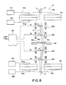
- FIG.4 shows an overall construction of the electron beam lithography system according to an embodiment of the present invention.
- an electron beam B produced by an electron gun 10 is, after adjustment by an electron beam adjusting system 11, shaped by passing through an aperture 12 and is focused at a crossover point 14x by an electron lens 14.
- the beam B is then entered to an electron lens 16 to be described and is focused at a second crossover point 16x.
- a mask 34 to be described is provided and the electron beam is shaped by passing through the aperture 12 and the mask 34.
- the electron beam is passed through demagnification lenses 20 and 22, and after passing through a round aperture 23, is converged by an objective lens system 24 such that a pattern carried on the mask 34 is formed on a semiconductor wafer 26 which in turn is held by a stage 28.
- the lens system 24 further includes an electromagnetic main deflector 24a and an electrostatic sub-deflector 24b for deflecting the electron beam on the wafer 26 so that the electron beam is moved over the surface of the wafer 26 to a desired position.
- the system of the present invention further comprises the foregoing stencil mask 34 carrying a plurality of apertures in a vicinity of or inside of the lens 16, and an electrostatic deflector 30 as well as an electromagnetic deflector 32 are further provided above the mask 34 for deflecting the electron beam B to a desired position on the mask 34. As illustrated in FIG.3, the deflector 30 and the deflector 32 are provided between the electron lens 14 and the electron lens 16.
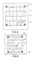
- FIG.5 shows the general construction of the mask 34.
- an area 71 which can be addressed by the electron beam B and a number of regions 72 are defined on the area 71 in correspondence to the region 6 of the prior art mask of FIG.2(A).
- the area 71 can be set substantially larger than the area 5b of the prior art mask 5 and a large variety of patterns such as a pattern 73a or 73b can be provided on the mask 34 without problem.
- the area 71 may have a size of 2 - 5 mm. In correspondence thereto, a range of deflection of about ⁇ 2.5 mm is needed for the electron beam. By using the electromagnetic deflector 32, such an area is easily covered.
- FIG.6 shows an actual construction of the mask 34.
- a number of the patterns 73 typically having a size of about 300 - 500 ⁇ m for each edge are arranged in the area 71 in a row and column formation except for a vicinity of a rectangular cutout 75 which is provided at a generally central part of the mask 34 close to the optical axis L for the variable shaping of the electron beam.
- the variable beam shaping is performed by shifting or offsetting the electron beam B relative to the cutout 75, the pattern 73 should not be provided in the vicinity of the cutout so as to avoid the leakage of the shifted electron beam B through a neighbouring pattern 73.
- a reference marker 79 at a suitable place on the mask 34 for the mask alignment.
- a large variety of patterns 73 can be provided on the mask 34.
- a shot for such a predetermined pattern would take a long time if the pattern is written one shot by one shot by a finely focused electron beam having a submicron size, for example.
- the use of electromagnetic deflector 32 which has a large response time which may be about 0.1 - 1 msec, does not cause inconvenience such as the decrease of efficiency in the patterning process.
- the variable shaped beam is used to write an irregular pattern by changing the size and shape of the beam in each shot.
- the present invention uses the electrostatic deflector 30 having a fast response time which may be about 0.1 - 1 ⁇ sec in combination with the cooperating cutout 75 provided in a vicinity of the optical axis.
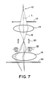
- FIG.7 shows the foregoing selection of the pattern 73 and the cutout 75 in the system of FIG.4.
- the electron beam B passing along an optical axis L is deflected by the electromagnetic deflector 32 as illustrated by a continuous line or a broken line.
- the electron beam is returned to the path extending along the optical axis L by the focusing action of the electron lens 16 which focuses the electron beam to the crossover point 16x located on the optical axis L .
- the electron beam B thus passed through the lens 16 is then passed through the mask 34 at a selected aperture on the mask as already described before passing through the crossover point 16x.
- the electron beam After passing through the crossover point 16x, the electron beam is demagnified by the lenses 22 and 24 and is focused on a surface of the wafer 26 by the objective lens 24. The electron beam is further moved over the surface of the wafer 26 by the main and sub-deflectors 24a and 24b.
- the electron beam lithography system of the present embodiment uses a control system which comprises a central processing unit (CPU) 40 and a large capacity storage means such as a magnetic disk storage 42 or a magnetic tape storage 44 in which a control program and the like for controlling the system are stored.
- CPU central processing unit
- a large capacity storage means such as a magnetic disk storage 42 or a magnetic tape storage 44 in which a control program and the like for controlling the system are stored.
- the CPU 40 sends a command to a pattern controller 50 via an interface 46 and a data memory 48, and the pattern controller 46 produces a control data specifying the deflection angle of the electron beam B in correspondence to the desired beam size and shape.
- This control data is then applied to the electrostatic deflector 30 in a form of a control voltage after digital-to-analog conversion in a D/A converter 51.
- the D/A converter 51 produces the control voltage corresponding to the desired angle of deflection and the electron beam B is moved over the mask 34 of FIG.6 such that only the desired portion of the electron beam is passed through the cutout 75.
- the response of the electrostatic deflector is instantaneous and a series of continuous shots can be achieved at a high speed while changing the size and shape of the beam in each shot.
- the CPU 40 sends a command to the pattern controller 50 via the interface 46 and the data memory 48 similarly to the foregoing case, whereby the pattern controller 50 produces a control data specifying a deflection angle of the electron beam for addressing the selected pattern 73 and the control data is converted into a control current to be supplied to the electromagnetic deflector 32 by a D/A converter 52. Responsive to the control current, the electron beam B is deflected by the foregoing specified angle and the electron beam moves over the mask 34 to the selected pattern 73. As a result of use of the electromagnetic deflector 32, the angle of deflection of the electron beam B can be set large and a large number of patterns 73 can be provided on the mask 34.
- the pattern controller further supplies a control data to a blanking controller 54 responsive to a command by the CPU 40 when interrupting the exposure. Responsive to the control data, the blanking controller 54 produces a blank control data and the blank control data is supplied to another electrostatic deflector 36 after a digital-to-analog conversion in a D/A converter 55. Responsive thereto, the electron beam is shifted from the optical path L passing through the pinhole 23 and the electron beam is disappeared from the surface of the wafer 26.
- the electron beam is moved over the surface of the wafer 26 responsive to the command signal from the CPU 40 which is supplied to a sequential controller 56 via the interface 46.
- the sequential controller 56 produces a data specifying the position of the electron beam on the wafer 26 and the data is supplied to a deflection controller 57.
- the deflection controller 57 in turn produces a first deflection control data representing the angle of deflection of the electron beam to be achieved by the main deflector 24a and a second deflection control data representing the angle of deflection of the beam to be achieved by the sub-deflector 24b.
- the first deflection control data is then converted to a deflection control current by a D/A converter 58 and is supplied to the main deflector 24a.
- the second deflection control data is converted to a deflection control voltage by a D/A converter 59 and is applied to the sub-deflector 24b.
- the sequential controller 56 supplies a stage control data specifying a desired position of the stage 28 to a stage controller 61 responsive to the command from the CPU 40 and the stage controller changes the position of the stage according to the stage control data supplied thereto. Further, the position of the stage 28 is monitored by a laser interferometer 59 and the deflection angle of the electron beam on the wafer 26 is adjusted according to the result of the positional measurement of the stage 28 by the laser interferometer 60.
- the electron lens 16 used in this embodiment comprises an upper lens 16a located at a side of the mask 34 closer to the electron gun 10 and a lower lens 16b located at the other side of the mask 34 closer to the stage 26.
- the electron lens 16 of this embodiment forms a lens system.
- the present embodiment uses four electromagnetic deflectors 32a - 32d provided between the electron lens 16a and the electron lens 16c in place of the electromagnetic deflector 32, in which two of them (32a and 32b) are disposed above the mask 34 and the remaining two of them (32c and 32d) are disposed below the mask.
- the electromagnetic deflectors 32a - 32d are energized by control currents S1 - S4 supplied from the pattern controller 50.
- the D/A converter 52 is omitted for the sake of simplicity.
- a current of about ⁇ 2 - 3 amperes is supplied as the control currents S1 - S4 while applying a voltage of about ⁇ 30 volts to the electrostatic deflector 30.
- the electromagnetic deflector 32a Responsive to the control current S1 produced by the pattern controller 50 under the control of the CPU 40, the electromagnetic deflector 32a produces a magnetic field + A as shown in the drawing.
- the electromagnetic deflector 32b located between the electromagnetic deflector 32a and the mask 34 produces a magnetic field - A having a same magnitude but an opposite direction as also illustrated in the drawing.
- the electromagnetic deflector 32c located below the mask 34 is supplied with the control current S3 from the pattern controller 50 and produces a magnetic filed - A which is identical to the magnetic field produced by the electromagnetic deflector 32b.
- the electromagnetic deflector 32d produces a magnetic field + A which is identical to the magnetic field produced by the electromagnetic deflector 32a.
- the electron beam B traveling along the optical axis L is passed through the upper electron lens 16a, the electron beam is deflected away from the optical axis L by the action of the magnetic field + A of the electromagnetic deflector 32a.
- the electron beam thus deflected is then deflected again by the magnetic field - A of the electromagnetic deflector 32b acting in the opposite direction with a same strength and the electron beam assumes a path extending parallel to the optical axis L but offset therefrom.
- the electron beam B passes through the mask 34 perpendicularly.
- the electron beam After passing through the mask 34, the electron beam is again deflected by the magnetic field - A produced by the electromagnetic deflector 32c toward the optical axis L by a same deflection angle as that when the beam is deflected by the electromagnetic deflector 32b.
- the electron beam B When returned on the optical axis L , the electron beam B is further deflected by the magnetic field + A produced by the electromagnetic deflector 32d by a deflection angle which is the same as that when the beam is deflected by the electromagnetic deflector 32a.
- the electron beam B is returned to the optical axis L and passes through the lower electron lens 16c along the optical axis L .
- the electron beam B enters to and exits from the lens system 16 substantially along the optical axis L even when the electron beam B is deflected for selectively addressing a desired pattern on the mask 34.
- the problem of spherical abberation is entirely eliminated. Further, the problem of unwanted demagnification of the image on the wafer 26 associated with the oblique incidence of the electron beam to the lens system 16 is entirely eliminated. Further, as a result of use of the electromagnetic deflectors, a large deflection angle is achieved and a wide variety of patterns on the mask 34 can be addressed by the electron beam B as desired similarly to the foregoing embodiment.
- control currents S2 - S4 are determined uniquely by the control current S1 in the controller 50 as the control currents S2 - S4 are in principle dependent on the control current S1.
- calibrating the actual deflection angle of the deflectors 32a - 32d in advance such a automatic determination of the control currents S2 - S4 by the control current S1 becomes possible. By doing so, the load of the controller 50 can be reduced and the efficiency of the patterning process is improved.
- the deflection angle is generally small.
- the construction of the deflector 30 for achieving the entering and exiting of the electron beam B in coincidence with the optical axis L is not absolutely necessary.
- a similar deflector arrangement for realizing this can be easily constructed from FIG.8 as shown in FIG.9.
- four electrostatic deflectors 30a - 30d are provided in place of the electrostatic deflector 30 of FIG.4 such that two of them (30a and 30b) are located above the mask 34 and two of them (30c and 30d) are located below the mask 34.
- Each of the electrostatic deflectors 30a - 30d is supplied with one of control voltages V1 - V4 from the pattern controller 50 under the control of the CPU 40 and deflects the electron beam B similarly to the case of FIG.8.
- the pattern controller 50 controls the voltages V1 - V4 such that an electric field having a same magnitude A but an opposite direction is established across a pair of electrodes forming the deflector.
- an electric field + A is formed by the electrostatic deflector 30a responsive to the control voltage V1
- an electric field - A is formed by the electrostatic deflector 30b responsive to the control voltage V2
- an electric field - A is formed by the electrostatic deflector 30c responsive to the control voltage V3
- an electric field + A is formed by the electrostatic deflector 30d responsive to the control voltage V4.
- Other operational principle is obvious from the foregoing description for the system of FIG.8 and further description of this system will be omitted.
- a voltage of about ⁇ 200 - 250 V is applied for a deflection angle of ⁇ 1 - 1.5 mm. According to this modification, a very quick deflection of the electron beam is possible.
- the angle of deflection achieved by this system is smaller than that obtained by the system of FIG.8, the system is effective when used in the case where a small deflection is needed with a very quick response.
- a doublet lens system is used for the electron lenses 16a and 16b in order to correct the rotation of the image.
- a rotation of the image is caused by the mask provided in the optical path of the electron beam.
- the rotation of the image has been corrected by rotating the mask.
- the rotation of the mask 43 in the system of the present invention is not preferable as such a rotation of the mask 34 causes a displacement of the patterns on the mask.
- the correction for the rotation of the image itself can be performed by a singlet electromagnetic lens. However, if such a singlet lens is used, the intensity of the magnetic field is also changed responsive to the rotation correction and the parallelism of the electron beam is lost or degraded.
- the electron lens 16a is formed as a doublet lens system comprising a first lens coil 16a1 driven by a first power source 161 and a second lens coil 16a2 driven by a second power source 162 as shown in FIG.8 so as to correct the rotation of the electron beam on the mask 34.
- the first coil 16a1 may be turned for five hundred times and the second coil 16a2 may be turned also for five hundred times and a current I is supplied to each of the coils with mutually opposing directions.
- the lower electron lens 16c is constructed as a doublet lens system comprising a first lens coil 16a3 and a second lens coil 16a4 driven by power sources 163 and 164 so as to correct the rotation of the image focused on the wafer 26.
- the correction of rotation of the beam by any lens coil provided below the lens 16c without using the doublet construction for the lens 16c is unrealistic as such a correction, performed each time the mask is replaced, inevitably invites change of strength of the magnetic field.
- the deflection for a small angle such as the case of variable shaping of the beam or small shift of the beam is made by the electrostatic deflector having a quick response while the deflection for a large angle is made by the electromagnetic deflector.
- the electron beam is incident somewhat obliquely to the mask 34 and as a result of the deflection by the electromagnetic deflectors 32c and 32d, the beam exited from the lower electron lens 16b is offset from the optical axis L .
- the electron beam B is focused on the wafer 26 at a position which is deviated from the desired position or is prevented from arriving at the wafer 26 by the round aperture 23.
- the present invention provides a method of adjusting the path of the electron beam B by once decomposing the offset of the electron beam into an angular offset component ⁇ representing a deviation of the beam direction from vertical and further into a lateral offset component ⁇ representing a lateral deviation of the beam from the properly aligned beam path, and further by changing these offset components ⁇ and ⁇ independently. Note that when the same adjustment is attempted by energizing the electromagnetic deflectors 32c and 32d independently, these offset components are changed simultaneously and the proper adjustment of the electron beam path becomes extremely difficult. This means that it takes a long time for achieving the beam alignment and the cost of the semiconductor device manufactured using the electron beam lithography technique is increased.
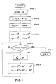
- FIG.11 shows a flowchart for the beam alignment process according to the present embodiment.
- the electron gun 10 is turned on in a step 1 and the electron beam B is formed.
- electrical energizations X1 - X4 which may be the control currents S1 - S4 to the electromagnetic deflector 32a - 32d are deenergized.
- the electron beam B is passed through the electromagnetic deflectors straight without deflection.
- the step 2 may be performed simultaneously or prior to the step 1.
- the beam adjusting system 11 shown in FIG.4 is adjusted in a step 3 until the electron beam B is passed through the pinhole 23.
- the electric energizations X1 - X4 are set respectively to + ⁇ s 1 , - ⁇ s 1 , - ⁇ s 1 and + ⁇ s 1 such that the electromagnetic deflectors 32a - 32d produce the magnetic fields + A, - A, - A and + A as already described.
- the electron beam is deflected as already described with reference to FIG.8. If the alignment is ideal, the electron beam passes through an ideal path shown in FIG.10 by a broken line and no further adjustment is necessary.
- a parameter ⁇ s 1 for the adjustment of the lateral offset ⁇ and a parameter ⁇ b for the adjustment of the angular offset ⁇ are changed in a step 7.
- the discrimination in the step 5 is performed again and the steps 5, 7 and 8 are repeated with a different combination of the electric energizations ⁇ s p and ⁇ b until the electron beam B is passed through the pinhole 23.
- FIG.12(A) shows the adjustment of the lateral offset ⁇ of the electron beam B responsive to the change of the electric energization ⁇ s p and FIG.12(B) shows the adjustment of the angular offset ⁇ of the electron beam B responsive to the change of the electric energization ⁇ b .
- the adjustment for the lateral offset component ⁇ in FIG.12(A) and the adjustment of the angular offset component ⁇ in FIG.12(B) can be performed independently and the process for alignment of the electron beam becomes significantly easier.
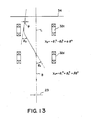
- FIG.13 shows a situation in which the beam alignment is achieved properly.
- the electric energization X3 is increased by - ⁇ s p + ⁇ . ⁇ b relative to the initial value of - ⁇ s 1 and the electric energization X4 by + ⁇ s p + ⁇ . ⁇ b .
- deflection angles ⁇ 3 and ⁇ 4 are changed and the electron beam B returns exactly on the optical axis L .
- the foregoing adjustment is not limited to the electromagnetic deflectors 32c and 32d but also applicable to the electromagnetic deflectors 32a and 32b.
- the adjustment of the beam path using the deflectors 32a and 32b is obvious from the foregoing description, the description for this case will be omitted.
- the charged particle beam is not limited to the electron beam but other charged particle beams such as proton beam or ionic beam may be used.
- the present invention is not limited to the system for writing a pattern on a semiconductor substrate but one may write a pattern on a reticle 26′ by placing it in the place of the semiconductor wafer 26 as shown in FIG.1.
Landscapes
- Engineering & Computer Science (AREA)
- Chemical & Material Sciences (AREA)
- Nanotechnology (AREA)
- Physics & Mathematics (AREA)
- Crystallography & Structural Chemistry (AREA)
- Analytical Chemistry (AREA)
- Mathematical Physics (AREA)
- Theoretical Computer Science (AREA)
- Condensed Matter Physics & Semiconductors (AREA)
- General Physics & Mathematics (AREA)
- Manufacturing & Machinery (AREA)
- Electron Beam Exposure (AREA)
Applications Claiming Priority (6)
| Application Number | Priority Date | Filing Date | Title |
|---|---|---|---|
| JP63275336A JPH02122518A (ja) | 1988-10-31 | 1988-10-31 | 半導体装置の製造方法 |
| JP275336/88 | 1988-10-31 | ||
| JP68308/89 | 1989-03-20 | ||
| JP1068308A JP2843594B2 (ja) | 1989-03-20 | 1989-03-20 | 荷電粒子ビーム露光装置及びその露光方法 |
| JP182151/89 | 1989-07-14 | ||
| JP1182151A JPH0346320A (ja) | 1989-07-14 | 1989-07-14 | 微細パターン露光方法 |
Publications (3)
| Publication Number | Publication Date |
|---|---|
| EP0367496A2 true EP0367496A2 (de) | 1990-05-09 |
| EP0367496A3 EP0367496A3 (en) | 1990-08-22 |
| EP0367496B1 EP0367496B1 (de) | 1994-12-28 |
Family
ID=27299698
Family Applications (1)
| Application Number | Title | Priority Date | Filing Date |
|---|---|---|---|
| EP89311047A Expired - Lifetime EP0367496B1 (de) | 1988-10-31 | 1989-10-26 | Vorrichtung und Verfahren zur Lithographie mittels eines Strahls geladener Teilchen |
Country Status (4)
| Country | Link |
|---|---|
| US (1) | US5051556A (de) |
| EP (1) | EP0367496B1 (de) |
| KR (1) | KR930002576B1 (de) |
| DE (1) | DE68920281T2 (de) |
Cited By (7)
| Publication number | Priority date | Publication date | Assignee | Title |
|---|---|---|---|---|
| EP0434990A3 (en) * | 1989-11-30 | 1991-09-11 | Fujitsu Limited | Charged-particle beam exposure method and apparatus |
| EP0494737A3 (en) * | 1991-01-11 | 1993-08-11 | Fujitsu Limited | Charged particle beam exposure device for improving the heating state of block mask |
| EP0603555A1 (de) * | 1992-12-22 | 1994-06-29 | Carl Zeiss | Verfahren zur Beleuchtung mit einem fokussierten Elektronenstrahl und zugehöriges elektronen-optisches Beleuchtungssystem |
| GB2301759A (en) * | 1995-06-02 | 1996-12-11 | Mitsubishi Electric Corp | Charged particle beam drawing data production apparatus |
| EP0769800A3 (de) * | 1995-10-20 | 1997-12-17 | AT&T Corp. | Vorrichtung zur Steuerung eines Ladungsträgerstrahls und lithographisches Verfahren unter Verwendung dieser Vorrichtung |
| WO1999053519A1 (en) * | 1998-04-10 | 1999-10-21 | Etec Systems, Inc. | Shaped shadow projection for an electron beam column |
| US6657211B2 (en) | 2000-07-14 | 2003-12-02 | Leo Elektronenmikroskopie | Process for electron beam lithography, and electron-optical lithography system |
Families Citing this family (25)
| Publication number | Priority date | Publication date | Assignee | Title |
|---|---|---|---|---|
| JPH04162710A (ja) * | 1990-10-26 | 1992-06-08 | Fujitsu Ltd | 電子ビーム露光装置 |
| US5391886A (en) * | 1991-08-09 | 1995-02-21 | Fujitsu Limited | Charged particle beam exposure system and method of exposing a pattern on an object by such a charged particle beam exposure system |
| US5349197A (en) * | 1991-09-30 | 1994-09-20 | Fujitsu Limited | Method for exposing a pattern on an object by a charged particle beam |
| JP2706192B2 (ja) * | 1991-11-06 | 1998-01-28 | 富士通株式会社 | 電子ビーム露光装置 |
| JP3212360B2 (ja) * | 1992-06-16 | 2001-09-25 | 株式会社日立製作所 | マスクの製造方法、および半導体集積回路装置の製造方法 |
| US5455427A (en) * | 1993-04-28 | 1995-10-03 | Lepton, Inc. | Lithographic electron-beam exposure apparatus and methods |
| US5650628A (en) * | 1994-12-15 | 1997-07-22 | International Business Machines Corporation | Simultaneous deflections in charged-particle beams |
| JPH10144583A (ja) * | 1996-11-07 | 1998-05-29 | Nikon Corp | 荷電粒子線投影方法および荷電粒子線投影装置 |
| JP4156700B2 (ja) * | 1998-03-16 | 2008-09-24 | 富士通株式会社 | 露光データ作成方法、露光データ作成装置、及び、記録媒体 |
| US6437352B1 (en) * | 1999-06-01 | 2002-08-20 | Nikon Corporation | Charged particle beam projection lithography with variable beam shaping |
| EP1210723B1 (de) | 2000-01-21 | 2009-03-18 | Fei Company | Fokussierte ionenstrahlen mit vorgegebener form und geringer dichte |
| US6727500B1 (en) * | 2000-02-25 | 2004-04-27 | Fei Company | System for imaging a cross-section of a substrate |
| US6977386B2 (en) * | 2001-01-19 | 2005-12-20 | Fei Company | Angular aperture shaped beam system and method |
| US7160475B2 (en) * | 2002-11-21 | 2007-01-09 | Fei Company | Fabrication of three dimensional structures |
| US7034297B2 (en) * | 2003-03-05 | 2006-04-25 | Applied Materials, Israel, Ltd. | Method and system for use in the monitoring of samples with a charged particle beam |
| JP3968338B2 (ja) * | 2003-10-08 | 2007-08-29 | 株式会社東芝 | 荷電ビーム露光装置 |
| JP2005276869A (ja) * | 2004-03-23 | 2005-10-06 | Jeol Ltd | 荷電粒子ビーム描画装置。 |
| KR100601978B1 (ko) * | 2004-12-20 | 2006-07-18 | 삼성전자주식회사 | 전자빔 리소그래피 시스템의 전자기 포커싱 방법 |
| JP4528308B2 (ja) * | 2004-12-28 | 2010-08-18 | パイオニア株式会社 | ビーム記録方法及び装置 |
| US7209055B1 (en) * | 2005-10-03 | 2007-04-24 | Applied Materials, Inc. | Electrostatic particle beam deflector |
| JP5007063B2 (ja) * | 2006-03-31 | 2012-08-22 | 株式会社ニューフレアテクノロジー | 荷電粒子ビーム装置、da変換装置の異常検出方法、荷電粒子ビーム描画方法及びマスク |
| US8900982B2 (en) * | 2009-04-08 | 2014-12-02 | Varian Semiconductor Equipment Associates, Inc. | Techniques for processing a substrate |
| WO2012012548A2 (en) * | 2010-07-20 | 2012-01-26 | The Research Foundation Of State University Of New York | Methods, devices, and systems for manipulating charged particle streams |
| WO2016182948A1 (en) * | 2015-05-08 | 2016-11-17 | Kla-Tencor Corporation | Method and system for aberration correction in electron beam system |
| DE102021122388A1 (de) * | 2021-08-30 | 2023-03-02 | Carl Zeiss Microscopy Gmbh | Teilchenstrahlsäule |
Family Cites Families (5)
| Publication number | Priority date | Publication date | Assignee | Title |
|---|---|---|---|---|
| US4213053A (en) * | 1978-11-13 | 1980-07-15 | International Business Machines Corporation | Electron beam system with character projection capability |
| JPS55146931A (en) * | 1979-05-04 | 1980-11-15 | Hitachi Ltd | Depicting method by electronic beam |
| FR2488043A1 (fr) * | 1980-07-30 | 1982-02-05 | Le N Proizv | Dispositif a optique electronique pour l'etude d'echantillons |
| JPS58218117A (ja) * | 1982-06-11 | 1983-12-19 | Fujitsu Ltd | 電子ビ−ム制御装置 |
| JPH0793253B2 (ja) * | 1986-10-31 | 1995-10-09 | 株式会社東芝 | 荷電ビ−ム露光装置 |
-
1989
- 1989-10-26 EP EP89311047A patent/EP0367496B1/de not_active Expired - Lifetime
- 1989-10-26 DE DE68920281T patent/DE68920281T2/de not_active Expired - Fee Related
- 1989-10-30 KR KR8915615A patent/KR930002576B1/ko not_active Expired - Fee Related
- 1989-10-31 US US07/429,500 patent/US5051556A/en not_active Expired - Lifetime
Cited By (12)
| Publication number | Priority date | Publication date | Assignee | Title |
|---|---|---|---|---|
| EP0434990A3 (en) * | 1989-11-30 | 1991-09-11 | Fujitsu Limited | Charged-particle beam exposure method and apparatus |
| US5130547A (en) * | 1989-11-30 | 1992-07-14 | Fujitsu Limited | Charged-particle beam exposure method and apparatus |
| EP0494737A3 (en) * | 1991-01-11 | 1993-08-11 | Fujitsu Limited | Charged particle beam exposure device for improving the heating state of block mask |
| EP0603555A1 (de) * | 1992-12-22 | 1994-06-29 | Carl Zeiss | Verfahren zur Beleuchtung mit einem fokussierten Elektronenstrahl und zugehöriges elektronen-optisches Beleuchtungssystem |
| US5483073A (en) * | 1992-12-22 | 1996-01-09 | Carl-Zeiss-Stiftung | Method of illuminating an object with a focused electron beam and an electron-optical illuminating system therefor |
| GB2301759A (en) * | 1995-06-02 | 1996-12-11 | Mitsubishi Electric Corp | Charged particle beam drawing data production apparatus |
| US5796408A (en) * | 1995-06-02 | 1998-08-18 | Mitsubishi Denki Kabushiki Kaisha | Charged particle beam drawing data production apparatus and charged particle beam drawing system |
| GB2301759B (en) * | 1995-06-02 | 1999-08-04 | Mitsubishi Electric Corp | Charged particle beam drawing system including charged particle beam drawing data production apparatus |
| EP0769800A3 (de) * | 1995-10-20 | 1997-12-17 | AT&T Corp. | Vorrichtung zur Steuerung eines Ladungsträgerstrahls und lithographisches Verfahren unter Verwendung dieser Vorrichtung |
| WO1999053519A1 (en) * | 1998-04-10 | 1999-10-21 | Etec Systems, Inc. | Shaped shadow projection for an electron beam column |
| US6657211B2 (en) | 2000-07-14 | 2003-12-02 | Leo Elektronenmikroskopie | Process for electron beam lithography, and electron-optical lithography system |
| EP1172837A3 (de) * | 2000-07-14 | 2006-07-05 | LEO Elektronenmikroskopie GmbH | Verfahren zur Elektronenstrahl-Lithographie und elektronen-optisches Lithographiesystem |
Also Published As
| Publication number | Publication date |
|---|---|
| US5051556A (en) | 1991-09-24 |
| KR900007052A (ko) | 1990-05-09 |
| EP0367496B1 (de) | 1994-12-28 |
| EP0367496A3 (en) | 1990-08-22 |
| DE68920281D1 (de) | 1995-02-09 |
| DE68920281T2 (de) | 1995-05-11 |
| KR930002576B1 (en) | 1993-04-03 |
Similar Documents
| Publication | Publication Date | Title |
|---|---|---|
| EP0367496B1 (de) | Vorrichtung und Verfahren zur Lithographie mittels eines Strahls geladener Teilchen | |
| US5173582A (en) | Charged particle beam lithography system and method | |
| US6472672B1 (en) | Electron beam exposure apparatus and its control method | |
| US6552353B1 (en) | Multi-electron beam exposure method and apparatus and device manufacturing method | |
| US6472674B1 (en) | Electron beam exposure system and method of manufacturing devices using the same | |
| JP3940824B2 (ja) | 荷電粒子線によるパターン転写方法および転写装置 | |
| US6835937B1 (en) | Correcting method for correcting exposure data used for a charged particle beam exposure system | |
| JP5475155B2 (ja) | 投影レンズ構成体 | |
| EP0051733A1 (de) | Elektronenstrahl-Projektionseinrichtung | |
| US6104035A (en) | Electron-beam exposure apparatus and method | |
| JPH09223475A (ja) | 電磁偏向器、及び該偏向器を用いた荷電粒子線転写装置 | |
| US11804360B2 (en) | Multi charged particle beam adjustment method, multi charged particle beam irradiation method, and multi charged particle beam irradiation apparatus | |
| JPH1064812A (ja) | 電子ビーム露光方法及びそれを用いたデバイス製造方法 | |
| US5635719A (en) | Variable curvilinear axis deflection means for particle optical lenses | |
| US6903352B2 (en) | Charged-particle beam exposure apparatus, charged-particle beam exposure method, control data determination method, and device manufacturing method using this method | |
| JP2000012438A (ja) | マルチ電子ビーム露光方法及び装置、ならびにデバイス製造方法 | |
| US5793048A (en) | Curvilinear variable axis lens correction with shifted dipoles | |
| EP0883891B1 (de) | Verfahren zum betreiben eines partikels optischen gerätes | |
| US5708274A (en) | Curvilinear variable axis lens correction with crossed coils | |
| US5631113A (en) | Electron-beam exposure system for reduced distortion of electron beam spot | |
| EP0088457B1 (de) | Strahlgerät mit geladenen Teilchen | |
| JP4018197B2 (ja) | 電子ビーム露光方法及び電子ビーム露光装置 | |
| JPH11195590A (ja) | マルチ電子ビーム露光方法及び装置、ならびにデバイス製造方法 | |
| US7173262B2 (en) | Charged particle beam exposure apparatus, charged particle beam exposure method and device manufacturing method | |
| EP0780879A2 (de) | Elektronenstrahl-Belichtungsgerät |
Legal Events
| Date | Code | Title | Description |
|---|---|---|---|
| PUAI | Public reference made under article 153(3) epc to a published international application that has entered the european phase |
Free format text: ORIGINAL CODE: 0009012 |
|
| AK | Designated contracting states |
Kind code of ref document: A2 Designated state(s): DE FR GB |
|
| PUAL | Search report despatched |
Free format text: ORIGINAL CODE: 0009013 |
|
| AK | Designated contracting states |
Kind code of ref document: A3 Designated state(s): DE FR GB |
|
| RHK1 | Main classification (correction) |
Ipc: H01J 37/30 |
|
| 17P | Request for examination filed |
Effective date: 19901126 |
|
| 17Q | First examination report despatched |
Effective date: 19920814 |
|
| RBV | Designated contracting states (corrected) |
Designated state(s): DE GB |
|
| GRAA | (expected) grant |
Free format text: ORIGINAL CODE: 0009210 |
|
| AK | Designated contracting states |
Kind code of ref document: B1 Designated state(s): DE GB |
|
| REF | Corresponds to: |
Ref document number: 68920281 Country of ref document: DE Date of ref document: 19950209 |
|
| PLBE | No opposition filed within time limit |
Free format text: ORIGINAL CODE: 0009261 |
|
| STAA | Information on the status of an ep patent application or granted ep patent |
Free format text: STATUS: NO OPPOSITION FILED WITHIN TIME LIMIT |
|
| 26N | No opposition filed | ||
| REG | Reference to a national code |
Ref country code: GB Ref legal event code: IF02 |
|
| PGFP | Annual fee paid to national office [announced via postgrant information from national office to epo] |
Ref country code: GB Payment date: 20041020 Year of fee payment: 16 |
|
| PGFP | Annual fee paid to national office [announced via postgrant information from national office to epo] |
Ref country code: DE Payment date: 20041021 Year of fee payment: 16 |
|
| PG25 | Lapsed in a contracting state [announced via postgrant information from national office to epo] |
Ref country code: GB Free format text: LAPSE BECAUSE OF NON-PAYMENT OF DUE FEES Effective date: 20051026 |
|
| PG25 | Lapsed in a contracting state [announced via postgrant information from national office to epo] |
Ref country code: DE Free format text: LAPSE BECAUSE OF NON-PAYMENT OF DUE FEES Effective date: 20060503 |
|
| GBPC | Gb: european patent ceased through non-payment of renewal fee |
Effective date: 20051026 |