EP0368442A2 - Optischer Informationsaufzeichnungsträger und Verfahren zu seiner Herstellung - Google Patents
Optischer Informationsaufzeichnungsträger und Verfahren zu seiner Herstellung Download PDFInfo
- Publication number
- EP0368442A2 EP0368442A2 EP89307379A EP89307379A EP0368442A2 EP 0368442 A2 EP0368442 A2 EP 0368442A2 EP 89307379 A EP89307379 A EP 89307379A EP 89307379 A EP89307379 A EP 89307379A EP 0368442 A2 EP0368442 A2 EP 0368442A2
- Authority
- EP
- European Patent Office
- Prior art keywords
- layer
- reflecting
- record carrier
- layers
- transparent
- Prior art date
- Legal status (The legal status is an assumption and is not a legal conclusion. Google has not performed a legal analysis and makes no representation as to the accuracy of the status listed.)
- Granted
Links
Images


Classifications
-
- G—PHYSICS
- G11—INFORMATION STORAGE
- G11B—INFORMATION STORAGE BASED ON RELATIVE MOVEMENT BETWEEN RECORD CARRIER AND TRANSDUCER
- G11B7/00—Recording or reproducing by optical means, e.g. recording using a thermal beam of optical radiation by modifying optical properties or the physical structure, reproducing using an optical beam at lower power by sensing optical properties; Record carriers therefor
- G11B7/24—Record carriers characterised by shape, structure or physical properties, or by the selection of the material
- G11B7/26—Apparatus or processes specially adapted for the manufacture of record carriers
-
- B—PERFORMING OPERATIONS; TRANSPORTING
- B29—WORKING OF PLASTICS; WORKING OF SUBSTANCES IN A PLASTIC STATE IN GENERAL
- B29D—PRODUCING PARTICULAR ARTICLES FROM PLASTICS OR FROM SUBSTANCES IN A PLASTIC STATE
- B29D17/00—Producing carriers of records containing fine grooves or impressions, e.g. disc records for needle playback, cylinder records; Producing record discs from master stencils
- B29D17/005—Producing optically read record carriers, e.g. optical discs
-
- G—PHYSICS
- G11—INFORMATION STORAGE
- G11B—INFORMATION STORAGE BASED ON RELATIVE MOVEMENT BETWEEN RECORD CARRIER AND TRANSDUCER
- G11B7/00—Recording or reproducing by optical means, e.g. recording using a thermal beam of optical radiation by modifying optical properties or the physical structure, reproducing using an optical beam at lower power by sensing optical properties; Record carriers therefor
- G11B7/24—Record carriers characterised by shape, structure or physical properties, or by the selection of the material
Definitions
- the present invention relates to optical disks, such as a video disk, a compact disk, etc., that carries information that can be read by optical means.
- An optical disk of the type shown in Figs. 3(a) to 3(c) is conventional.
- Such an optical disk has a structure in which metal is deposited on a transparent substrate 1 by evaporation or sputtering so as to form a metal reflecting layer 2, and a protecting layer 3 is formed on the reflecting layer 2.
- Fine recess and protrusion portions (hereinafter referred to as pits) corresponding to signals to be recorded are formed on the transparent substrate, and the reflecting layer 2 is made to have the same pit pattern.
- the transparent substrate 1 is made of a transparent resin material such as PMMA (polymethyl methacrylate), PC (polycarbonate), or the like, by a injection molding method, a compression molding method, a 2P method, or the like.
- the material for the transparent substrate is injection molded using a stamper having the desired pit pattern.
- the desired pit pattern, arranged, spirally or concentrically is thus transferred to a main surface of the transparent substrate as shown at P in Fig. 3(a).
- the metal reflecting layer 2 is formed on the surface of the transparent substrate 1 by an evaporation process.
- the protecting layer 3 formed of a radiation setting resin capable of being hardened by radiation such as ultraviolet rays, is formed on the reflecting layer 2.
- the conventional optical disk is obtained.
- the conventional optical disks can not sufficiently satisfy the recent demand to form pits with higher density so as to make it possible to record larger quantities of information.
- the optical information record carrier according to the present invention is characterized in that a plurality of reflecting layers respectively having reflection-light bands different from each other are laminated together.
- the method of producing an optical information record carrier according to the present invention is characterized in that the method comprises the steps of: forming a first reflecting layer on a transparent substrate; holding a transparent stamper having radiation transmitting property on the first reflecting layer through liquid radiation setting resin; irradiating the radiation setting resin with radiation from the transparent stamper side; peeling the transparent stamper from the radiation setting resin layer after the radiation setting resin has hardened; forming a second reflecting layer on the hardened radioactive-setting resin layer; and laminating a protecting layer on the second reflecting layer for protecting the second reflecting layer.
- the transparent stamper according to the present invention is characterized in that it is made of glass or plastic having a radiation transmitting property.
- Another optical information recording carrier is characterized in that a plurality of reflecting layers different in reflection-light band from each other are laminated one on one through transparent layers.
- the optical information record carrier producing method is characterized in that the method comprises the steps of: forming a first reflecting layer on a transparent substrate; holding a transparent stamper of radiation transmitting property on the first reflecting layer through liquid radiation setting resin; irradiating the radiation setting resin with radiation from the transparent stamper side to thereby harden the radiation setting resin so as to form a transparent layer; peeling the transparent stamper from the transparent layer; forming a second reflecting layer on the transparent layer; and laminating a protecting layer on the second reflecting layer for protecting the reflecting layer.
- the transparent stamper according to the present invention is characterized in that it is made of glass or plastic having radiation transmitting property.
- Another method of producing an optical information record carrier according to the present invention is characterized in that the method comprises the steps of: forming a first reflecting layer having a first reflection light band on a transparent substrate; holding a stamper on the first reflecting layer through liquid radiation setting resin; irradiating the radiation setting resin with radiation through the first reflecting layer to thereby harden the radiation setting resin so as to form a transparent layer; peeling the stamper from the transparent layer; and forming a second reflecting layer having a second reflection light band which is different from the first reflection light band.
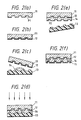
- a transparent substrate 11 carrying first recording pits P1 is prepared.
- the transparent substrate 11 is formed conventionally by injection molding a transparent resin, such as PMMA, PC, or the like, using a nickel stamper (not shown) on the surface of which pits P1 are arranged spirally or concentrically. As a result, the pit pattern of the nickel stamper is transferred onto the transparent substrate 11 as the first pits P1.
- silicon (Si) is evaporated onto the surface of the substrate 11 carrying the pits P1 by use of a vacuum evaporation apparatus so as to form a reflecting layer 12.
- the first reflecting layer 12 of silicon is formed on the transparent substrate 11.
- a transparent stamper 13 is prepared by conventional methods and mounted on a conventional transfer apparatus.
- the transparent stamper 13 is made of glass or plastic having a radiation transmitting property so as to be able to transmit light in a wavelength band necessary to harden a radiation setting resin 14 which is to be applied in the following step.
- the transparent stamper 13 has second recording pits P2 arranged spirally or concentrically on the surface thereof.
- the transparent stamper 13 is mounted on the transfer apparatus with the pit surface facing upward as shown in Fig. 1(c).
- a liquid radiation setting resin 14 is fed onto the pit surface of the transparent stamper 13.
- the transparent substrate 11 is then placed on the pit surface of the transparent stamper 13 through the liquid radiation setting resin 14 with the first reflecting layer 12 of the transparent substrate 11 facing downward.
- the radiation setting resin 14 will be held between the first reflecting layer 12 and the transparent stamper 13 (Fig. 1(d)).
- the first reflecting layer 12 is irradiated with radiation from the transparent stamper 13 side, that is, from the underside in the drawing, so as to harden the radiation setting resin 14.
- the hardened resin will conform its lower side to the pattern of second pits P2.
- the transparent stamper 13 is peeled off from the layer of the radiation setting resin 14, as shown in Fig. 1(e).
- a protecting layer 16 of a radiation setting resin is laminated onto the second reflecting layer 15 in order to protect the second reflecting layer 15, thereby obtaining an optical disk having a lamination of first and second reflecting layers 12 and 15 which differ from one another in their respective reflection light bands.
- the two pit patterns may be read separately by optical beams of different wavelength. For example, light which will reflect from one of the reflecting layers will pass through the other reflecting layer.
- the first reflecting layer 12 is made of silicon.
- a light beam of 400 nm wavelength directed from the top of the laminated layer will be reflected by the layer 12, and thereby will carry the information of pit pattern P1.
- the second reflecting layer of the above embodiment is aluminum.
- a light beam of not less than 800 nm wavelength directed from the top of the laminated layers will pass through the first reflecting layer 12 and be reflected by the second reflecting layer 15, and thereby will carry the information of pit pattern P2.
- the reflecting layers are made to be different in reflection light band from each other. Further, by adjusting the thickness of the first and second reflecting layers 12 and 15 in the evaporation step or in the sputtering step, it is possible to make the layers different from each other in light transmitting property.
- Figs. 1(a) to 1(f) may be repeated by use of reflecting-layer materials which are different in reflection light band from each other, so that an optical disk having two or more reflecting layers can be obtained.
- FIG. 2(a) A second embodiment of the invention is shown in Figs. 2(a) to 2(f).
- a transparent substrate 11 carrying first recording pits P1 is prepared.
- the transparent substrate 11 is the same as that in the first embodiment.
- a dielectric multi-layer reflecting layer is formed on the surface of the substrate 11.
- a first reflecting layer 12 having a first reflection light band is formed on the transparent substrate 11.
- the first reflecting layer is a dielectric multi-layer reflecting layer which reflects light of 800 nm while allowing light of other wavelengths, for example, not more than 600 nm, to pass therethrough.
- a stamper 13 having second recording pits arranged spirally or concentrically on the surface thereof is mounted on a transfer apparatus with the pit surface facing upward as shown in Fig. 2(c).
- a liquid radiation setting resin 14 is applied to the pit surface of the stamper 13.
- the transparent substrate 11 is then mounted on the pit surface of the stamper 13 through the liquid radiation setting resin 14 with the first reflecting layer 12 of the transparent substrate 11 facing downward.
- the radiation setting resin 14 is held between the first reflecting layer 12 and the stamper 13 (Fig. 2(d)).
- the first reflecting layer 12 is irradiated with radiation from the transparent substrate 11 side, that is, from the upper side in the drawing, so as to harden the radiation setting resin 14 to thereby form a transparent layer.
- the pits arranged on the stamper 13 are transferred as second pits P2 onto the transparent layer 14 of the hardened radiation setting resin.
- the stamper 13 is peeled off from the transparent layer 14 of the radiation setting resin.
- a dielectric multi-layer reflecting layer 15 is formed on the pits P2 carrying surface of the radiation setting resin 14 by use of the vacuum evaporation apparatus.
- the second reflecting layer 15 having a second reflection light band is formed as a lamination on the radiation setting resin 14.
- the second reflecting layer is a dielectric multi-layer reflecting layer which reflects laser light having a wavelength different from that of the first reflecting layer and allows light having the other wavelength to transmit therethrough.
- Figs. 2(c) to 2(f) may be repeated, thereby obtaining an optical disk having more than two reflecting layers.
- a protecting layer 16 of radiation setting resin is laminated on the last reflecting layer in order to protect the last reflecting layer, thereby obtaining an optical disk having laminations of multiple reflecting layers which are different from each other in reflection light band.
- the dielectric multi-layer reflecting layer has a narrow reflection light band by alternately laminating ⁇ /4 films of a high-refractive-index material such as PbO2, ZrO2, TiO2, or the like and a low-refractive-index material such as SiO2, MgF2, Al2O3, or the like. Further, it is possible to make the reflection light selectivity high by suitably shifting the film thicknesses of the respective films of the reflecting layer or by combining two or three reflection light bands on the same plane.
- a high-refractive-index material such as PbO2, ZrO2, TiO2, or the like
- a low-refractive-index material such as SiO2, MgF2, Al2O3, or the like.
- the second embodiment of the optical disk having a structure in which the reflecting layers differ from each other in reflection light band are laminated one on one is characterized in that it is made possible to produce the foregoing optical disk by means of an ordinary non transparent stamper by using, as a reflecting layer, a dielectric layer which can sufficiently transmit radiation having a wavelength band in which a radiation setting resin can be hardened.
- the present invention since a plurality of the reflection layers which differ in their respective reflection light bands from each other are laminated, it is possible to obtain an optical information record carrier which is improved in recording density.
- a transparent stamper having radiation transmitting property is used and radiation setting resin is irradiated with radiation from the transparent stamper side so as to harden the radiation setting resin. Accordingly, it is possible to obtain an optical information record carrier having a plurality of reflecting layers which are laminated, that is, it is possible to make an optical information record carrier have a large capacity.
Landscapes
- Engineering & Computer Science (AREA)
- Manufacturing & Machinery (AREA)
- Mechanical Engineering (AREA)
- Optical Record Carriers And Manufacture Thereof (AREA)
- Manufacturing Optical Record Carriers (AREA)
Applications Claiming Priority (4)
| Application Number | Priority Date | Filing Date | Title |
|---|---|---|---|
| JP281823/88 | 1988-11-08 | ||
| JP28182388 | 1988-11-08 | ||
| JP20999/89 | 1989-01-30 | ||
| JP1020999A JPH0823941B2 (ja) | 1988-11-08 | 1989-01-30 | 光学式情報記録担体及びその製造方法 |
Publications (3)
| Publication Number | Publication Date |
|---|---|
| EP0368442A2 true EP0368442A2 (de) | 1990-05-16 |
| EP0368442A3 EP0368442A3 (de) | 1991-04-17 |
| EP0368442B1 EP0368442B1 (de) | 1995-04-12 |
Family
ID=26358007
Family Applications (1)
| Application Number | Title | Priority Date | Filing Date |
|---|---|---|---|
| EP89307379A Expired - Lifetime EP0368442B1 (de) | 1988-11-08 | 1989-07-20 | Optischer Informationsaufzeichnungsträger und Verfahren zu seiner Herstellung |
Country Status (4)
| Country | Link |
|---|---|
| US (1) | US5126996A (de) |
| EP (1) | EP0368442B1 (de) |
| JP (2) | JPH0823941B2 (de) |
| DE (1) | DE68922185T2 (de) |
Cited By (30)
| Publication number | Priority date | Publication date | Assignee | Title |
|---|---|---|---|---|
| EP0509423A1 (de) * | 1991-04-16 | 1992-10-21 | MITSUI TOATSU CHEMICALS, Inc. | Optischer Aufzeichnungsträger |
| EP0517490A3 (en) * | 1991-06-04 | 1993-03-03 | International Business Machines Corporation | Multiple data surface optical medium and data storage system |
| EP0549024A1 (de) * | 1991-12-12 | 1993-06-30 | Koninklijke Philips Electronics N.V. | Optischer Informationsträger |
| EP0658885A1 (de) * | 1993-12-15 | 1995-06-21 | International Business Machines Corporation | Optischer Datenspeicher |
| US5449590A (en) * | 1991-06-04 | 1995-09-12 | International Business Machines Corporation | Multiple data surface optical data storage system |
| US5487060A (en) * | 1991-06-04 | 1996-01-23 | International Business Machines Corporation | Multiple data surface data storage system and method |
| EP0694915A1 (de) * | 1994-07-26 | 1996-01-31 | Pioneer Electronic Corporation | Mehrlagige Aufzeichnungsplatte und Aufzeichnungs-/Wiedergabeeinrichtung zu ihrer Anwendung |
| WO1995034112A3 (en) * | 1994-06-08 | 1996-03-07 | Prima Ind Establishment | Dimer laser, method and apparatus for data transmission, method and apparatus for storing and reading data, method and apparatus for detecting diatomic molecules, and laser projection microscope |
| EP0737966A1 (de) * | 1995-04-11 | 1996-10-16 | Sony Corporation | Mehrschichtige optische Platte |
| US5586107A (en) * | 1991-06-04 | 1996-12-17 | International Business Machines Corporation | Multiple data surface optical data storage system |
| WO1997005608A1 (en) * | 1995-07-27 | 1997-02-13 | Minnesota Mining And Manufacturing Company | Method and apparatus for making an optical information record |
| EP0762406A1 (de) * | 1995-09-01 | 1997-03-12 | Balzers Aktiengesellschaft | Informationsträger, Verfahren zur Schichtherstellung und Anlagen hierfür |
| NL1001324C2 (nl) * | 1995-01-24 | 1997-03-21 | Samsung Electronics Co Ltd | Werkwijze en inrichting voor het aanbrengen van een meerlagig optisch registratiemedium. |
| US5644555A (en) * | 1995-01-19 | 1997-07-01 | International Business Machines Corporation | Multiple data surface magneto-optical data storage system |
| US5666344A (en) * | 1991-06-04 | 1997-09-09 | International Business Machines Corporation | Multiple data surface optical data storage system |
| EP0814469A1 (de) * | 1996-06-18 | 1997-12-29 | SANYO ELECTRIC Co., Ltd. | Optischer Aufzeichnungsträger zur Ueberprüfung der Kompatibilität einer optischen Abtastvorrichtung, sowie davon Gebrauch machendes Verfahren zur Ueberprüfung der Kompatibilität einer optischen Abtastvorrichtung |
| FR2750528A1 (fr) * | 1996-06-28 | 1998-01-02 | Thomson Multimedia Sa | Disque optique compatible a deux systemes de lecture differents |
| EP0833313A1 (de) * | 1996-09-26 | 1998-04-01 | Victor Company Of Japan, Limited | Doppelschichtige optische Platte, sowie Aufzeichnungs- und Herstellungsverfahren dafür |
| NL1001413C2 (nl) * | 1994-11-11 | 1998-10-20 | Samsung Electronics Co Ltd | Optisch meerlaagsregistratiemedium. |
| GB2327525A (en) * | 1997-07-21 | 1999-01-27 | Samsung Electronics Co Ltd | Optical disk |
| EP1031407A1 (de) * | 1999-02-23 | 2000-08-30 | ODME International B.V. | Ein Verfahren zur Herstellung einer Scheibe und eine so hergestellte Scheibe |
| EP0797194A3 (de) * | 1996-03-21 | 2000-12-13 | Kabushiki Kaisha Toshiba | Doppelschichtiger Informationsaufzeichnungsträger mit Informationsaufzeichnungsschichten |
| US6210609B1 (en) | 1996-09-27 | 2001-04-03 | Sony Corporation | Method of manufacturing optical recording medium |
| WO2003019541A1 (en) * | 2001-08-29 | 2003-03-06 | Koninklijke Philips Electronics N.V. | Optical storage medium and method of manufacturing same |
| EP1378898A1 (de) * | 2002-07-04 | 2004-01-07 | Pioneer Corporation | Durchsichtige Prägeplatte für das Prägen von mehrschichtigen optischen Aufzeichnungsmedien und Verfahren zur Herstellung eines mehrschichtigen optischen Aufzeichnungsmediums |
| FR2871614A1 (fr) * | 2004-06-10 | 2005-12-16 | Commissariat Energie Atomique | Procede de realisation d'un support d'enregistrement optique a plusieurs etages et support obtenu |
| EP1553577A4 (de) * | 2002-10-16 | 2007-11-21 | Matsushita Electric Industrial Co Ltd | Informationsaufzeichnungsmedium, prozess zu seiner herstellung und optische informationsaufzeichnungs- und wiedergabeeinrichtung |
| USRE40136E1 (en) * | 1995-04-11 | 2008-03-04 | Sony Corporation | Multilayer optical disk |
| CN100377240C (zh) * | 2001-05-01 | 2008-03-26 | Tdk株式会社 | 光信息媒体的制造方法 |
| EP2421104A1 (de) | 2010-08-17 | 2012-02-22 | Tyco Electronics Raychem BVBA | Kabeldurchführung |
Families Citing this family (48)
| Publication number | Priority date | Publication date | Assignee | Title |
|---|---|---|---|---|
| JP2788777B2 (ja) * | 1990-03-02 | 1998-08-20 | パイオニア株式会社 | 光ピックアップ |
| JPH0536128A (ja) * | 1990-12-20 | 1993-02-12 | Hitachi Ltd | 高密度情報記録媒体及びそれを用いた記録装置 |
| US5748598A (en) * | 1995-12-22 | 1998-05-05 | Massachusetts Institute Of Technology | Apparatus and methods for reading multilayer storage media using short coherence length sources |
| JP3266627B2 (ja) * | 1991-10-11 | 2002-03-18 | 株式会社日立製作所 | 情報再生装置 |
| US7286153B1 (en) | 1991-10-11 | 2007-10-23 | Hitachi, Ltd. | Three-dimensional recording and reproducing apparatus |
| US5563873A (en) * | 1992-11-26 | 1996-10-08 | Matsushita Electric Industrial Co., Ltd. | Multilayer optical disk and apparatus |
| US5757763A (en) * | 1994-07-12 | 1998-05-26 | Massachusetts Institute Of Technology | Optical information storage via amplitude modulation |
| US5540966A (en) * | 1994-08-05 | 1996-07-30 | Minnesota Mining And Manufacturing Company | Dual layer optical medium having partially reflecting thin film layer |
| KR100230245B1 (ko) * | 1995-01-24 | 1999-11-15 | 윤종용 | 다층 광 기록 매체의 제조방법 및 그 장치 |
| US5532998A (en) * | 1995-02-14 | 1996-07-02 | Serotech, Inc. | Optical spectroscopic information storage |
| JPH08235641A (ja) * | 1995-02-27 | 1996-09-13 | Sony Corp | 光学記録媒体とその製法 |
| US5708652A (en) * | 1995-02-28 | 1998-01-13 | Sony Corporation | Multi-layer recording medium and method for producing same |
| US5625609A (en) * | 1995-03-13 | 1997-04-29 | International Business Machines Corporation | Multiple data layer optical disk drive system with fixed aberration correction and optimum interlayer spacing |
| US6676791B1 (en) | 1995-03-24 | 2004-01-13 | Jvc Victor Company Of Japan, Ltd. | Multilayered optical information-recording media and process for manufacture thereof |
| JP3351164B2 (ja) * | 1995-03-24 | 2002-11-25 | 日本ビクター株式会社 | 光学的情報記録媒体の製造方法 |
| US6038208A (en) * | 1995-03-30 | 2000-03-14 | Victor Company Of Japan, Ltd. | Information recording disc recorded with signals at two different recording densities |
| US5764619A (en) * | 1995-04-07 | 1998-06-09 | Matsushita Electric Industrial Co., Ltd. | Optical recording medium having two separate recording layers |
| CN1937044B (zh) * | 1995-04-07 | 2011-04-13 | 松下电器产业株式会社 | 光信息重现设备 |
| JP3210549B2 (ja) * | 1995-05-17 | 2001-09-17 | 日本コロムビア株式会社 | 光情報記録媒体 |
| JP3008819B2 (ja) | 1995-05-31 | 2000-02-14 | 日本ビクター株式会社 | 光ディスク |
| JP3635588B2 (ja) * | 1995-09-19 | 2005-04-06 | パイオニア株式会社 | 光ディスクの製造方法及び多層光ディスク |
| US5640382A (en) * | 1995-12-19 | 1997-06-17 | Imation Corp. | Dual layer optical medium having partially reflecting metal alloy layer |
| US5942302A (en) * | 1996-02-23 | 1999-08-24 | Imation Corp. | Polymer layer for optical media |
| US6678237B1 (en) | 1997-03-27 | 2004-01-13 | Imation Corp. | Dual layer optical storage medium having partially reflecting layer comprising amorphous selenium |
| US6628603B1 (en) | 1997-03-27 | 2003-09-30 | Imation Corp. | Dual layer optical storage medium having partially reflecting layer comprising antimony sulfide |
| US6214412B1 (en) | 1998-05-19 | 2001-04-10 | First Light Technologies, Inc. | System and method for distributing a resin disposed between a top substrate and a bottom substrate |
| US6106657A (en) * | 1998-05-19 | 2000-08-22 | First Light Technology, Inc. | System and method for dispensing a resin between substrates of a bonded storage disk |
| US6103039A (en) | 1997-11-12 | 2000-08-15 | First Light Technology, Inc. | System and method for thermally manipulating a combination of a top and bottom substrate before a curing operation |
| US6352612B1 (en) | 1998-05-19 | 2002-03-05 | Steag Hamatech, Inc. | System for forming bonded storage disks with low power light assembly |
| US6254809B1 (en) | 1998-05-19 | 2001-07-03 | Steag Hamatech, Inc. | System and method for curing a resin disposed between a top and bottom substrate with thermal management |
| US6098272A (en) * | 1998-05-19 | 2000-08-08 | First Light Technology, Inc. | System for maintaining concentricity of a combination of a top and bottom substrate during the assembly of a bonded storage disk |
| JPH11296904A (ja) | 1998-04-03 | 1999-10-29 | Toshiba Corp | 情報記録媒体およびこれに用いられる樹脂基板の製造方法 |
| EP0957477A3 (de) | 1998-05-15 | 2003-11-05 | Matsushita Electric Industrial Co., Ltd. | Optisches Aufzeichnungsmedium, Verfahren und Vorrichtung zur Informationsaufzeichnung und -wiedergabe dafür |
| EP0984440A3 (de) * | 1998-09-04 | 2000-05-24 | Matsushita Electric Industrial Co., Ltd. | Vorrichtung zur Aberrationsdetektion und Gerät zur Aufnahme und Wiedergabe von optischer Information |
| TW591654B (en) * | 2000-09-12 | 2004-06-11 | Matsushita Electric Industrial Co Ltd | Manufacturing method of optical information recording medium |
| JP2003067984A (ja) | 2001-08-24 | 2003-03-07 | Toshiba Corp | 光ディスク製造方法とこれにより製造される光ディスク |
| JP2003091887A (ja) * | 2001-09-20 | 2003-03-28 | Tdk Corp | 多層光記録媒体の製造方法および多層光記録媒体製造装置 |
| JP2003099991A (ja) * | 2001-09-27 | 2003-04-04 | Tdk Corp | 光記録媒体の製造方法および光記録媒体製造装置 |
| JP2003123331A (ja) * | 2001-10-04 | 2003-04-25 | Tdk Corp | 多層光記録媒体の製造方法および多層光記録媒体 |
| US7497916B2 (en) | 2002-03-27 | 2009-03-03 | Panasonic Corporation | Method of manufacturing multilayer optical information recording medium |
| WO2004075469A2 (en) * | 2003-02-19 | 2004-09-02 | Dotcast Inc. | Joint, adaptive control of equalization, synchronization, and gain in a digital communications receiver |
| US7346160B2 (en) * | 2003-04-23 | 2008-03-18 | Michaelsen David L | Randomization-based encryption apparatus and method |
| TW200519936A (en) | 2003-12-08 | 2005-06-16 | Victor Company Of Japan | Optical recording medium |
| US20050238145A1 (en) * | 2004-04-22 | 2005-10-27 | Sbc Knowledge Ventures, L.P. | User interface for "how to use" application of automated self service call center |
| CN1324595C (zh) * | 2004-07-19 | 2007-07-04 | 精碟科技股份有限公司 | 制造光信息储存媒体的模具及光信息储存媒体的制造方法 |
| JP4758189B2 (ja) * | 2005-09-28 | 2011-08-24 | パナソニック株式会社 | ダイ |
| JP2007234092A (ja) * | 2006-02-28 | 2007-09-13 | Victor Co Of Japan Ltd | 光ディスク及び光ディスクの製造方法 |
| JP4621646B2 (ja) * | 2006-09-13 | 2011-01-26 | 株式会社東芝 | ホログラフィックデータストレージ媒体 |
Family Cites Families (17)
| Publication number | Priority date | Publication date | Assignee | Title |
|---|---|---|---|---|
| US4219704A (en) * | 1974-10-21 | 1980-08-26 | Eli S. Jacobs | Record playback apparatus for optical data records |
| US4179532A (en) * | 1976-04-09 | 1979-12-18 | Polygram Gmbh | Process for producing a disc-shaped information carrier which has information in the form of a beam-reflecting structure |
| NL7803069A (nl) * | 1978-03-22 | 1979-09-25 | Philips Nv | Meerlaags informatieschijf. |
| JPS5718458A (en) * | 1980-07-04 | 1982-01-30 | Nissan Motor Co Ltd | Glow plug control device in diesel engine |
| JPS5734738A (en) * | 1980-08-11 | 1982-02-25 | Matsushita Electric Industrial Co Ltd | Automatic charger |
| US4515877A (en) * | 1982-11-27 | 1985-05-07 | Basf Aktiengesellschaft | Image-recording materials and image-recording carried out using these to produce an optical mask |
| JPS6174149A (ja) * | 1984-09-20 | 1986-04-16 | Nec Corp | 光記録媒体 |
| JPS61175946A (ja) * | 1985-01-29 | 1986-08-07 | Victor Co Of Japan Ltd | 情報記録媒体製造方法 |
| JPH0789414B2 (ja) * | 1986-01-31 | 1995-09-27 | シャープ株式会社 | 光学記憶素子 |
| JPS6381639A (ja) * | 1986-09-26 | 1988-04-12 | Canon Inc | 光学的記録媒体用基盤の製造方法 |
| JPS63146244A (ja) * | 1986-12-10 | 1988-06-18 | Hitachi Ltd | 波長多重光記録装置 |
| JPS63102031U (de) * | 1986-12-22 | 1988-07-02 | ||
| EP0299073B1 (de) * | 1987-01-24 | 1995-11-29 | Dai Nippon Insatsu Kabushiki Kaisha | Optisches speichermedium und herstellung |
| JPS63220434A (ja) * | 1987-03-09 | 1988-09-13 | Matsushita Electric Ind Co Ltd | 光デイスクおよびその記録再生方法 |
| US4977064A (en) * | 1987-05-01 | 1990-12-11 | Mitsui Toatsu Chemicals, Incorporated | Optical recording medium and process for fabricating the same |
| GB2216675B (en) * | 1988-03-02 | 1992-07-22 | Fuji Photo Film Co Ltd | Multicolor heat-sensitive recording material |
| JPH06253325A (ja) * | 1993-03-02 | 1994-09-09 | Matsushita Electric Ind Co Ltd | 色信号輪郭補正装置 |
-
1989
- 1989-01-30 JP JP1020999A patent/JPH0823941B2/ja not_active Expired - Fee Related
- 1989-07-20 US US07/382,371 patent/US5126996A/en not_active Expired - Fee Related
- 1989-07-20 EP EP89307379A patent/EP0368442B1/de not_active Expired - Lifetime
- 1989-07-20 DE DE68922185T patent/DE68922185T2/de not_active Expired - Fee Related
-
1998
- 1998-10-22 JP JP10301513A patent/JPH11224439A/ja active Pending
Cited By (56)
| Publication number | Priority date | Publication date | Assignee | Title |
|---|---|---|---|---|
| US5369321A (en) * | 1991-04-16 | 1994-11-29 | Mitsui Toatsu Chemicals, Inc. | Optical recording medium |
| EP0509423A1 (de) * | 1991-04-16 | 1992-10-21 | MITSUI TOATSU CHEMICALS, Inc. | Optischer Aufzeichnungsträger |
| US5598398A (en) * | 1991-06-04 | 1997-01-28 | International Business Machines Corporation | Multiple data surface optical data storage system |
| US5905700A (en) * | 1991-06-04 | 1999-05-18 | International Business Machines Corporation | Multiple data layer optical disk with recorded information identifying the type of tracking |
| US5381401A (en) * | 1991-06-04 | 1995-01-10 | International Business Machines Corporation | Multiple data surface optical data storage system |
| US5410530A (en) * | 1991-06-04 | 1995-04-25 | International Business Machines Corporation | Multiple data surface optical data storage system |
| US5615186A (en) * | 1991-06-04 | 1997-03-25 | International Business Machines Corporation | Multiple data surface data storage system with holographic filter element |
| US5446723A (en) * | 1991-06-04 | 1995-08-29 | International Business Machines Corporation | Multiple data surface optical data storage system |
| US5449590A (en) * | 1991-06-04 | 1995-09-12 | International Business Machines Corporation | Multiple data surface optical data storage system |
| US5487060A (en) * | 1991-06-04 | 1996-01-23 | International Business Machines Corporation | Multiple data surface data storage system and method |
| US5745473A (en) * | 1991-06-04 | 1998-04-28 | International Business Machines Corporation | Multiple data layer optical disk with recorded information identifying the type of tracking |
| EP0517490A3 (en) * | 1991-06-04 | 1993-03-03 | International Business Machines Corporation | Multiple data surface optical medium and data storage system |
| US5513170A (en) * | 1991-06-04 | 1996-04-30 | International Business Machines Corporation | Multiple data surface optical data storage system |
| US5606546A (en) * | 1991-06-04 | 1997-02-25 | International Business Machines Corporation | Optical data storage medium with multiple writable data layers separated by dieletric layers |
| US5586107A (en) * | 1991-06-04 | 1996-12-17 | International Business Machines Corporation | Multiple data surface optical data storage system |
| US5666344A (en) * | 1991-06-04 | 1997-09-09 | International Business Machines Corporation | Multiple data surface optical data storage system |
| EP0549024A1 (de) * | 1991-12-12 | 1993-06-30 | Koninklijke Philips Electronics N.V. | Optischer Informationsträger |
| EP0658885A1 (de) * | 1993-12-15 | 1995-06-21 | International Business Machines Corporation | Optischer Datenspeicher |
| WO1995034112A3 (en) * | 1994-06-08 | 1996-03-07 | Prima Ind Establishment | Dimer laser, method and apparatus for data transmission, method and apparatus for storing and reading data, method and apparatus for detecting diatomic molecules, and laser projection microscope |
| EP0694915A1 (de) * | 1994-07-26 | 1996-01-31 | Pioneer Electronic Corporation | Mehrlagige Aufzeichnungsplatte und Aufzeichnungs-/Wiedergabeeinrichtung zu ihrer Anwendung |
| NL1001413C2 (nl) * | 1994-11-11 | 1998-10-20 | Samsung Electronics Co Ltd | Optisch meerlaagsregistratiemedium. |
| US5644555A (en) * | 1995-01-19 | 1997-07-01 | International Business Machines Corporation | Multiple data surface magneto-optical data storage system |
| NL1001324C2 (nl) * | 1995-01-24 | 1997-03-21 | Samsung Electronics Co Ltd | Werkwijze en inrichting voor het aanbrengen van een meerlagig optisch registratiemedium. |
| US5766717A (en) * | 1995-04-11 | 1998-06-16 | Sony Corporation | Multilayer optical disk |
| EP1168319A1 (de) * | 1995-04-11 | 2002-01-02 | Sony Corporation | Mehrschichtige optische Platte |
| US6241843B1 (en) | 1995-04-11 | 2001-06-05 | Sony Corporation | Multilayer optical disk |
| USRE40136E1 (en) * | 1995-04-11 | 2008-03-04 | Sony Corporation | Multilayer optical disk |
| US5989670A (en) * | 1995-04-11 | 1999-11-23 | Sony Corporation | Multilayer optical disk |
| EP0737966A1 (de) * | 1995-04-11 | 1996-10-16 | Sony Corporation | Mehrschichtige optische Platte |
| US6537637B2 (en) | 1995-04-11 | 2003-03-25 | Sony Corporation | Multilayer optical disk |
| WO1997005608A1 (en) * | 1995-07-27 | 1997-02-13 | Minnesota Mining And Manufacturing Company | Method and apparatus for making an optical information record |
| US5965228A (en) * | 1995-09-01 | 1999-10-12 | Balzers Aktiengesellschaft | Information carrier, method for producing same |
| WO1997009715A1 (de) * | 1995-09-01 | 1997-03-13 | Balzers Aktiengesellschaft | Informationsträger, verfahren zur schichtherstellung und anlagen hierfür |
| EP0762406A1 (de) * | 1995-09-01 | 1997-03-12 | Balzers Aktiengesellschaft | Informationsträger, Verfahren zur Schichtherstellung und Anlagen hierfür |
| EP0797194A3 (de) * | 1996-03-21 | 2000-12-13 | Kabushiki Kaisha Toshiba | Doppelschichtiger Informationsaufzeichnungsträger mit Informationsaufzeichnungsschichten |
| US5914926A (en) * | 1996-06-18 | 1999-06-22 | Sanyo Electric Co., Ltd. | Optical recording medium for checking compatibility of an optical pickup device and method of checking an optical pickup device using the same |
| EP0814469A1 (de) * | 1996-06-18 | 1997-12-29 | SANYO ELECTRIC Co., Ltd. | Optischer Aufzeichnungsträger zur Ueberprüfung der Kompatibilität einer optischen Abtastvorrichtung, sowie davon Gebrauch machendes Verfahren zur Ueberprüfung der Kompatibilität einer optischen Abtastvorrichtung |
| WO1998000842A1 (fr) * | 1996-06-28 | 1998-01-08 | Thomson Multimedia | Disque optique compatible a deux systemes de lecture differents |
| FR2750528A1 (fr) * | 1996-06-28 | 1998-01-02 | Thomson Multimedia Sa | Disque optique compatible a deux systemes de lecture differents |
| US6434107B1 (en) | 1996-06-28 | 2002-08-13 | Thomson Licensing S.A. | Optical disk compatible with two different reading systems |
| EP1381041A3 (de) * | 1996-06-28 | 2008-02-13 | THOMSON multimedia | Mit zwei verschiedenen Wiedergabesystemen kompatible optische Platte |
| US5844876A (en) * | 1996-09-26 | 1998-12-01 | Victor Company Of Japan, Ltd. | Double-layer optical disk, recording method and manufacturing method of this optical disk |
| EP0833313A1 (de) * | 1996-09-26 | 1998-04-01 | Victor Company Of Japan, Limited | Doppelschichtige optische Platte, sowie Aufzeichnungs- und Herstellungsverfahren dafür |
| US6210609B1 (en) | 1996-09-27 | 2001-04-03 | Sony Corporation | Method of manufacturing optical recording medium |
| GB2327525A (en) * | 1997-07-21 | 1999-01-27 | Samsung Electronics Co Ltd | Optical disk |
| US6517749B1 (en) | 1999-02-23 | 2003-02-11 | Otb Group B.V. | Method of producing a disc and a disc obtained by the method |
| EP1031407A1 (de) * | 1999-02-23 | 2000-08-30 | ODME International B.V. | Ein Verfahren zur Herstellung einer Scheibe und eine so hergestellte Scheibe |
| CN100377240C (zh) * | 2001-05-01 | 2008-03-26 | Tdk株式会社 | 光信息媒体的制造方法 |
| WO2003019541A1 (en) * | 2001-08-29 | 2003-03-06 | Koninklijke Philips Electronics N.V. | Optical storage medium and method of manufacturing same |
| EP1378898A1 (de) * | 2002-07-04 | 2004-01-07 | Pioneer Corporation | Durchsichtige Prägeplatte für das Prägen von mehrschichtigen optischen Aufzeichnungsmedien und Verfahren zur Herstellung eines mehrschichtigen optischen Aufzeichnungsmediums |
| EP1553577A4 (de) * | 2002-10-16 | 2007-11-21 | Matsushita Electric Industrial Co Ltd | Informationsaufzeichnungsmedium, prozess zu seiner herstellung und optische informationsaufzeichnungs- und wiedergabeeinrichtung |
| FR2871614A1 (fr) * | 2004-06-10 | 2005-12-16 | Commissariat Energie Atomique | Procede de realisation d'un support d'enregistrement optique a plusieurs etages et support obtenu |
| WO2006005827A1 (fr) * | 2004-06-10 | 2006-01-19 | Commissariat A L'energie Atomique | Procede de realisation d’un support d’enregistrement optique a plusieurs etages et support obtenu |
| US7909957B2 (en) | 2004-06-10 | 2011-03-22 | Commissariat A L'energie Atomique | Process for producing an optical recording medium with several stages and medium obtained thereby |
| KR101111937B1 (ko) * | 2004-06-10 | 2012-04-06 | 엠피오 인터내셔날 | 다중-스테이지 광학 기록 매체 및 그 제조 방법 |
| EP2421104A1 (de) | 2010-08-17 | 2012-02-22 | Tyco Electronics Raychem BVBA | Kabeldurchführung |
Also Published As
| Publication number | Publication date |
|---|---|
| DE68922185D1 (de) | 1995-05-18 |
| JPH0823941B2 (ja) | 1996-03-06 |
| DE68922185T2 (de) | 1995-11-09 |
| JPH02223030A (ja) | 1990-09-05 |
| EP0368442A3 (de) | 1991-04-17 |
| JPH11224439A (ja) | 1999-08-17 |
| US5126996A (en) | 1992-06-30 |
| EP0368442B1 (de) | 1995-04-12 |
Similar Documents
| Publication | Publication Date | Title |
|---|---|---|
| EP0368442B1 (de) | Optischer Informationsaufzeichnungsträger und Verfahren zu seiner Herstellung | |
| US5171392A (en) | Method of producing an optical information record carrier | |
| US4450553A (en) | Multilayer information disc | |
| US5708652A (en) | Multi-layer recording medium and method for producing same | |
| US5509991A (en) | Method of producing an optical disk having an integrated label layer | |
| US5846627A (en) | Method for writing and reading data on a multi-layer recordable interferometric optical disc and method for fabricating such | |
| US6537637B2 (en) | Multilayer optical disk | |
| JP3635588B2 (ja) | 光ディスクの製造方法及び多層光ディスク | |
| JP3581246B2 (ja) | 貼り合わせ型光ディスクの製造方法 | |
| US5645908A (en) | Multi-layer optical recording device | |
| KR19990007172A (ko) | 다층 광 디스크 | |
| EP1178475A2 (de) | Optisches Aufzeichnungsmedium | |
| KR0141181B1 (ko) | 다층 광 기록 매체 및 제조방법 | |
| JPH10222870A (ja) | 光記録媒体 | |
| JP2002334490A (ja) | 光学式情報記録担体の製造方法 | |
| JPH09147417A (ja) | 光学記録媒体およびその製造方法 | |
| CN1610940A (zh) | 多层光记录介质以及多层光记录介质的制造方法 | |
| JPH09265674A (ja) | 光記録媒体の製造方法および製造装置 | |
| JPH11283278A (ja) | 光記録媒体 | |
| JPH0954985A (ja) | 光デイスク及び光デイスクの製造方法 | |
| JP3671484B2 (ja) | 光学記録媒体 | |
| JP2005092927A (ja) | 多層光ディスク | |
| JPH08306085A (ja) | 多層構造光学記録媒体の製造方法 | |
| JPS59217244A (ja) | 情報信号記録円盤 | |
| KR100618999B1 (ko) | 고밀도 광디스크 |
Legal Events
| Date | Code | Title | Description |
|---|---|---|---|
| PUAI | Public reference made under article 153(3) epc to a published international application that has entered the european phase |
Free format text: ORIGINAL CODE: 0009012 |
|
| AK | Designated contracting states |
Kind code of ref document: A2 Designated state(s): DE FR GB NL |
|
| PUAL | Search report despatched |
Free format text: ORIGINAL CODE: 0009013 |
|
| AK | Designated contracting states |
Kind code of ref document: A3 Designated state(s): DE FR GB NL |
|
| 17P | Request for examination filed |
Effective date: 19911011 |
|
| 17Q | First examination report despatched |
Effective date: 19931207 |
|
| GRAA | (expected) grant |
Free format text: ORIGINAL CODE: 0009210 |
|
| AK | Designated contracting states |
Kind code of ref document: B1 Designated state(s): DE FR GB NL |
|
| REF | Corresponds to: |
Ref document number: 68922185 Country of ref document: DE Date of ref document: 19950518 |
|
| PGFP | Annual fee paid to national office [announced via postgrant information from national office to epo] |
Ref country code: GB Payment date: 19950710 Year of fee payment: 7 |
|
| PGFP | Annual fee paid to national office [announced via postgrant information from national office to epo] |
Ref country code: FR Payment date: 19950711 Year of fee payment: 7 |
|
| ET | Fr: translation filed | ||
| PGFP | Annual fee paid to national office [announced via postgrant information from national office to epo] |
Ref country code: DE Payment date: 19950725 Year of fee payment: 7 |
|
| PLBE | No opposition filed within time limit |
Free format text: ORIGINAL CODE: 0009261 |
|
| STAA | Information on the status of an ep patent application or granted ep patent |
Free format text: STATUS: NO OPPOSITION FILED WITHIN TIME LIMIT |
|
| 26N | No opposition filed | ||
| PG25 | Lapsed in a contracting state [announced via postgrant information from national office to epo] |
Ref country code: GB Effective date: 19960720 |
|
| GBPC | Gb: european patent ceased through non-payment of renewal fee |
Effective date: 19960720 |
|
| PG25 | Lapsed in a contracting state [announced via postgrant information from national office to epo] |
Ref country code: FR Effective date: 19970328 |
|
| PG25 | Lapsed in a contracting state [announced via postgrant information from national office to epo] |
Ref country code: DE Effective date: 19970402 |
|
| REG | Reference to a national code |
Ref country code: FR Ref legal event code: ST |
|
| PGFP | Annual fee paid to national office [announced via postgrant information from national office to epo] |
Ref country code: NL Payment date: 20060716 Year of fee payment: 18 |
|
| NLV4 | Nl: lapsed or anulled due to non-payment of the annual fee |
Effective date: 20080201 |
|
| PG25 | Lapsed in a contracting state [announced via postgrant information from national office to epo] |
Ref country code: NL Free format text: LAPSE BECAUSE OF NON-PAYMENT OF DUE FEES Effective date: 20080201 |