EP0368469A1 - Systèmes de communication numérique - Google Patents
Systèmes de communication numérique Download PDFInfo
- Publication number
- EP0368469A1 EP0368469A1 EP19890310156 EP89310156A EP0368469A1 EP 0368469 A1 EP0368469 A1 EP 0368469A1 EP 19890310156 EP19890310156 EP 19890310156 EP 89310156 A EP89310156 A EP 89310156A EP 0368469 A1 EP0368469 A1 EP 0368469A1
- Authority
- EP
- European Patent Office
- Prior art keywords
- data
- mhz
- clock
- bit
- synch
- Prior art date
- Legal status (The legal status is an assumption and is not a legal conclusion. Google has not performed a legal analysis and makes no representation as to the accuracy of the status listed.)
- Withdrawn
Links
Images


Classifications
-
- H—ELECTRICITY
- H04—ELECTRIC COMMUNICATION TECHNIQUE
- H04L—TRANSMISSION OF DIGITAL INFORMATION, e.g. TELEGRAPHIC COMMUNICATION
- H04L1/00—Arrangements for detecting or preventing errors in the information received
- H04L1/24—Testing correct operation
- H04L1/242—Testing correct operation by comparing a transmitted test signal with a locally generated replica
- H04L1/243—Testing correct operation by comparing a transmitted test signal with a locally generated replica at the transmitter, using a loop-back
-
- G—PHYSICS
- G06—COMPUTING OR CALCULATING; COUNTING
- G06F—ELECTRIC DIGITAL DATA PROCESSING
- G06F13/00—Interconnection of, or transfer of information or other signals between, memories, input/output devices or central processing units
- G06F13/38—Information transfer, e.g. on bus
- G06F13/42—Bus transfer protocol, e.g. handshake; Synchronisation
- G06F13/4204—Bus transfer protocol, e.g. handshake; Synchronisation on a parallel bus
- G06F13/4208—Bus transfer protocol, e.g. handshake; Synchronisation on a parallel bus being a system bus, e.g. VME bus, Futurebus, Multibus
- G06F13/4213—Bus transfer protocol, e.g. handshake; Synchronisation on a parallel bus being a system bus, e.g. VME bus, Futurebus, Multibus with asynchronous protocol
Definitions
- This invention relates to digital communications systems and is more particularly concerned with a communications device for use in such a system.
- Digital communications systems are useful in a variety of complex control systems, for example automatic control systems for controlling military aircraft which require 'fly-by-wire' systems in order to enable them to be flown.
- automatic control systems for controlling military aircraft which require 'fly-by-wire' systems in order to enable them to be flown.
- the need, in this and other areas of application, to handle large quantities of data, in real time, and with great reliability, has fuelled the development of such systems.
- Synchronisation of data throughput between control lanes included assigning cross consolidation techniques prior to each control task being executed. Synchronisation allowed exchange of parameters between lanes at exactly the time they were required. This removed the problem of time skew occurring and so eased the task of cross consolidation.
- the voter monitor software designed to increase reliability by taking the votes of a plurality of outputs before executing action based on those outputs, and which must therefore be executed before the control law algorithm, resulted in a significant hardware overhead if the overall iteration rate was to be adequately fast.
- the synchronisation of microprocessors also leads to an increased probability of common mode failure between lanes.
- the complexity of both the hardware and software design leads to an increased probability of a degradation in synchronisation between processors due to a single software bug or hardware failure.
- a synchronous serial (single processor) system has the advantage of eliminating time skew problems but has the disadvantages of slow data throughput, complex software executives, increased probability of common mode failure and increased hardware overheads.
- AMPS Asynchronous Multi p rocessor System
- the AMPS concept relies on a number of identical processing modules, running in parallel with one another but asynchronously.
- the asynchronous processing enables any processor to perform its control task at the maximum possible rate.
- the latest i.e. the most recent data
- the latest will be stored as a variable which can be accessed at any time by another asynchronous processor.
- Time skew occurs in asynchronous systems because the input signal sampling occurs at different instants in time for each processor.
- Present day microprocessors are fast enough to sample and process data in a short iteration time, such that time skew is minimal and therefore degradation of the control output is no longer acute.
- computing modules are standardised to ease fault hardware inspection as well as reduce design, development and manufacturing costs.
- VLSI Very Large Scale Integration
- GCM General Computing Module
- an asynchronous communications device including a dual port memory, means for inputting data into the dual port memory, and means for outputting data from the dual port memory, the device being configured to operate in a receive mode or a transmit mode according to its connection in a communications system.
- the device can also function as a data concentrator to access a number of external Dual Port Memories (DPMs) and retransmit the data.
- DPMs Dual Port Memories
- any digital clock extraction circuit implemented needs to operate at a minimum rate four times that of the data signal frequency.
- a data signal frequency of 20 MHz is used, it is difficult to implement effectively a clock frequency of 80 MHz.
- a method of producing a clock frequency by utilising four clock pulses with their rising edges 90° apart.
- Such a method of implementing the clock frequency overcomes the disadvantage caused by the receiver and transmitter clock frequencies drifting apart during the course of a message in a phase locked loop whilst locking onto the synch. pulse. Furthermore it overcomes the problem associated with clock extraction directly from data i.e. the clocks only being present when the data is present.
- the data within these four shift registers is changing at 80 MHz, therefore effectively sampling the incoming data at that rate.
- the clock extraction circuit will therefore need to latch onto one of the patterns produced in the set of shift registers, and from that pattern, align the system clock with the data.
- the synch. pulse chosen for the AMPS protocol is three bits wide, that is one and a half bits high, followed by one and a half bits low. The reason for using such a pulse is twofold:
- Patterns B, C and D contain 'don't care' states because these occur past the end of the synch. pulse, which is detected simply by the presence of six 'ones' or 'zeros'.
- each pattern Associated with each pattern are two particular system clocks, which are aligned with both half bits of the data word i.e. pattern A has clock 0 ⁇ 2 aligned with the first half bit and clock 0 ⁇ 4 with the second half bit.
- Pattern B has clock 0 ⁇ 1 and 0 ⁇ 3 etc.
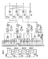
- the four pattern detectors are a set of simple combinational logic gates as shown in Figure 1. Once a set synch. pulse is detected then the output of one of the sets of combinational logic gates goes high for 12.5 ns. It is this short pulse which is used to latch the clock associated with that pattern through to the next stage of the receiver.
- Both 0 ⁇ 2 and 0 ⁇ 4 are enabled for a total of twenty-nine bits (to the twelfth 80 MHz clock pulse on the preceding synch.) where crossover between clock signals will occur if the data needs to be resynched; for instance, if 'glitching' or time skew has occurred, and the shift registers clock in a different synch pattern, then 0 ⁇ 2 and 0 ⁇ 4 must be disabled before latching through the two new clocks. This is achieved by applying a 'clear' signal to all D-type flip-flops via a three-input OR gate as shown in Figure 1. Careful design of the pattern detectors is required in order to equalise critical path lengths, as timing considerations are critical through the various logic gates and latches.
- Clock 0 ⁇ 2 is used to latch the following address, data and parity bits into the twenty-six bit shift register A.
- Each negative transition of 0 ⁇ 2 also clocks a 0-26 bit counter which, on the negative transition of the twenty-sixth pulse, latches the data bits present at the output of the shift register.
- the message format comprises twenty-nine bits which are divided as:- synch. pulse 3 bits address tag 8 bits address parity 1 bit data word 16 bits data parity 1 bit
- the device is capable of transmitting a variable number of different message lengths from 0 to 256 words per message. A transmission rate of 680 kHz is maintainable.
- both half bits are at a constant value, when an error occurs in the Manchester coded data, the output of the exclusive NOR gate is used to reset the twenty-six bit shift register A.
- the 0-26 bit counter is also reset by an error in the data. This ensures that data is not transmitted through to the internal DPM of the chip if that data contains an error. This check is performed on the address, data and parity bits.
- the maximum permissible switching time that can be tolerated between a particular synch. pattern being detected, and the switching of its associated clock signals is 12.5 ns.
- the overall switching speed may be reduced to 4 ns, thus rendering any lengthening of the synch. pulse unprofitable.
- each card includes eight communications chips, which operate to receive and concentrate data, process it, voting where necessary, and to issue, via a transmitter chip, instructions to actuators to operate control surfaces. Of the eight chips, seven are configured as receivers (Rx) and one as a transmitter (Tx).
- Rx receivers
- Tx transmitter
- tri-state latch B When the communications chip is configured as a receiver (Rx), tri-state latch B is enabled and tri-state latch A disabled (see Figure 4).
- the eight address bits A0 to A7 associated with each data word are latched through to the DPM via uni-directional non-inverting buffers. These address bits are used to write each data word into a specific location in memory.
- the 'write' signal from the receiver goes 'high' then the data bits D0 to D15 are latched through a bi-directional buffer (see Figure 5) to the DPM.
- latch A When configured as a transmitter, latch A is enabled and latch B disabled.
- the address bits are again latched through non-inverting buffers to the DPM, whilst the bi-directional buffers are configured via the 'Tx' and 'read' signal to accept data being read from the DPM.
- sixteen bit data is retrieved from DPM encoded into a Manchester format and transmitted in frame lengths of up to 256 words.
- Each word will consist of a three bit synch. pulse used by the receiver to synchronise data with the system clock, an eight bit address tab, sixteen bit data word and one bit address and data parity.
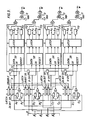
- the transmitter encoding circuitry is outlined in Figure 6.
- the 0-29 bit counter is clocked by a 20 MHz system clock (i.e. 0 ⁇ 2) after being enabled via the Rx/Tx pin.
- output '0' goes 'high' shift registers A and B are enabled and are clocked by 0 ⁇ 2 and 0 ⁇ 2 respectively.
- Both outputs (which are shown in Figure 7) are combined by an OR gate to produce the three bit synch. pulse output and both shift registers are disabled on the rising edge of output '3' from the 0-29 bit counter.
- the address counter shown is incremented on the negative transition of bit 29, and is used to address the 4k bit DPM.
- the DPM 'read' line is enabled on the positive edge of output '0', after which the address and data bits are passed through parity generators to a twenty-six bit wide latch.
- the address and data bits are latched on the positive transition of output '2' from the 0-29 bit counter, via a D-type flip-flop.
- shift register C On the positive edge of output '3', shift register C is enabled which allows the parallel address and data bits to be clocked out in a serial format by 0 ⁇ 2. Shift register C is disabled on the positive edge of output '0', therefore ensuring that data is only output at the end of the three bit synch. pulse.
- the information output from shift register C is encoded into a Manchester format via the two-input multiplexer shown.
- the positive transition of 0 ⁇ 2 transmits the data in the first half of each bit, whilst the negative transition clocks through the complement of this data, to form a Manchester protocol.
- the device has a built-in test facility for both transmit and receive modes. For the receive mode, every sixteenth word in a 256 word frame is clocked into a twenty-six bit test shift register at the beginning of the receive circuitry. This same word is then clocked through to the output of the DPM buffer, to a twenty-four bit comparator. The original word stored in the test shift register is then compared with the latter, and if they differ an error is deemed to have occurred in that position of the chip circuitry and an error flag set 'high'.
- the four 'write' signals from the receiver are used to clock a 0-16 counter via an OR gate.
- the counter output equals sixteen all four twenty-six bit test shift registers are enabled (see Figure 8). Data is then latched into the shift register enabled via the system clock, with the synch. pulse being detected and reset.
- output '26' from the 0-26 bit counter goes 'low' then the test shift register is disabled and the output latched through to the comparator.
- test philosophy is adopted for the transmit circuitry with test words being clocked into a twenty-six bit latch at the beginning of the circuit. The same word is then clocked into a shift register at the output and compared with the original latched bits to identify any faults occuring in the transmit circuitry.
- Both receive and transmit built in test are therefore in continuous operation.
- the processor interface and DPM access circuitry can be tested by external built-in test circuitry on power-up. A failure in that part of the device would therefore be flagged, before any 'on-chip' built-in test takes place.
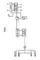
- the general purpose processor interface shown in Figure 9 will enable a number of microprocessors to interface directly to the DPM whether in transmit or receive mode. It also contains the circuitry required to configure the chip as a data concentrator.
- the address and data bi-directional buffers are enabled such that the address lines are configured from the processor, and the data lines to the processor.
- the 0-256 bit address counter is disabled and the address latch enabled.
- both address and data buffers are configured to receive information from the processor.
- the data concentrator circuitry is enabled by setting both the 'DC' and W/R pins 'high'. This enables the internal counter to output 0-256 address bytes to an external remapping PROM. A number of external receive chips may then be accessed, and their stored information read back to the internal DPM of the data concentrator. The information received is then transmitted in a serial format from the transmit circuitry of the chip.
Landscapes
- Engineering & Computer Science (AREA)
- Theoretical Computer Science (AREA)
- Physics & Mathematics (AREA)
- General Engineering & Computer Science (AREA)
- General Physics & Mathematics (AREA)
- Computer Networks & Wireless Communication (AREA)
- Signal Processing (AREA)
- Synchronisation In Digital Transmission Systems (AREA)
Applications Claiming Priority (2)
| Application Number | Priority Date | Filing Date | Title |
|---|---|---|---|
| GB8823336 | 1988-10-05 | ||
| GB888823336A GB8823336D0 (en) | 1988-10-05 | 1988-10-05 | Digital communications systems |
Publications (1)
| Publication Number | Publication Date |
|---|---|
| EP0368469A1 true EP0368469A1 (fr) | 1990-05-16 |
Family
ID=10644732
Family Applications (1)
| Application Number | Title | Priority Date | Filing Date |
|---|---|---|---|
| EP19890310156 Withdrawn EP0368469A1 (fr) | 1988-10-05 | 1989-10-04 | Systèmes de communication numérique |
Country Status (3)
| Country | Link |
|---|---|
| US (1) | US5058143A (fr) |
| EP (1) | EP0368469A1 (fr) |
| GB (1) | GB8823336D0 (fr) |
Families Citing this family (2)
| Publication number | Priority date | Publication date | Assignee | Title |
|---|---|---|---|---|
| JPH0764955A (ja) * | 1993-06-30 | 1995-03-10 | Mitsubishi Electric Corp | 半導体集積回路装置 |
| US5809220A (en) * | 1995-07-20 | 1998-09-15 | Raytheon Company | Fault tolerant distributed control system |
Citations (1)
| Publication number | Priority date | Publication date | Assignee | Title |
|---|---|---|---|---|
| EP0200352A2 (fr) * | 1985-03-25 | 1986-11-05 | British Aerospace Public Limited Company | Système de commande à calculateur |
Family Cites Families (11)
| Publication number | Priority date | Publication date | Assignee | Title |
|---|---|---|---|---|
| US4716575A (en) * | 1982-03-25 | 1987-12-29 | Apollo Computer, Inc. | Adaptively synchronized ring network for data communication |
| SE430740B (sv) * | 1982-04-26 | 1983-12-05 | Ellemtel Utvecklings Ab | Anordning for synkronisering av overforing av information pa en enkelriktad buss |
| US4596026A (en) * | 1983-05-09 | 1986-06-17 | Raytheon Company | Asynchronous data clock generator |
| US4670878A (en) * | 1984-08-14 | 1987-06-02 | Texas Instruments Incorporated | Column shift circuitry for high speed testing of semiconductor memory devices |
| US4757503A (en) * | 1985-01-18 | 1988-07-12 | The University Of Michigan | Self-testing dynamic ram |
| JPS6378400A (ja) * | 1986-09-19 | 1988-04-08 | Fujitsu Ltd | Ram試験方式 |
| JPH0728280B2 (ja) * | 1986-10-17 | 1995-03-29 | 富士通株式会社 | 多重マルチフレ−ム同期検出回路 |
| AR242878A1 (es) * | 1986-11-27 | 1993-05-31 | Siemens Ag | Disposicion de circuito para derivar una senal de reloj auxiliar de datos a partir de la frecuencia y/o de la fase de reloj de una senal digital sincronica o plesiocronica. |
| US4827476A (en) * | 1987-04-16 | 1989-05-02 | Tandem Computers Incorporated | Scan test apparatus for digital systems having dynamic random access memory |
| CA1289199C (fr) * | 1987-09-19 | 1991-09-17 | Masaaki Kawai | Circuit dephaseur |
| US4876699A (en) * | 1988-05-06 | 1989-10-24 | Rockwell International Corporation | High speed sampled data digital phase detector apparatus |
-
1988
- 1988-10-05 GB GB888823336A patent/GB8823336D0/en active Pending
-
1989
- 1989-10-04 EP EP19890310156 patent/EP0368469A1/fr not_active Withdrawn
- 1989-10-05 US US07/416,789 patent/US5058143A/en not_active Expired - Fee Related
Patent Citations (1)
| Publication number | Priority date | Publication date | Assignee | Title |
|---|---|---|---|---|
| EP0200352A2 (fr) * | 1985-03-25 | 1986-11-05 | British Aerospace Public Limited Company | Système de commande à calculateur |
Non-Patent Citations (3)
| Title |
|---|
| GaAs IC SYMPOSIUM, TECHNICAL DIGEST, Grenelefe, Florida, 28th - 30th October 1986, pages 151-154, IEEE, New York, US; H. NAKAMURA et al.: "ZGHz multiplexer and demultiplexer using DCFL/SBFL circuit and the precise Vth control process" * |
| IBM TECHNICAL DISCLOSURE BULLETIN, vol. 27, no. 3, August 1984, pages 1662-1663, New York, US; J.T. NOWELL et al.: "Diagnostic wrap of an SDLC adapter with a single DMA channel" * |
| IEEE/AIAA 7TH DIGITAL AVIONICS SYSTEMS CONFERENCE, Forth worth, Texas, 13th 16th October 1986, pages 507-514, IEEE, New York, US; D.P. GLUCH et al.: "Fault-tolerance in distributed digital fly-by-wire flight control systems" * |
Also Published As
| Publication number | Publication date |
|---|---|
| GB8823336D0 (en) | 1989-07-05 |
| US5058143A (en) | 1991-10-15 |
Similar Documents
| Publication | Publication Date | Title |
|---|---|---|
| US5349654A (en) | Fault tolerant data exchange unit | |
| EP0384177B1 (fr) | Synchronisation automatique à vernier de flux de données décalées | |
| US5768529A (en) | System and method for the synchronous transmission of data in a communication network utilizing a source clock signal to latch serial data into first registers and a handshake signal to latch parallel data into second registers | |
| Simpson | Four-slot fully asynchronous communication mechanism | |
| US4635261A (en) | On chip test system for configurable gate arrays | |
| US5271023A (en) | Uninterruptable fault tolerant data processor | |
| US20030035369A1 (en) | Communication system and communication control method | |
| KR100361856B1 (ko) | 통신시스템 및 통신제어방법 | |
| US9594715B2 (en) | Integrated circuit devices, systems and methods having automatic configurable mapping of input and/or output data connections | |
| Gustavson et al. | Local-area multiprocessor: the scalable coherent interface | |
| McConnel et al. | Synchronization and voting | |
| US5058143A (en) | Digital communications systems | |
| KR20070070662A (ko) | 초소형 위성용 데이터제어 자동복구 시스템 | |
| Smith Jr et al. | Development and evaluation of a fault-tolerant multiprocessor (FTMP) computer. Volume 1: FTMP principles of operation | |
| CN118708538A (zh) | 一种存算一体芯粒的集成系统 | |
| Standeven et al. | Hardware voter for fault-tolerant transputer systems | |
| Abler | A network element based fault tolerant processor | |
| CN121165913B (zh) | 锁步核处理器、锁步核复位电路及电子设备 | |
| CN217213701U (zh) | 用于多时钟切换的电路、fpga和电子设备 | |
| US5418794A (en) | Error determination scan tree apparatus and method | |
| Dür | Fault-tolerant GALS architecture based on pausable clocking | |
| Prizant | High speed communicator for fault tolerant systems | |
| JPH01137353A (ja) | インタフエース回路 | |
| Yao et al. | State synchronization technique based on present input and healthy state for repairable TMR systems | |
| SU1293861A1 (ru) | Устройство дл контрол дублированной системы |
Legal Events
| Date | Code | Title | Description |
|---|---|---|---|
| PUAI | Public reference made under article 153(3) epc to a published international application that has entered the european phase |
Free format text: ORIGINAL CODE: 0009012 |
|
| AK | Designated contracting states |
Kind code of ref document: A1 Designated state(s): DE FR GB IT NL |
|
| 17P | Request for examination filed |
Effective date: 19900605 |
|
| RAP3 | Party data changed (applicant data changed or rights of an application transferred) |
Owner name: BRITISH AEROSPACE PUBLIC LIMITED COMPANY |
|
| 17Q | First examination report despatched |
Effective date: 19930708 |
|
| STAA | Information on the status of an ep patent application or granted ep patent |
Free format text: STATUS: THE APPLICATION IS DEEMED TO BE WITHDRAWN |
|
| 18D | Application deemed to be withdrawn |
Effective date: 19940119 |