EP0370814A2 - Verriegelungskomparator mit Unterdrückung der Nullpunktabweichung - Google Patents
Verriegelungskomparator mit Unterdrückung der Nullpunktabweichung Download PDFInfo
- Publication number
- EP0370814A2 EP0370814A2 EP89312182A EP89312182A EP0370814A2 EP 0370814 A2 EP0370814 A2 EP 0370814A2 EP 89312182 A EP89312182 A EP 89312182A EP 89312182 A EP89312182 A EP 89312182A EP 0370814 A2 EP0370814 A2 EP 0370814A2
- Authority
- EP
- European Patent Office
- Prior art keywords
- transistor
- transistors
- electrode
- voltage
- latching comparator
- Prior art date
- Legal status (The legal status is an assumption and is not a legal conclusion. Google has not performed a legal analysis and makes no representation as to the accuracy of the status listed.)
- Granted
Links
Images

Classifications
-
- H—ELECTRICITY
- H03—ELECTRONIC CIRCUITRY
- H03K—PULSE TECHNIQUE
- H03K3/00—Circuits for generating electric pulses; Monostable, bistable or multistable circuits
- H03K3/02—Generators characterised by the type of circuit or by the means used for producing pulses
- H03K3/353—Generators characterised by the type of circuit or by the means used for producing pulses by the use, as active elements, of field-effect transistors with internal or external positive feedback
- H03K3/356—Bistable circuits
- H03K3/356017—Bistable circuits using additional transistors in the input circuit
- H03K3/356034—Bistable circuits using additional transistors in the input circuit the input circuit having a differential configuration
Definitions
- the present invention relates, in general, to a latching comparator. More particularly, the invention relates to an offset cancel latching comparator which may cancel an offset voltage caused by transistor mismatch in the comparator.
- latching comparators comparing two input voltages have many applications such as analog to digital converters used in VCR.
- Such comparator includes a pair of differential inputs for receiving two input voltages to be compared, a pair of transistors differentially driven by the differential input voltages, and a pair of differential outputs.
- the differential output voltage undesirably does not become zero, that is, there exists a nonzero input offset voltage which must be applied to drive the output voltage difference to zero.
- This offset voltage is unwanted because it leads to malfunction or wrong outputs as explained later in more detail.
- the offset error is serious in latching comparators applied to A/D converter, because the comparators must respond at high speed to small signal inputs. Therefore reducing the offset voltage is desired in many applications.
- the predominant source of the offset error is the mismatch of the transistor pair mainly due to a wafer process inaccuracy such as gate length variation, gate width variation, oxide thickness variation, etc. Accordingly, it is possible to reduce the offset voltage by using a large geometric size which makes it easier to match the transistor pair.
- the large geometry causes slow response and requires very wide area on the silicon resulting in the die cost increasing.
- an offset cancel latching comparator comprising first and second input terminals(IN, VX); first and second output terminals(DN, DP); first and second transistors(Q2, Q3) forming a first differential pair, control electrodes of the first and second transistors being connected to the first and second input terminals respectively, first electrodes of the first and second transistors both being connected to a current source(Q1), and a second electrode of the second transistor being connected to the first output terminal and, a second electrode of the first transistor being connected to the second output terminal; third and fourth transistors(Q6, Q7) forming a second differential pair, first electrodes of the third and fourth transistors both being connected to a voltage supply(VDD), a second electrode of the third transistor being connected to the second electrode of the first transistor, and a second electrode of the fourth transistor being connected to the second electrode of the second transistor; a control electrode of the third transistor being connected to the second electrode of the first transistor via first switch(Q4), and connected to the second electrode of
- an offset cancel latching comparator comprises first and second field effect transistors(Q2, Q3) forming a first differential pair, source electrodes of the first and second transistors both being connected to a current source(Q1); a first input terminal(IN) connected to a gate electrode of the first transistor; a second input terminal(VX) connected to a gate electrode of the second transistor; a first output terminal(DN) connected to a drain electrode of the second transistor; a second output terminal(DP) connected to a drain electrode of the first transistor; third and fourth transistors(Q6, Q7) forming a second differential pair, source electrodes of the third and fourth transistors both being connected to a voltage supply(VDD), a drain electrode of the third transistor being connected to the drain electrode of the first transistor, and a drain electrode of the fourth transistor being connected to the drain electrode of the second transistor; a gate electrode of the third transistor being connected to the drain electrode of the first transistor via a first switch(Q4), and connected to the drain electrode of the second transistor via a
- FIG. 2 a pair of n-channel field effect transistors 2 and 3 are shown.
- a non-inverting input terminal IP is connected to the gate of transistor 2
- an inverting input terminal IN is connected to the gate of transistor 3.
- Differential input voltages are applied at terminals IP and IN as different inputs to the latching comparator.
- the sources of transistors 2 and 3 both are connected to the drain of an n-channel field effect transistor 11, which functions as a constant current source.
- An inverting output node DN and a non-inverting output node DP are connected to the drains of transistors 2 and 3 respectively, and further connected to the gates of p-channel field effect transistors 61 and 71 respectively.
- a non-inverting output terminal QP and an inverting output terminal QN are connected to the drains of transistors 61 and 71 respectively.
- the sources of transistors 61 and 71 both are connected to a voltage power supply VDD.
- a terminal BI is a bias voltage input terminal for n-channel field effect transistors 11, 12 and 13.
- a terminal EN is connected to the gates of n-channel field effect transistors 91 and 92.
- a terminal EP is connected to the gate of a p-channel field effect transistor 4, which is inserted between the drains of transistors 2 and 3.
- the input signals at terminals EN and EP function as clock inputs for enabling comparison and latching.
- a pair of p-channel field effect transistors 6,7 are inserted between voltage power supply VDD and output nodes DN, DP respectively.
- the gates of each transistor 6 and 7 are connected to the drain of the opposite transistor to provide positive feedback.
- the differential input voltages supplied via terminals IP and IN to the latching comparator generates different drain currents through transistors 2 and 3.
- nodes DP and DN are at almost the same voltage level because of shorting through transistor 4.
- the output voltages at terminals DP and DN ideally, move toward proper directions (as shown in FIG. 3C, "b” and "c"), which are determined depending on the differential input voltages at terminals IP and IN (shown in FIG. 3B).
- transistor 3 when the inverting input voltage at IN is higher than the non-inverting input voltage at IP (shown in the middle of FIG. 3B), transistor 3 has a reduced resistance less than that of transistor 2 and therefore the non-inverting output voltage at DP is lower than the inverting output voltage at DN (shown at "b" in FIG.3C).
- transistor 2 When the non-inverting input voltage at IP is higher than the inverting input voltage at IN (shown in the right side in FIG. 3B), transistor 2 has a reduced resistance less than that of transistor 3 and therefore the non-inverting output voltage at DP is expected to be higher than the inverting output voltage at DN (shown at "c" in FIG. 3C).
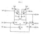
- this preferred embodiment of the latching comparator includes a first pair of n-channel field effect transistors Q2 and Q3.
- a reference input terminal or an inverting input terminal IN is connected to the gate of transistor Q2, and an inverting input voltage is supplied from terminal IN to transistor Q2.
- a non-inverting input terminal VX is connected to the gate of transistor Q3 through an n-channel field effect transistor Q8 and an inverting input node IP, and a non-inverting voltage is supplied from terminal VX to transistor Q3.
- Transistor Q8 is controlled by a clock input at a terminal EP.
- differential input voltages are fed to the latching comparator.
- inverting input terminal IN is further coupled to the gate of transistor Q3 via an n-channel field effect transistor Q9, which is controlled by another clock input at a terminal EN.
- transistor Q9 turns on and the voltage at node IP becomes the same as the inverting input voltage at terminal IN to enable the offset sampling.
- transistor Q9 turns off and transistor Q8 turns on to enter into the comparison period.
- the sources of transistors Q2 and Q3 both are connected to the drain of an n-channel field effect transistor Q1, which functions as a constant current source under the control of a bias voltage at terminal B1.
- a non-inverting output terminal DP and an inverting output terminal DN are connected to the drains of transistors Q2 and Q3 respectively.
- the latching comparator also comprises a second pair of p-channel field effect transistors Q6 and Q7.
- the sources of transistors Q6 and Q7 both are connected to a voltage supply VDD.
- the drain of transistor Q6 is connected to the drain of transistor Q2, and the drain of transistor Q7 is connected to the drain of transistor Q3.
- the gate of transistor Q6 is connected to the drain of transistor Q2 via a p-channel field effect transistor Q4, and connected to the drain of transistor Q3 via a capacitor C1.
- the gate of transistor Q7 is connected to the drain of transistor Q3 via a p-channel field effect transistor Q5, and connected to the drain of transistor Q2 via a capacitor C2.
- Transistors Q4 and Q5 are controlled by the clock input at terminal EP.
- terminals IN and IP are at the same voltage level making the input voltage difference zero.
- the outputs of DP and DN are not connected to each other.
- Terminals DP and DN are shorted to one side of each of capacitors C1 and C2 through transistors Q4 and Q5, respectively. Therefore, both outputs are clamped at certain voltages which are determined depending on the drain currents of transistors Q2,Q3 and p-channel load transistors Q6, Q7. If it is assumed that there is no offset voltage in the circuit, then the voltages at terminals DP and DN become equal to each other. And two capacitors C1 and C2 are not charged.
- the actual comparator necessarily has mismatching in the circuit, and the voltages at terminals DP and DN become different.
- This output voltage difference, delta V is stored in the capacitors C1 and C2 (FIG. 3E). For example, if there is an offset tendency that DN becomes higher than DP at zero differential input, the Q3 side of capacitor C1 stores a positive charge.
- transistors Q4, Q5 and Q9 is turned off and transistor Q8 is turned on, and the inverting input voltage at IN and the non-inverting input voltage at IP are supplied to transistors Q2 and Q3 respectively for comparing.
- the output voltage difference (delta V) generated during the offset sampling period remains in the circuit.
- the voltages at terminals DN and DP start to change, because the drain currents through transistors Q2 and Q3 begin to differ from each other due to the input voltage difference between IN and IP (VX).
- P-channel transistors Q6 and Q7 have higher gain after clamping transistors Q4 and Q5 are turned off.
- the drain current difference between load transistors Q6 and Q7 causes the voltage difference at the gates thereof via capacitors C1 and C2.
- This positive feedback loop amplifies the output voltage difference similar to the prior comparator.
- the comparator according to the present invention has a feature that the output voltages at DN and DP always move from the offset state in the proper direction during the comparison period.
- n-channel transistor Q3 conducts more and its resistance decreases, leading to increasing of the drain current which is partially supplied from pre-charged capacitor C1.
- This reduction of the voltage at DN pulls down the gate voltage of transistor Q6 through discharging and sequential reverse charging of capacitor C1. Therefore, transistor Q6 conducts more, its drain current increases and its resistance decreases to slightly raise the voltage at DP that was originally low. This rise of the voltage at DP pushes up the gate voltage of transistor Q7 through discharging and sequential reverse charging of capacitor C2.
- transistor Q7 conducts less, its drain current decreases, and the voltage at DN further decreases. This further decrease of the voltage at DN further pulls down the gate voltage of transistor Q6 through reverse charging of capacitor C1. This operating positive feedback loop finally overcomes the offset tendency and provides the proper output of the latching comparator.
- the offset cancel latching comparator according to the present invention can easily cancel the offset voltage and provide the correct comparison outputs without increasing die cost, by storing offset information in two capacitors during the offset sampling period.
Landscapes
- Manipulation Of Pulses (AREA)
- Analogue/Digital Conversion (AREA)
Applications Claiming Priority (2)
| Application Number | Priority Date | Filing Date | Title |
|---|---|---|---|
| JP294510/88 | 1988-11-24 | ||
| JP63294510A JPH02142214A (ja) | 1988-11-24 | 1988-11-24 | オフセット電圧を補償したラッチングコンパレータ |
Publications (3)
| Publication Number | Publication Date |
|---|---|
| EP0370814A2 true EP0370814A2 (de) | 1990-05-30 |
| EP0370814A3 EP0370814A3 (de) | 1991-06-12 |
| EP0370814B1 EP0370814B1 (de) | 1995-02-01 |
Family
ID=17808711
Family Applications (1)
| Application Number | Title | Priority Date | Filing Date |
|---|---|---|---|
| EP89312182A Expired - Lifetime EP0370814B1 (de) | 1988-11-24 | 1989-11-23 | Verriegelungskomparator mit Unterdrückung der Nullpunktabweichung |
Country Status (4)
| Country | Link |
|---|---|
| US (1) | US5017805A (de) |
| EP (1) | EP0370814B1 (de) |
| JP (1) | JPH02142214A (de) |
| DE (1) | DE68920964T2 (de) |
Cited By (4)
| Publication number | Priority date | Publication date | Assignee | Title |
|---|---|---|---|---|
| AU619560B2 (en) * | 1988-06-30 | 1992-01-30 | Alcatel N.V. | A schmitt trigger device |
| EP0500588A4 (en) * | 1989-10-31 | 1993-05-12 | Vlsi Technology, Inc. | High speed comparator with offset cancellation |
| EP1160983A3 (de) * | 2000-05-31 | 2009-09-23 | Nippon Telegraph and Telephone Corporation | Differentielle logische Schaltung |
| WO2022199972A1 (en) * | 2021-03-26 | 2022-09-29 | Sony Semiconductor Solutions Corporation | Pixel circuit and solid-state imaging device |
Families Citing this family (13)
| Publication number | Priority date | Publication date | Assignee | Title |
|---|---|---|---|---|
| JPH03173289A (ja) * | 1989-12-01 | 1991-07-26 | Toshiba Corp | 最大値/最小値回路 |
| JPH04211508A (ja) * | 1990-06-15 | 1992-08-03 | Toshiba Corp | 積分回路 |
| TW431067B (en) * | 1994-06-22 | 2001-04-21 | Ibm | Single source differential circuit |
| JP3416063B2 (ja) * | 1998-10-29 | 2003-06-16 | インターナショナル・ビジネス・マシーンズ・コーポレーション | センスアンプ回路 |
| JP3625194B2 (ja) | 2001-06-22 | 2005-03-02 | 松下電器産業株式会社 | オフセット補償機能付きコンパレータおよびオフセット補償機能付きd/a変換装置 |
| US6750704B1 (en) | 2003-01-09 | 2004-06-15 | Motorola, Inc. | Offset compensated differential amplifier |
| US7352307B2 (en) * | 2006-02-09 | 2008-04-01 | Atmel Corporation | Comparator chain offset reduction |
| US8072244B1 (en) * | 2010-08-31 | 2011-12-06 | National Tsing Hua University | Current sensing amplifier and method thereof |
| US8736310B2 (en) | 2010-12-17 | 2014-05-27 | Stmicroelectronics Asia Pacific Pte. Ltd. | Comparator with offset compensation and improved dynamic range |
| JP2012205043A (ja) * | 2011-03-25 | 2012-10-22 | Sony Corp | 差動増幅器及びアナログ/デジタル変換器 |
| US8570095B1 (en) * | 2012-05-11 | 2013-10-29 | Semiconductor Components Industries, Llc | Offset-compensated active load and method |
| US9650312B2 (en) | 2013-03-14 | 2017-05-16 | Lummus Technology Inc. | Integration of residue hydrocracking and hydrotreating |
| JP2021044787A (ja) * | 2019-09-13 | 2021-03-18 | キオクシア株式会社 | 半導体集積回路及び受信装置 |
Family Cites Families (6)
| Publication number | Priority date | Publication date | Assignee | Title |
|---|---|---|---|---|
| US3849673A (en) * | 1973-11-09 | 1974-11-19 | Bell Telephone Labor Inc | Compensated igfet flip-flop amplifiers |
| US4247791A (en) * | 1978-04-03 | 1981-01-27 | Rockwell International Corporation | CMOS Memory sense amplifier |
| JPS58218222A (ja) * | 1982-06-12 | 1983-12-19 | Nippon Telegr & Teleph Corp <Ntt> | 電圧比較器 |
| JPS62252597A (ja) * | 1986-04-24 | 1987-11-04 | Sony Corp | センスアンプ |
| JPS62269512A (ja) * | 1986-05-19 | 1987-11-24 | Nippon Telegr & Teleph Corp <Ntt> | 電圧比較器 |
| JPS62273694A (ja) * | 1986-05-22 | 1987-11-27 | Sony Corp | センスアンプ |
-
1988
- 1988-11-24 JP JP63294510A patent/JPH02142214A/ja active Pending
-
1989
- 1989-11-17 US US07/438,910 patent/US5017805A/en not_active Expired - Fee Related
- 1989-11-23 EP EP89312182A patent/EP0370814B1/de not_active Expired - Lifetime
- 1989-11-23 DE DE68920964T patent/DE68920964T2/de not_active Expired - Fee Related
Cited By (6)
| Publication number | Priority date | Publication date | Assignee | Title |
|---|---|---|---|---|
| AU619560B2 (en) * | 1988-06-30 | 1992-01-30 | Alcatel N.V. | A schmitt trigger device |
| EP0500588A4 (en) * | 1989-10-31 | 1993-05-12 | Vlsi Technology, Inc. | High speed comparator with offset cancellation |
| EP1160983A3 (de) * | 2000-05-31 | 2009-09-23 | Nippon Telegraph and Telephone Corporation | Differentielle logische Schaltung |
| WO2022199972A1 (en) * | 2021-03-26 | 2022-09-29 | Sony Semiconductor Solutions Corporation | Pixel circuit and solid-state imaging device |
| EP4315833A1 (de) * | 2021-03-26 | 2024-02-07 | Sony Semiconductor Solutions Corporation | Pixelschaltung und festkörperbildgebungsvorrichtung |
| US12256164B2 (en) | 2021-03-26 | 2025-03-18 | Sony Semiconductor Solutions Corporation | Pixel circuit and solid-state imaging device |
Also Published As
| Publication number | Publication date |
|---|---|
| EP0370814B1 (de) | 1995-02-01 |
| US5017805A (en) | 1991-05-21 |
| JPH02142214A (ja) | 1990-05-31 |
| DE68920964T2 (de) | 1995-09-28 |
| EP0370814A3 (de) | 1991-06-12 |
| DE68920964D1 (de) | 1995-03-16 |
Similar Documents
| Publication | Publication Date | Title |
|---|---|---|
| US5017805A (en) | Offset cancel latching comparator | |
| EP0108927B1 (de) | Schneller, nach dem Prinzip des Ladungsausgleichs arbeitender Komparator | |
| US5113090A (en) | Voltage comparator | |
| US4461965A (en) | High speed CMOS sense amplifier | |
| KR100341161B1 (ko) | 쵸퍼형전압비교기 | |
| US6046612A (en) | Self-resetting comparator circuit and method | |
| US5311085A (en) | Clocked comparator with offset-voltage compensation | |
| US5506526A (en) | Offset-compensated sample and hold arrangement and method for its operation | |
| EP0831592B1 (de) | Schneller, verbrauchsarmer Chopper Komparator mit störungsfreier Funktion bei Variation des logischen Schwellwertes der Inverter | |
| US5065045A (en) | Multistage offset-cancelled voltage comparator | |
| EP0482942A2 (de) | Dreizustands-Präzisionsausgangstreiber mit einer Spannungsklemmcharakteristik | |
| EP0015554B1 (de) | Vergleichsschaltung | |
| KR890004654B1 (ko) | 비교기회로 | |
| JP3105862B2 (ja) | 電圧比較回路 | |
| JP2857949B2 (ja) | 差動増幅器のオフセット電圧補償回路 | |
| US5410269A (en) | Sample-and-hold circuit | |
| US5165058A (en) | Voltage comparator with sample hold circuit | |
| US4323887A (en) | CMOS Analog to digital converter with selectable voltage follower buffering | |
| US20210297077A1 (en) | Sampling Circuit and Sampling Method | |
| JPH0585085B2 (de) | ||
| EP0831586A2 (de) | Variable Verzögerungsschaltung | |
| KR100273262B1 (ko) | 듀티사이클보정회로 | |
| JPH01181221A (ja) | チョッパ型コンパレータ | |
| JPS626533A (ja) | Cmosインバ−タ | |
| JPS6396800A (ja) | Cmosサンプルホ−ルド回路 |
Legal Events
| Date | Code | Title | Description |
|---|---|---|---|
| PUAI | Public reference made under article 153(3) epc to a published international application that has entered the european phase |
Free format text: ORIGINAL CODE: 0009012 |
|
| AK | Designated contracting states |
Kind code of ref document: A2 Designated state(s): DE FR GB NL |
|
| PUAL | Search report despatched |
Free format text: ORIGINAL CODE: 0009013 |
|
| AK | Designated contracting states |
Kind code of ref document: A3 Designated state(s): DE FR GB NL |
|
| 17P | Request for examination filed |
Effective date: 19910823 |
|
| 17Q | First examination report despatched |
Effective date: 19931126 |
|
| GRAA | (expected) grant |
Free format text: ORIGINAL CODE: 0009210 |
|
| RAP1 | Party data changed (applicant data changed or rights of an application transferred) |
Owner name: NIPPON MOTOROLA LTD. |
|
| AK | Designated contracting states |
Kind code of ref document: B1 Designated state(s): DE FR GB NL |
|
| REF | Corresponds to: |
Ref document number: 68920964 Country of ref document: DE Date of ref document: 19950316 |
|
| ET | Fr: translation filed | ||
| PLBE | No opposition filed within time limit |
Free format text: ORIGINAL CODE: 0009261 |
|
| STAA | Information on the status of an ep patent application or granted ep patent |
Free format text: STATUS: NO OPPOSITION FILED WITHIN TIME LIMIT |
|
| 26N | No opposition filed | ||
| PGFP | Annual fee paid to national office [announced via postgrant information from national office to epo] |
Ref country code: GB Payment date: 19970930 Year of fee payment: 9 |
|
| PGFP | Annual fee paid to national office [announced via postgrant information from national office to epo] |
Ref country code: FR Payment date: 19971015 Year of fee payment: 9 |
|
| PGFP | Annual fee paid to national office [announced via postgrant information from national office to epo] |
Ref country code: NL Payment date: 19971023 Year of fee payment: 9 |
|
| PG25 | Lapsed in a contracting state [announced via postgrant information from national office to epo] |
Ref country code: GB Free format text: LAPSE BECAUSE OF NON-PAYMENT OF DUE FEES Effective date: 19981123 |
|
| PG25 | Lapsed in a contracting state [announced via postgrant information from national office to epo] |
Ref country code: NL Free format text: LAPSE BECAUSE OF NON-PAYMENT OF DUE FEES Effective date: 19990601 |
|
| GBPC | Gb: european patent ceased through non-payment of renewal fee |
Effective date: 19981123 |
|
| PG25 | Lapsed in a contracting state [announced via postgrant information from national office to epo] |
Ref country code: FR Free format text: LAPSE BECAUSE OF NON-PAYMENT OF DUE FEES Effective date: 19990730 |
|
| NLV4 | Nl: lapsed or anulled due to non-payment of the annual fee |
Effective date: 19990601 |
|
| REG | Reference to a national code |
Ref country code: FR Ref legal event code: ST |
|
| PGFP | Annual fee paid to national office [announced via postgrant information from national office to epo] |
Ref country code: DE Payment date: 19991021 Year of fee payment: 11 |
|
| PG25 | Lapsed in a contracting state [announced via postgrant information from national office to epo] |
Ref country code: DE Free format text: LAPSE BECAUSE OF NON-PAYMENT OF DUE FEES Effective date: 20010801 |