EP0371785A2 - MOSFET latéral à modulation de conductivité - Google Patents
MOSFET latéral à modulation de conductivité Download PDFInfo
- Publication number
- EP0371785A2 EP0371785A2 EP89312428A EP89312428A EP0371785A2 EP 0371785 A2 EP0371785 A2 EP 0371785A2 EP 89312428 A EP89312428 A EP 89312428A EP 89312428 A EP89312428 A EP 89312428A EP 0371785 A2 EP0371785 A2 EP 0371785A2
- Authority
- EP
- European Patent Office
- Prior art keywords
- layer
- conductivity type
- type base
- base layer
- drain
- Prior art date
- Legal status (The legal status is an assumption and is not a legal conclusion. Google has not performed a legal analysis and makes no representation as to the accuracy of the status listed.)
- Granted
Links
Images







Classifications
-
- H—ELECTRICITY
- H10—SEMICONDUCTOR DEVICES; ELECTRIC SOLID-STATE DEVICES NOT OTHERWISE PROVIDED FOR
- H10D—INORGANIC ELECTRIC SEMICONDUCTOR DEVICES
- H10D12/00—Bipolar devices controlled by the field effect, e.g. insulated-gate bipolar transistors [IGBT]
- H10D12/411—Insulated-gate bipolar transistors [IGBT]
- H10D12/421—Insulated-gate bipolar transistors [IGBT] on insulating layers or insulating substrates, e.g. thin-film IGBTs
-
- H—ELECTRICITY
- H10—SEMICONDUCTOR DEVICES; ELECTRIC SOLID-STATE DEVICES NOT OTHERWISE PROVIDED FOR
- H10D—INORGANIC ELECTRIC SEMICONDUCTOR DEVICES
- H10D12/00—Bipolar devices controlled by the field effect, e.g. insulated-gate bipolar transistors [IGBT]
- H10D12/411—Insulated-gate bipolar transistors [IGBT]
-
- H—ELECTRICITY
- H10—SEMICONDUCTOR DEVICES; ELECTRIC SOLID-STATE DEVICES NOT OTHERWISE PROVIDED FOR
- H10D—INORGANIC ELECTRIC SEMICONDUCTOR DEVICES
- H10D62/00—Semiconductor bodies, or regions thereof, of devices having potential barriers
- H10D62/10—Shapes, relative sizes or dispositions of the regions of the semiconductor bodies; Shapes of the semiconductor bodies
- H10D62/124—Shapes, relative sizes or dispositions of the regions of semiconductor bodies or of junctions between the regions
- H10D62/126—Top-view geometrical layouts of the regions or the junctions
- H10D62/127—Top-view geometrical layouts of the regions or the junctions of cellular field-effect devices, e.g. multicellular DMOS transistors or IGBTs
-
- H—ELECTRICITY
- H10—SEMICONDUCTOR DEVICES; ELECTRIC SOLID-STATE DEVICES NOT OTHERWISE PROVIDED FOR
- H10D—INORGANIC ELECTRIC SEMICONDUCTOR DEVICES
- H10D62/00—Semiconductor bodies, or regions thereof, of devices having potential barriers
- H10D62/10—Shapes, relative sizes or dispositions of the regions of the semiconductor bodies; Shapes of the semiconductor bodies
- H10D62/13—Semiconductor regions connected to electrodes carrying current to be rectified, amplified or switched, e.g. source or drain regions
- H10D62/141—Anode or cathode regions of thyristors; Collector or emitter regions of gated bipolar-mode devices, e.g. of IGBTs
- H10D62/142—Anode regions of thyristors or collector regions of gated bipolar-mode devices
Definitions
- a lateral conductivity modulated MOSFET which utilizes conductivity modulation caused by electrons and holes accumulated in a drift layer is disclosed in M. Darwish et al. "Lateral Resurfed COMFET.” Electronics Letters . 7th June 1984, Vol. 20 No. 12, pp. 519-520.
- carriers accumulated in an n-type base layer must be swiftly eliminated, so as to increase the switching speed at the time of turn-off operation. If the electrons do not swiftly move from the n-type base layer to the drain layer, a pnp transistor constituted by a p-type drain layer, an n-type base layer and p-type base layer operates.
- the holes injected from the p-type drain layer to the n-type base layer are crowded out of the n-type base layer and are stored in the wafer.
- electrons are injected from the n-type base layer into the wafer.
- these electrodes are easily expelled from the wafer into the cathode layer, which is at the same potential level as that of the drain layer.
- the ON-state voltage is low, and the turn-off characteristic is satisfactory.
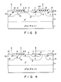
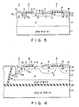
- Oxide film 19 is formed on the inner wall of the groove, and polycrystalline silicon film 20 is formed in the groove in such a manner as to fill the groove.
- This type of wafer which has two parts isolated by a dielectric, may be also formed by burying single-crystal silicon into a polycrystalline silicon substrate.
Landscapes
- Insulated Gate Type Field-Effect Transistor (AREA)
- Bipolar Transistors (AREA)
Applications Claiming Priority (4)
| Application Number | Priority Date | Filing Date | Title |
|---|---|---|---|
| JP301718/88 | 1988-11-29 | ||
| JP30171888 | 1988-11-29 | ||
| JP123601/89 | 1989-05-17 | ||
| JP1123601A JP2724204B2 (ja) | 1988-11-29 | 1989-05-17 | 導電変調型mosfet |
Publications (3)
| Publication Number | Publication Date |
|---|---|
| EP0371785A2 true EP0371785A2 (fr) | 1990-06-06 |
| EP0371785A3 EP0371785A3 (fr) | 1991-09-18 |
| EP0371785B1 EP0371785B1 (fr) | 1996-05-01 |
Family
ID=26460481
Family Applications (1)
| Application Number | Title | Priority Date | Filing Date |
|---|---|---|---|
| EP89312428A Expired - Lifetime EP0371785B1 (fr) | 1988-11-29 | 1989-11-29 | MOSFET latéral à modulation de conductivité |
Country Status (3)
| Country | Link |
|---|---|
| US (1) | US5068700A (fr) |
| EP (1) | EP0371785B1 (fr) |
| DE (1) | DE68926384T2 (fr) |
Cited By (6)
| Publication number | Priority date | Publication date | Assignee | Title |
|---|---|---|---|---|
| EP0594111A1 (fr) * | 1992-10-19 | 1994-04-27 | Fuji Electric Co., Ltd. | Transistor MIS haute-tension et dispositif semi-conducteur |
| EP0526939B1 (fr) * | 1991-08-07 | 1996-05-01 | Koninklijke Philips Electronics N.V. | Transistor semi-conducteur bipolaire latéral à grille isolée |
| DE19507169C1 (de) * | 1995-03-01 | 1996-06-13 | Siemens Ag | Integrierte Schaltungsanordnung mit mindestens einem IGBT |
| DE19630740B4 (de) * | 1996-03-20 | 2005-06-02 | Korea Electronics Co., Ltd., Kumi | Bipolarer Transistor mit Kurzschlußanode und seitlich angeordneter isolierter Gate-Elektrode |
| US7602025B2 (en) * | 2006-12-08 | 2009-10-13 | Panasonic Corporation | High voltage semiconductor device and method of manufacture thereof |
| WO2021128435A1 (fr) * | 2019-12-28 | 2021-07-01 | 汪克明 | Nouveaux principes et technologie pour l'électronique à semi-conducteurs, et dispositif |
Families Citing this family (35)
| Publication number | Priority date | Publication date | Assignee | Title |
|---|---|---|---|---|
| US5273917A (en) * | 1989-08-19 | 1993-12-28 | Fuji Electric Co., Ltd. | Method for manufacturing a conductivity modulation MOSFET |
| JP2609753B2 (ja) * | 1990-10-17 | 1997-05-14 | 株式会社東芝 | 半導体装置 |
| US5258636A (en) * | 1991-12-12 | 1993-11-02 | Power Integrations, Inc. | Narrow radius tips for high voltage semiconductor devices with interdigitated source and drain electrodes |
| US5548150A (en) * | 1993-03-10 | 1996-08-20 | Kabushiki Kaisha Toshiba | Field effect transistor |
| US5382536A (en) * | 1993-03-15 | 1995-01-17 | Texas Instruments Incorporated | Method of fabricating lateral DMOS structure |
| US5369045A (en) * | 1993-07-01 | 1994-11-29 | Texas Instruments Incorporated | Method for forming a self-aligned lateral DMOS transistor |
| US5710451A (en) * | 1996-04-10 | 1998-01-20 | Philips Electronics North America Corporation | High-voltage lateral MOSFET SOI device having a semiconductor linkup region |
| SE513284C2 (sv) * | 1996-07-26 | 2000-08-14 | Ericsson Telefon Ab L M | Halvledarkomponent med linjär ström-till-spänningskarasterik |
| JP3527034B2 (ja) * | 1996-09-20 | 2004-05-17 | 株式会社半導体エネルギー研究所 | 半導体装置 |
| US6084277A (en) * | 1999-02-18 | 2000-07-04 | Power Integrations, Inc. | Lateral power MOSFET with improved gate design |
| US6593594B1 (en) * | 1999-12-21 | 2003-07-15 | Koninklijke Philips Electonics N.V. | Silicon carbide n-channel power LMOSFET |
| JP4357127B2 (ja) | 2000-03-03 | 2009-11-04 | 株式会社東芝 | 半導体装置 |
| JP2002094063A (ja) | 2000-09-11 | 2002-03-29 | Toshiba Corp | 半導体装置 |
| US6509220B2 (en) | 2000-11-27 | 2003-01-21 | Power Integrations, Inc. | Method of fabricating a high-voltage transistor |
| US6768171B2 (en) | 2000-11-27 | 2004-07-27 | Power Integrations, Inc. | High-voltage transistor with JFET conduction channels |
| US6424007B1 (en) | 2001-01-24 | 2002-07-23 | Power Integrations, Inc. | High-voltage transistor with buried conduction layer |
| JP3647802B2 (ja) | 2001-01-25 | 2005-05-18 | 株式会社東芝 | 横型半導体装置 |
| US6573558B2 (en) * | 2001-09-07 | 2003-06-03 | Power Integrations, Inc. | High-voltage vertical transistor with a multi-layered extended drain structure |
| US6555873B2 (en) * | 2001-09-07 | 2003-04-29 | Power Integrations, Inc. | High-voltage lateral transistor with a multi-layered extended drain structure |
| US6635544B2 (en) | 2001-09-07 | 2003-10-21 | Power Intergrations, Inc. | Method of fabricating a high-voltage transistor with a multi-layered extended drain structure |
| US7786533B2 (en) * | 2001-09-07 | 2010-08-31 | Power Integrations, Inc. | High-voltage vertical transistor with edge termination structure |
| US7221011B2 (en) * | 2001-09-07 | 2007-05-22 | Power Integrations, Inc. | High-voltage vertical transistor with a multi-gradient drain doping profile |
| US20060163658A1 (en) | 2005-01-21 | 2006-07-27 | Anderson Samuel J | Monolithic MOSFET and schottky diode for mobile phone boost converter |
| JP4730529B2 (ja) * | 2005-07-13 | 2011-07-20 | サンケン電気株式会社 | 電界効果トランジスタ |
| US7859037B2 (en) * | 2007-02-16 | 2010-12-28 | Power Integrations, Inc. | Checkerboarded high-voltage vertical transistor layout |
| US7595523B2 (en) | 2007-02-16 | 2009-09-29 | Power Integrations, Inc. | Gate pullback at ends of high-voltage vertical transistor structure |
| US7557406B2 (en) | 2007-02-16 | 2009-07-07 | Power Integrations, Inc. | Segmented pillar layout for a high-voltage vertical transistor |
| US8653583B2 (en) | 2007-02-16 | 2014-02-18 | Power Integrations, Inc. | Sensing FET integrated with a high-voltage transistor |
| US7468536B2 (en) | 2007-02-16 | 2008-12-23 | Power Integrations, Inc. | Gate metal routing for transistor with checkerboarded layout |
| KR102016986B1 (ko) * | 2013-01-25 | 2019-09-02 | 삼성전자주식회사 | 엘디모스 트랜지스터 기반의 다이오드 및 이를 포함하는 정전기 방전 보호 회로 |
| US9660053B2 (en) | 2013-07-12 | 2017-05-23 | Power Integrations, Inc. | High-voltage field-effect transistor having multiple implanted layers |
| CN105556647B (zh) * | 2013-07-19 | 2017-06-13 | 日产自动车株式会社 | 半导体装置及其制造方法 |
| US9997599B2 (en) * | 2013-10-07 | 2018-06-12 | Purdue Research Foundation | MOS-based power semiconductor device having increased current carrying area and method of fabricating same |
| US9543396B2 (en) | 2013-12-13 | 2017-01-10 | Power Integrations, Inc. | Vertical transistor device structure with cylindrically-shaped regions |
| US10325988B2 (en) | 2013-12-13 | 2019-06-18 | Power Integrations, Inc. | Vertical transistor device structure with cylindrically-shaped field plates |
Family Cites Families (20)
| Publication number | Priority date | Publication date | Assignee | Title |
|---|---|---|---|---|
| US4300150A (en) * | 1980-06-16 | 1981-11-10 | North American Philips Corporation | Lateral double-diffused MOS transistor device |
| JPS57206073A (en) * | 1981-06-12 | 1982-12-17 | Hitachi Ltd | Mis semiconductor device |
| US4782379A (en) * | 1981-11-23 | 1988-11-01 | General Electric Company | Semiconductor device having rapid removal of majority carriers from an active base region thereof at device turn-off and method of fabricating this device |
| US4742380A (en) * | 1982-02-09 | 1988-05-03 | American Telephone And Telegraph Company, At&T Bell Laboratories | Switch utilizing solid-state relay |
| JPH0612828B2 (ja) * | 1983-06-30 | 1994-02-16 | 株式会社東芝 | 半導体装置 |
| JPS60196974A (ja) * | 1984-03-19 | 1985-10-05 | Toshiba Corp | 導電変調型mosfet |
| US4672407A (en) * | 1984-05-30 | 1987-06-09 | Kabushiki Kaisha Toshiba | Conductivity modulated MOSFET |
| US4593458A (en) * | 1984-11-02 | 1986-06-10 | General Electric Company | Fabrication of integrated circuit with complementary, dielectrically-isolated, high voltage semiconductor devices |
| JPS61171165A (ja) * | 1985-01-25 | 1986-08-01 | Nissan Motor Co Ltd | Mosトランジスタ |
| JPS6239069A (ja) * | 1985-08-13 | 1987-02-20 | Mitsubishi Electric Corp | 電界効果型半導体装置 |
| DE3628857A1 (de) * | 1985-08-27 | 1987-03-12 | Mitsubishi Electric Corp | Halbleitereinrichtung |
| JPS6258683A (ja) * | 1985-09-06 | 1987-03-14 | Matsushita Electric Ind Co Ltd | 電界効果トランジスタ |
| CA1252225A (fr) * | 1985-11-27 | 1989-04-04 | Sel Colak | Transistor a grille isolee lateral a regions d'anode et de grille couplees |
| US4779123A (en) * | 1985-12-13 | 1988-10-18 | Siliconix Incorporated | Insulated gate transistor array |
| JPS63173365A (ja) * | 1986-11-26 | 1988-07-16 | ゼネラル・エレクトリック・カンパニイ | ラテラル形絶縁ゲート半導体装置とその製法 |
| US4857983A (en) * | 1987-05-19 | 1989-08-15 | General Electric Company | Monolithically integrated semiconductor device having bidirectional conducting capability and method of fabrication |
| US4811065A (en) * | 1987-06-11 | 1989-03-07 | Siliconix Incorporated | Power DMOS transistor with high speed body diode |
| US4939566A (en) * | 1987-10-30 | 1990-07-03 | North American Philips Corporation | Semiconductor switch with parallel DMOS and IGT |
| US4861731A (en) * | 1988-02-02 | 1989-08-29 | General Motors Corporation | Method of fabricating a lateral dual gate thyristor |
| US4873563A (en) * | 1988-05-02 | 1989-10-10 | Synectics, Inc. | Solid state monolithic switching device |
-
1989
- 1989-11-29 EP EP89312428A patent/EP0371785B1/fr not_active Expired - Lifetime
- 1989-11-29 DE DE68926384T patent/DE68926384T2/de not_active Expired - Fee Related
-
1990
- 1990-11-29 US US07/622,351 patent/US5068700A/en not_active Expired - Lifetime
Cited By (8)
| Publication number | Priority date | Publication date | Assignee | Title |
|---|---|---|---|---|
| EP0526939B1 (fr) * | 1991-08-07 | 1996-05-01 | Koninklijke Philips Electronics N.V. | Transistor semi-conducteur bipolaire latéral à grille isolée |
| EP0594111A1 (fr) * | 1992-10-19 | 1994-04-27 | Fuji Electric Co., Ltd. | Transistor MIS haute-tension et dispositif semi-conducteur |
| US5436486A (en) * | 1992-10-19 | 1995-07-25 | Fuji Electric Co., Ltd. | High voltage MIS transistor and semiconductor device |
| DE19507169C1 (de) * | 1995-03-01 | 1996-06-13 | Siemens Ag | Integrierte Schaltungsanordnung mit mindestens einem IGBT |
| US5760424A (en) * | 1995-03-01 | 1998-06-02 | Siemens Aktiengesellschaft | Integrated circuit arrangement having at least one IGBT |
| DE19630740B4 (de) * | 1996-03-20 | 2005-06-02 | Korea Electronics Co., Ltd., Kumi | Bipolarer Transistor mit Kurzschlußanode und seitlich angeordneter isolierter Gate-Elektrode |
| US7602025B2 (en) * | 2006-12-08 | 2009-10-13 | Panasonic Corporation | High voltage semiconductor device and method of manufacture thereof |
| WO2021128435A1 (fr) * | 2019-12-28 | 2021-07-01 | 汪克明 | Nouveaux principes et technologie pour l'électronique à semi-conducteurs, et dispositif |
Also Published As
| Publication number | Publication date |
|---|---|
| DE68926384D1 (de) | 1996-06-05 |
| EP0371785B1 (fr) | 1996-05-01 |
| DE68926384T2 (de) | 1996-10-10 |
| EP0371785A3 (fr) | 1991-09-18 |
| US5068700A (en) | 1991-11-26 |
Similar Documents
| Publication | Publication Date | Title |
|---|---|---|
| US5068700A (en) | Lateral conductivity modulated mosfet | |
| US5089864A (en) | Insulated gate type semiconductor device | |
| US5572048A (en) | Voltage-driven type semiconductor device | |
| US6737705B2 (en) | Insulated gate semiconductor device | |
| JP3325736B2 (ja) | 絶縁ゲート型半導体装置 | |
| US4969028A (en) | Gate enhanced rectifier | |
| US6091107A (en) | Semiconductor devices | |
| US5070377A (en) | Semiconductor device and method of manufacturing the same | |
| US4717940A (en) | MIS controlled gate turn-off thyristor | |
| EP0697739B1 (fr) | Transistor bipolaire à grille isolée | |
| US4969027A (en) | Power bipolar transistor device with integral antisaturation diode | |
| US20020053717A1 (en) | Semiconductor apparatus | |
| US5910664A (en) | Emitter-switched transistor structures | |
| JP2809253B2 (ja) | 注入制御型ショットキーバリア整流素子 | |
| JPH0575110A (ja) | 半導体装置 | |
| EP0228107A2 (fr) | Transistors latéraux à grille isolée commutant rapidement | |
| JPH0716009B2 (ja) | 横型絶縁ゲートバイポーラトランジスタ | |
| US5079607A (en) | Mos type semiconductor device | |
| KR100278526B1 (ko) | 반도체 소자 | |
| JPH07169868A (ja) | 少なくとも1個のバイポーラ・パワーデバイスを有する回路パターン及びその作動方法 | |
| EP0913872A1 (fr) | Transistor bipolaire à grille isolée | |
| US5757034A (en) | Emitter switched thyristor | |
| US5587595A (en) | Lateral field-effect-controlled semiconductor device on insulating substrate | |
| US5621229A (en) | Semiconductor device and control method | |
| US5808345A (en) | High speed IGBT |
Legal Events
| Date | Code | Title | Description |
|---|---|---|---|
| PUAI | Public reference made under article 153(3) epc to a published international application that has entered the european phase |
Free format text: ORIGINAL CODE: 0009012 |
|
| 17P | Request for examination filed |
Effective date: 19891214 |
|
| AK | Designated contracting states |
Kind code of ref document: A2 Designated state(s): DE IT |
|
| PUAL | Search report despatched |
Free format text: ORIGINAL CODE: 0009013 |
|
| AK | Designated contracting states |
Kind code of ref document: A3 Designated state(s): DE IT |
|
| 16A | New documents despatched to applicant after publication of the search report | ||
| 17Q | First examination report despatched |
Effective date: 19930915 |
|
| RBV | Designated contracting states (corrected) |
Designated state(s): DE |
|
| GRAA | (expected) grant |
Free format text: ORIGINAL CODE: 0009210 |
|
| AK | Designated contracting states |
Kind code of ref document: B1 Designated state(s): DE |
|
| REF | Corresponds to: |
Ref document number: 68926384 Country of ref document: DE Date of ref document: 19960605 |
|
| GRAH | Despatch of communication of intention to grant a patent |
Free format text: ORIGINAL CODE: EPIDOS IGRA |
|
| PLBE | No opposition filed within time limit |
Free format text: ORIGINAL CODE: 0009261 |
|
| STAA | Information on the status of an ep patent application or granted ep patent |
Free format text: STATUS: NO OPPOSITION FILED WITHIN TIME LIMIT |
|
| 26N | No opposition filed | ||
| PGFP | Annual fee paid to national office [announced via postgrant information from national office to epo] |
Ref country code: DE Payment date: 20051124 Year of fee payment: 17 |
|
| PG25 | Lapsed in a contracting state [announced via postgrant information from national office to epo] |
Ref country code: DE Free format text: LAPSE BECAUSE OF NON-PAYMENT OF DUE FEES Effective date: 20070601 |