EP0373400A2 - Isolierte Leitung und Verfahren zu ihrer Herstellung - Google Patents
Isolierte Leitung und Verfahren zu ihrer Herstellung Download PDFInfo
- Publication number
- EP0373400A2 EP0373400A2 EP89121668A EP89121668A EP0373400A2 EP 0373400 A2 EP0373400 A2 EP 0373400A2 EP 89121668 A EP89121668 A EP 89121668A EP 89121668 A EP89121668 A EP 89121668A EP 0373400 A2 EP0373400 A2 EP 0373400A2
- Authority
- EP
- European Patent Office
- Prior art keywords
- microspheres
- insulated conductor
- resin composition
- coating
- curable resin
- Prior art date
- Legal status (The legal status is an assumption and is not a legal conclusion. Google has not performed a legal analysis and makes no representation as to the accuracy of the status listed.)
- Granted
Links
Images

Classifications
-
- H—ELECTRICITY
- H01—ELECTRIC ELEMENTS
- H01B—CABLES; CONDUCTORS; INSULATORS; SELECTION OF MATERIALS FOR THEIR CONDUCTIVE, INSULATING OR DIELECTRIC PROPERTIES
- H01B7/00—Insulated conductors or cables characterised by their form
- H01B7/02—Disposition of insulation
-
- H—ELECTRICITY
- H01—ELECTRIC ELEMENTS
- H01B—CABLES; CONDUCTORS; INSULATORS; SELECTION OF MATERIALS FOR THEIR CONDUCTIVE, INSULATING OR DIELECTRIC PROPERTIES
- H01B3/00—Insulators or insulating bodies characterised by the insulating materials; Selection of materials for their insulating or dielectric properties
- H01B3/18—Insulators or insulating bodies characterised by the insulating materials; Selection of materials for their insulating or dielectric properties mainly consisting of organic substances
- H01B3/30—Insulators or insulating bodies characterised by the insulating materials; Selection of materials for their insulating or dielectric properties mainly consisting of organic substances plastics; resins; waxes
- H01B3/44—Insulators or insulating bodies characterised by the insulating materials; Selection of materials for their insulating or dielectric properties mainly consisting of organic substances plastics; resins; waxes vinyl resins; acrylic resins
-
- C—CHEMISTRY; METALLURGY
- C08—ORGANIC MACROMOLECULAR COMPOUNDS; THEIR PREPARATION OR CHEMICAL WORKING-UP; COMPOSITIONS BASED THEREON
- C08J—WORKING-UP; GENERAL PROCESSES OF COMPOUNDING; AFTER-TREATMENT NOT COVERED BY SUBCLASSES C08B, C08C, C08F, C08G or C08H
- C08J9/00—Working-up of macromolecular substances to porous or cellular articles or materials; After-treatment thereof
- C08J9/32—Working-up of macromolecular substances to porous or cellular articles or materials; After-treatment thereof from compositions containing microballoons, e.g. syntactic foams
-
- H—ELECTRICITY
- H01—ELECTRIC ELEMENTS
- H01B—CABLES; CONDUCTORS; INSULATORS; SELECTION OF MATERIALS FOR THEIR CONDUCTIVE, INSULATING OR DIELECTRIC PROPERTIES
- H01B3/00—Insulators or insulating bodies characterised by the insulating materials; Selection of materials for their insulating or dielectric properties
- H01B3/18—Insulators or insulating bodies characterised by the insulating materials; Selection of materials for their insulating or dielectric properties mainly consisting of organic substances
- H01B3/30—Insulators or insulating bodies characterised by the insulating materials; Selection of materials for their insulating or dielectric properties mainly consisting of organic substances plastics; resins; waxes
- H01B3/46—Insulators or insulating bodies characterised by the insulating materials; Selection of materials for their insulating or dielectric properties mainly consisting of organic substances plastics; resins; waxes silicones
-
- Y—GENERAL TAGGING OF NEW TECHNOLOGICAL DEVELOPMENTS; GENERAL TAGGING OF CROSS-SECTIONAL TECHNOLOGIES SPANNING OVER SEVERAL SECTIONS OF THE IPC; TECHNICAL SUBJECTS COVERED BY FORMER USPC CROSS-REFERENCE ART COLLECTIONS [XRACs] AND DIGESTS
- Y10—TECHNICAL SUBJECTS COVERED BY FORMER USPC
- Y10T—TECHNICAL SUBJECTS COVERED BY FORMER US CLASSIFICATION
- Y10T428/00—Stock material or miscellaneous articles
- Y10T428/249921—Web or sheet containing structurally defined element or component
- Y10T428/249953—Composite having voids in a component [e.g., porous, cellular, etc.]
- Y10T428/249971—Preformed hollow element-containing
- Y10T428/249972—Resin or rubber element
-
- Y—GENERAL TAGGING OF NEW TECHNOLOGICAL DEVELOPMENTS; GENERAL TAGGING OF CROSS-SECTIONAL TECHNOLOGIES SPANNING OVER SEVERAL SECTIONS OF THE IPC; TECHNICAL SUBJECTS COVERED BY FORMER USPC CROSS-REFERENCE ART COLLECTIONS [XRACs] AND DIGESTS
- Y10—TECHNICAL SUBJECTS COVERED BY FORMER USPC
- Y10T—TECHNICAL SUBJECTS COVERED BY FORMER US CLASSIFICATION
- Y10T428/00—Stock material or miscellaneous articles
- Y10T428/249921—Web or sheet containing structurally defined element or component
- Y10T428/249953—Composite having voids in a component [e.g., porous, cellular, etc.]
- Y10T428/249971—Preformed hollow element-containing
- Y10T428/249974—Metal- or silicon-containing element
-
- Y—GENERAL TAGGING OF NEW TECHNOLOGICAL DEVELOPMENTS; GENERAL TAGGING OF CROSS-SECTIONAL TECHNOLOGIES SPANNING OVER SEVERAL SECTIONS OF THE IPC; TECHNICAL SUBJECTS COVERED BY FORMER USPC CROSS-REFERENCE ART COLLECTIONS [XRACs] AND DIGESTS
- Y10—TECHNICAL SUBJECTS COVERED BY FORMER USPC
- Y10T—TECHNICAL SUBJECTS COVERED BY FORMER US CLASSIFICATION
- Y10T428/00—Stock material or miscellaneous articles
- Y10T428/25—Web or sheet containing structurally defined element or component and including a second component containing structurally defined particles
- Y10T428/254—Polymeric or resinous material
Definitions
- the present invention relates to an insulated conductor of small diameter and having a low dielectric constant and a method of producing the same.
- a foaming and extruding technique as described in Japanese Patent Post-examination Publication No. 57-30253 is known as one prior art technique for forming a thin-film insulating layer on a conductor.
- an insulating layer having a low dielectric constant can be produced with a large void ratio obtained by foaming a polyolefin resin by use of any one of several chemical foaming agents, such as azodicarbonamide and the like, inert gases, such as nitrogen gas, argon gas and the like, and gas-like or liquid-like hydrocarbons or fluorocarbons.
- Japanese Patent Unexamination Publication (OPI) Nos. 56-43564 and 57-39006 have proposed a method for fusing and extruding microspheres or foam microspheres formed of an inorganic material, such as glass, alumina or the like, having particle diameter of several ⁇ m to several mm and coated with a thermoplastic resin, and a method for producing an insulated conductor comprising the steps of: dissolving a thermoplastic resin, such as polyethylene, polyvinyl chloride or the like, in a solvent such as xylene or the like; applying the resulting solution on a conductor; and drying the resulting solution.
- a thermoplastic resin such as polyethylene, polyvinyl chloride or the like
- the method as described in the Japanese Patent Post-examination Publication No. 57-30253 has a disadvantage in that the thickness of the coating layer is limited to not less than 200 ⁇ m, because fusion of a polyolefin resin, foaming thereof and application thereof onto a conductor are carried out simultaneously by a screw extruder to thereby make it difficult to attain a high foaming rate in the thin-film insulating layer. Furthermore, the method has a disadvantage in that the foaming rate cannot be controlled easily.
- thermoplastic resin covering the surface of each microsphere is fused, applied on the conductor and then cooled to join the microsphere. Accordingly, as the thermoplastic resin layer is thinned for the purpose of attaining a high void ratio, the mechanical strength, particularly the elongation rate, of the insulating layer formed on the conductor are lowered remarkably. As the thermoplastic resin layer of the microsphere is thickened to maintain the mechanical strength of the insulating layer, the void ratio decreases so that the dielectric constant of the insulated conductor increases.
- the material used for the microsphere is limited to inorganic materials, such as glass, alumina and the like. And, since each of the materials for the microsphere has such a high intrinsic dielectric constant, a cable with a low dielectric constant and low loss cannot be produced.
- the latter method for producing an insulated conductor comprises the steps of: dissolving a thermoplastic resin, such as polyethylene, polyvinyl chloride or the like, and inorganic-material microspheres in a solvent such as xylene or the like; applying the resulting solution on a conductor; and drying the resulting solution, with heating being required for drying, similar to the former method. Since the material used for the microsphere is also limited, it is, like the former method, difficult to produce a cable with a low dielectric constant and low loss. Further, the manufacturing speed is very slow, because the solvent in the applied liquid-like composition is evaporates.
- the present invention is directed to an insulated conductor formed by coating a conductor with an insulating layer, the insulating layer being composed of a mixture of an energy irradiation curable resin composition and microspheres.
- the insulated conductor is excellent in that low capacitance can be obtained in spite of thin-film coating, variations in capacitance due to the manufacturing process are less, the coating layer is smooth, and high-speed manufacture is possible.
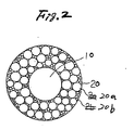
- the microspheres used herein may be all of equal mean diameter or may be of at least two different mean diameters.
- the aforementioned insulated conductor is embodied in the present invention by a method of producing an insulated conductor comprising the steps of: mixing microspheres in an energy irradiation curable resin composition to prepare a coating resin composition; applying the coating resin composition on the outer surface of a conductor; and hardening the coating resin composition through energy irradiation to thereby form a coating layer.
- the energy irradiation curable resin composition used in the present invention is preferably an ultraviolet-ray curable resin composition.
- the coating resin composition used in the present invention is an energy irradiation curable resin composition or a mixture of an energy irradiation curable resin and microspheres contained therein.
- the microspheres used in the present invention each contain air or another gas, such as nitrogen gas, argon gas, isobutane gas or the like; and has a shell portion made of any suitable material selected from thermo-plastic resins, such as vinylidene chloride-acrylonitrile copolymer, polyethylene, fluororesin and the like; thermocurable resins, such as epoxy resin, phenol resin, urea resin and the like; and inorganic materials, such as silica, alumina, carbon, zirconia, modifications thereof, and the like.
- thermo-plastic resins such as vinylidene chloride-acrylonitrile copolymer, polyethylene, fluororesin and the like
- thermocurable resins such as epoxy resin, phenol resin, urea resin and the like
- inorganic materials such as silica, alumina, carbon, zirconia, modifications thereof, and the like.
- the surfaces of the microspheres may be treated with a silane coupling agent or the like.
- Vinylidene chloride-acrylonitrile copolymer or the like is preferably employed, compared with silica, from the point of view of lowering its dielectric constant.
- the microspheres preferably have mean diameters within a range of from 1 to 100 ⁇ m ⁇ and shell thicknesses no greater than 0.5 ⁇ m to attain a coating layer with a low dielectric constant and a thickness no greater than 200 ⁇ m. This is because the void ratio is increased by mixing the microspheres without lowering the smoothness of the coating layer.
- At least two kinds of microspheres which have differing mean diameter can be selected from microspheres having mean diameters within a range of 1 to 100 ⁇ m ⁇ and a shell thickness of not larger than 0.5 ⁇ m. This makes it possible to increase the void ratio by mixing the microspheres without decreasing the smoothness of the coating layer.
- the microspheres which differ in mean diameter may be made of the same or different materials. It is however preferable that the dielectric constant of the material for the smaller mean diameter microspheres not be higher than the dielectric constant of the material for the larger mean diameter microspheres.
- Examples of the energy irradiation curable resin composition related to the present invention include a thermocurable resin, an ultraviolet-ray curable resin, and an electron beam curable resin. From the standpoint of forming a coating quickly, an ultraviolet-ray curable resin is preferred.
- Examples of the energy irradiation curable resins used herein include silicone resin, epoxy resin, urethane resin, polyester resin, epoxy acrylate, urethane acrylate, fluoracrylate, silicone acrylate, polyester acrylate, and the like.
- the dielectric constant of the energy irradiation curable resin composition be low. Accordingly, the dielectric constant of the energy irradiation curable resin should not be larger than 4.0, preferably not larger than 3.0.
- the resin be selected from silicone resin, fluoracrylate, silicone acrylate and the like.
- additives such as foaming agents, oxidation inhibitors, light stabilizers, resin coupling agents, surface treating agents, particle dispersing agents, and the like, when added to the coating resin of this type insulating conductor, are effective for improving the low capacitance in the coating resin, while also improving the stability, mechanical characteristics, functional characteristics and the like.
- the microspheres and the energy irradiation curable resin are mixed in a volumetric proportion not less than 1 : 1. This is because when the volumetric proportion is less than 1, the void ratio of the coating resin produced by mixing the microspheres is less than 40% thereby making it impossible to obtain a coating layer of low capacitance and low dielectric constant.
- the preferred range of the diameter of the microspheres used in the present invention is as follows.
- the two kinds preferably satisfy the relation r2/r1 ⁇ 0.224 in which r1 represents the mean diameter of one kind of microsphere, 1, and r2 represents the mean diameter of the other kind of microsphere, 2.
- the range of the viscosity of the coating resin composition is from 100 to 100,000 cps.
- the range of the viscosity is preferably from 1,000 to 10,000 cps.
- ultraviolet-ray curable resin is suitable to prepare the coating resin composition of 1,000 to 10,000 cps, because the viscosity thereof can be selected freely.
- the coating thickness is not limited specifically, the preferred thickness should not be larger than 500 ⁇ m in order to harden the energy radiation setting resin sufficiently.
- the conductor of the present invention is not limited specifically.
- a known electrical conductor for example, copper, aluminum, alloys thereof, or conductors plated with the above mentioned metals, or the like, can be used.
- a coating resin composition comprising a mixture of microspheres of the same mean diameter and an energy irradiation setting resin or a mixture of at least two kinds of microspheres different in mean diameter and an energy irradiation curable resin is applied to the outer surface of the conductor 4 fed out from a supply means designated by the numeral 3 in Fig. 3.
- the coating resin composition thus applied is subjected to irradiation of energy, such as heat, ultraviolet rays, an electron beam, or the like, supplied from a resin hardening means 6, so that the coating resin composition is hardened to form a coating on the conductor 4 to thereby prepare an insulated conductor 7 according to the present invention.
- the reference numeral 8 designates a takeup means.
- the resin coating device 5 is the means by which the coating resin composition containing microspheres and having a relatively high viscosity can be uniformly applied.
- Known techniques such as a technique of coating by use of a pressure die, a technique of dipping by use of an open die, and the like, can be used as the resin coating device 5.
- the void ratio V is measured by a density method and calculated by the following equation (1). ( ⁇ 0 - ⁇ ) / ⁇ 0 x 100 (%) (1) ⁇ 0 represents the density of base resin, and ⁇ represents the density of microsphere-containing resin.
- the dielectric constant, ⁇ , of a microsphere-containing resin composition is determined by the dielectric constant ⁇ 1 of the base resin, the dielectric constant ⁇ 2 of a gas contained in the microsphere, and the void ratio V produced by mixing the microspheres in the base resin, and that the dielectric constant ⁇ is represented by the following equation (2), when shell thickness of the microsphere is very thin and the dielectric constant of the shell material is negligible.
- desired voids can be formed stably in the coating layer by selecting the material for forming the microspheres, the void ratio thereof, the content of the microspheres in the resin composition, and the material for the resin composition, respectively, and it is therefore possible to form an insulating layer having a desired dielectric constant.
- the dielectric constant ⁇ 1 of the base resin must be selected so as to increase the void ratio to a value larger than 40% because the lowest dielectric constant of all resin, which fluorocarbon resin has, is 2.
- the base resin is required to be subjected to a high temperature for hardening, there is a risk that the gas contained in the microspheres may expand and contract and that the microspheres may become deformed with the result that the void ratio cannot be maintained.
- the microspheres which help give the resin a low-dielectric constant can be used because it is not necessary to heat the ultraviolet-ray curable resin to harden it.
- an added way of attaining a very low dielectric constant in the resin is by selecting a resin with an intrinsically low dielectric constant as the energy irradiation curable resin.
- the microspheres have a mean diameter within a range of about 1 to about 100 ⁇ m and a shell thickness not larger than 0.5 ⁇ m, voids can be formed securely even if the coating is made of a thin film. Accordingly, it is possible to produce an insulated conductor capable of high-speed transmission in which the capacitance of the insulating layer is not larger than 1.60, which would not have been possible in the prior art products, even where the thickness of the insulating layer is not larger than 200 ⁇ m.
- an energy irradiation curable resin composition containing microspheres is applied and then hardened through energy irradiation, such as heat, ultraviolet rays, an electron beam or the like. Accordingly, the manufacturing speed can be improved greatly, compared with the prior art means of either foaming a thermoplastic resin or winding up a tape.
- the insulating layer is formed of a coating of a resin composition having a dielectric constant which is predetermined by selecting the content of the microspheres in the resin composition and the material for the resin composition as described above, it is possible to avoid variations in capacitance due to instability of the manufacturing process. Accordingly, it is possible to easily manufacture insulated conductors of stable quality.
- the present invention has a further advantage in that the surface of the insulating layer can be made much smoother as compared to the prior art.
- Isobutane gas-containing vinylidene chlorideacrylonitrile copolymer resin microspheres having a 40 ⁇ m mean diameter and a 0.05 ⁇ m shell thickness made by EXPANCELL Co.
- an ultraviolet-ray curable resin (dielectric constant: 2.50) mainly containing fluoroacrylate of 500 cps viscosity were mixed in the volumetric proportion 3 : 1 and dispersed with stirring to thereby prepare a coating resin composition having a viscosity of 8500 cps.
- the outer surface of silver-plated copper wire having a 150 ⁇ m external diameter was coated with the prepared coating resin composition by use of a pressure-die coating apparatus and then the coating is hardened with radiation by use of an ultraviolet ray hardening apparatus consisting of a mercury lamp to thereby prepare an insulated conductor having a coating thickness of 100 ⁇ m and an external diameter of 350 ⁇ m according to the present invention.
- the void ratio of the insulating layer of the insulated conductor was 70%.
- the dielectric constant thereof was measured at a frequency of 1 MHz, it was 1.38.
- the fracture elongation of the insulating coating of the insulated conductor was measured, it was 50 %. Even though the insulated conductor was wound on a 1 mm ⁇ mandrel, the coating was not broken. In short, the insulated conductor was flexible enough for practical usage.
- Air-containing phenol resin microspheres having a 20 ⁇ m mean diameter and a 0.1 ⁇ m shell thickness, and an ultraviolet-ray setting resin (dielectric constant: 3.45) mainly containing urethane acrylate of 700 cps viscosity were mixed in the volumetric proportion 3 : 1 and dispersed with stirring to thereby prepare a coating resin composition having a viscosity of 9000 cps.
- the outer surface of silver-plated copper wire having a 150 ⁇ m external diameter was coated with the prepared coating resin composition by use of a pressure-die coating apparatus and then hardened with irradiation by use of an ultraviolet-ray hardening apparatus with a mercury lamp to thereby prepare an insulated conductor having a coating thickness of 150 ⁇ m and an external diameter of 550 ⁇ m according to the present invention.
- the void ratio of the insulating layer of the insulated conductor was 70%.
- the dielectric constant thereof was 1.60 (at a frequency of 1 MHz).
- the fracture elongation of the insulating coating of the insulated conductor was measured, it was 50 %. Even though the insulated conductor was wound on a 1 mm ⁇ mandrel, the coating was not broken. In short, the insulated conductor was flexible enough for practical usage.
- Air-containing glass microspheres having a 10 ⁇ m mean diameter and a 0.1 ⁇ m shell thickness, and a thermocurable resin (dielectric constant: 2.70) mainly containing silicone resin of 1000 cps viscosity were mixed in the volumetric proportion 2 : 1 and dispersed with stirring to thereby prepare a coating resin composition having a viscosity of 1200 cps.
- the outer surface of tin-plated copper wire having a 200 ⁇ m external diameter was coated with the prepared coating resin composition by use of a pressure-die coating apparatus and then hardened by use of a heat hardening furnace of from 300 to 400°C to thereby prepare an insulated conductor having a coating thickness of 150 ⁇ m and an external diameter of 550 ⁇ m according to the present invention.
- the void ratio of the insulating layer of the insulated conductor was 60%.
- the dielectric constant thereof was 1.59 (at a frequency of 1 MHz).
- the outer surface of silver-plated copper wire having a 200 ⁇ m external diameter was coated with the prepared coating resin composition by use of a pressure-die coating apparatus and then hardened with radiation by use of an ultraviolet-ray hardening apparatus consisting of a mercury lamp to thereby prepare an insulated conductor having a coating thickness of 100 ⁇ m and an external diameter of 400 ⁇ m according to the present invention.
- an ultraviolet-ray hardening apparatus consisting of a mercury lamp to thereby prepare an insulated conductor having a coating thickness of 100 ⁇ m and an external diameter of 400 ⁇ m according to the present invention.
- the void ratio of the insulating layer of the insulated conductor was measured by a density method, it was 71 %.
- the dielectric constant thereof was measured at a frequency of 1 MHz, a very low value of 1.55 was obtained.
- an ultraviolet-ray curable resin dielectric constant: 3.45 mainly containing silicone acrylate of 500 cps viscosity
- Example 2 the outer surface of silver-plated copper wire having a 200 ⁇ m external diameter was coated with the coating resin composition thus prepared by dispersion of the microspheres having the uniform particle diameter, and then hardened by use of an ultraviolet-ray hardening apparatus to thereby prepare an insulated conductor having a coating thickness of 100 ⁇ m and an external diameter of 400 ⁇ m (Comparative product).
- the void ratio of the insulating layer of the insulated conductor was 65%, and the dielectric constant thereof was 1.80.
- the insulated conductor has a relatively low void ratio and a relatively high dielectric constant compared with that of Example 4.
- a thin-film coated insulated conductor which is small in diameter but low in capacitance can be manufactured stably with no variations in capacitance due to the manufacturing process and with a speed higher than the prior art.
- the resulting insulated conductor has capacitance of a designed value and has a smooth coating layer surface.
- a small-diameter but low-capacitance insulated conductor in which the dielectric constant of the coating layer is not larger than 1.60 when the thickness of the insulating layer is not larger than 200 ⁇ m can be put into practical use, though such an insulated conductor could not be obtained in the prior art.
Landscapes
- Chemical & Material Sciences (AREA)
- Physics & Mathematics (AREA)
- Spectroscopy & Molecular Physics (AREA)
- Chemical Kinetics & Catalysis (AREA)
- Materials Engineering (AREA)
- Health & Medical Sciences (AREA)
- Engineering & Computer Science (AREA)
- Medicinal Chemistry (AREA)
- Polymers & Plastics (AREA)
- Organic Chemistry (AREA)
- Paints Or Removers (AREA)
- Processes Specially Adapted For Manufacturing Cables (AREA)
- Organic Insulating Materials (AREA)
- Application Of Or Painting With Fluid Materials (AREA)
Applications Claiming Priority (4)
| Application Number | Priority Date | Filing Date | Title |
|---|---|---|---|
| JP312923/88 | 1988-12-13 | ||
| JP63312923A JP2514705B2 (ja) | 1988-12-13 | 1988-12-13 | 絶縁電線とその製造方法 |
| JP43153/89 | 1989-02-27 | ||
| JP1043153A JP2789645B2 (ja) | 1989-02-27 | 1989-02-27 | 絶縁電線とその製造方法 |
Publications (3)
| Publication Number | Publication Date |
|---|---|
| EP0373400A2 true EP0373400A2 (de) | 1990-06-20 |
| EP0373400A3 EP0373400A3 (de) | 1991-11-27 |
| EP0373400B1 EP0373400B1 (de) | 1996-02-14 |
Family
ID=26382908
Family Applications (1)
| Application Number | Title | Priority Date | Filing Date |
|---|---|---|---|
| EP19890121668 Expired - Lifetime EP0373400B1 (de) | 1988-12-13 | 1989-11-23 | Isolierte Leitung und Verfahren zu ihrer Herstellung |
Country Status (6)
| Country | Link |
|---|---|
| US (1) | US5115103A (de) |
| EP (1) | EP0373400B1 (de) |
| KR (1) | KR920001934B1 (de) |
| CA (1) | CA2005286C (de) |
| DE (1) | DE68925679T2 (de) |
| FI (1) | FI96803C (de) |
Cited By (1)
| Publication number | Priority date | Publication date | Assignee | Title |
|---|---|---|---|---|
| US7955670B2 (en) | 1997-02-26 | 2011-06-07 | Dixie Consumer Products Llc | Paperboard containers having improved bulk insulation properties |
Families Citing this family (21)
| Publication number | Priority date | Publication date | Assignee | Title |
|---|---|---|---|---|
| US5180752A (en) * | 1990-03-08 | 1993-01-19 | Pierce & Stevens Corporation | Process for making dry microspheres |
| WO1992020465A1 (en) * | 1991-05-24 | 1992-11-26 | Pierce & Stevens Corporation | Process for drying microspheres |
| US5429869A (en) * | 1993-02-26 | 1995-07-04 | W. L. Gore & Associates, Inc. | Composition of expanded polytetrafluoroethylene and similar polymers and method for producing same |
| US5916671A (en) * | 1993-02-26 | 1999-06-29 | W. L. Gore & Associates, Inc. | Reusable resilient gasket and method of using same |
| US5468314A (en) * | 1993-02-26 | 1995-11-21 | W. L. Gore & Associates, Inc. | Process for making an electrical cable with expandable insulation |
| EP0720669B1 (de) * | 1993-09-21 | 1998-09-23 | W.L. Gore & Associates, Inc. | Verpufftes isolierendes material und verfahren zur herstellung eines solchen materials |
| US6058979A (en) * | 1997-07-23 | 2000-05-09 | Cuming Corporation | Subsea pipeline insulation |
| US6103152A (en) | 1998-07-31 | 2000-08-15 | 3M Innovative Properties Co. | Articles that include a polymer foam and method for preparing same |
| US6630531B1 (en) * | 2000-02-02 | 2003-10-07 | 3M Innovative Properties Company | Adhesive for bonding to low surface energy surfaces |
| US20030211308A1 (en) * | 2001-02-02 | 2003-11-13 | Khandpur Ashish K | Adhesive for bonding to low surface energy surfaces |
| NL1014829C2 (nl) * | 2000-04-03 | 2001-10-04 | Lantor Bv | Kabelband en werkwijze voor het vervaardigen van een kabelband. |
| US6827110B2 (en) | 2002-01-07 | 2004-12-07 | Cuming Corporation | Subsea insulated pipeline with pre-cured syntactic elements and methods of manufacture |
| AU2003281801A1 (en) * | 2002-05-31 | 2004-02-23 | Federal-Mogul Powertrain, Inc. | Monolayer foamed corrugated sleeve |
| TW200833752A (en) | 2006-10-23 | 2008-08-16 | Lord Corp | Highly filled polymer materials |
| US9638473B2 (en) * | 2012-12-04 | 2017-05-02 | Carlsberg Breweries A/S | Beverage dispensing assembly comprising beverage distribution python and a method of producing the beverage distribution python |
| EP2991081B1 (de) * | 2013-04-26 | 2022-09-28 | Essex Furukawa Magnet Wire Japan Co., Ltd. | Isolierter draht sowie elektrische und elektronischer ausrüstung, motor und transformator damit |
| WO2015130681A1 (en) * | 2014-02-25 | 2015-09-03 | Essex Group, Inc. | Insulated winding wire |
| CN204834136U (zh) | 2014-11-21 | 2015-12-02 | 3M创新有限公司 | 电力线缆 |
| US10832829B2 (en) * | 2015-10-28 | 2020-11-10 | Sumitomo Electric Industries, Ltd. | Insulated electric wire and varnish for forming insulating layer |
| EP3780015A4 (de) * | 2018-03-30 | 2021-12-22 | Essex Furukawa Magnet Wire Japan Co., Ltd. | Isoliertes elektrokabel |
| EP3565089A1 (de) * | 2018-05-04 | 2019-11-06 | Siemens Aktiengesellschaft | Elektrisches isolationssystem eines elektromotors und herstellungsverfahren dazu |
Family Cites Families (10)
| Publication number | Priority date | Publication date | Assignee | Title |
|---|---|---|---|---|
| US3573976A (en) * | 1967-11-17 | 1971-04-06 | United Carr Inc | Method of making coaxial cable |
| CA962021A (en) * | 1970-05-21 | 1975-02-04 | Robert W. Gore | Porous products and process therefor |
| US3744016A (en) * | 1971-01-11 | 1973-07-03 | Schlumberger Technology Corp | Foam seismic streamer |
| US4141055A (en) * | 1977-04-27 | 1979-02-20 | Bell Telephone Laboratories, Incorporated | Crossover structure for microelectronic circuits |
| US4273806A (en) * | 1978-04-03 | 1981-06-16 | Stechler Bernard G | Method of forming electrical insulation by extruding polymeric compositions containing hollow microspheres |
| US4238641A (en) * | 1979-09-26 | 1980-12-09 | Bunker Ramo Corporation | Composite epoxy glass-microsphere-dielectrics for electronic coaxial structures |
| US4770928A (en) * | 1983-12-27 | 1988-09-13 | Day International Corporation | Method of curing a compressible printing blanket and a compressible printing blanket produced thereby |
| US4816618A (en) * | 1983-12-29 | 1989-03-28 | University Of California | Microminiature coaxial cable and method of manufacture |
| DE3712771B4 (de) * | 1986-05-01 | 2005-04-28 | Vulkor Inc | Wärmeempfindliches polymeres Material für isolierte elektrische Leiter |
| US4879148A (en) * | 1987-03-02 | 1989-11-07 | Raychem Limited | Marker assembly |
-
1989
- 1989-11-06 US US07/446,679 patent/US5115103A/en not_active Expired - Lifetime
- 1989-11-23 DE DE68925679T patent/DE68925679T2/de not_active Expired - Fee Related
- 1989-11-23 EP EP19890121668 patent/EP0373400B1/de not_active Expired - Lifetime
- 1989-12-01 FI FI895760A patent/FI96803C/fi not_active IP Right Cessation
- 1989-12-12 CA CA 2005286 patent/CA2005286C/en not_active Expired - Fee Related
- 1989-12-12 KR KR1019890018405A patent/KR920001934B1/ko not_active Expired
Cited By (1)
| Publication number | Priority date | Publication date | Assignee | Title |
|---|---|---|---|---|
| US7955670B2 (en) | 1997-02-26 | 2011-06-07 | Dixie Consumer Products Llc | Paperboard containers having improved bulk insulation properties |
Also Published As
| Publication number | Publication date |
|---|---|
| FI96803C (fi) | 1996-08-26 |
| KR900010804A (ko) | 1990-07-09 |
| CA2005286C (en) | 1999-09-07 |
| FI96803B (fi) | 1996-05-15 |
| KR920001934B1 (ko) | 1992-03-07 |
| EP0373400A3 (de) | 1991-11-27 |
| DE68925679T2 (de) | 1996-06-27 |
| EP0373400B1 (de) | 1996-02-14 |
| CA2005286A1 (en) | 1990-06-13 |
| DE68925679D1 (de) | 1996-03-28 |
| US5115103A (en) | 1992-05-19 |
| FI895760A0 (fi) | 1989-12-01 |
Similar Documents
| Publication | Publication Date | Title |
|---|---|---|
| EP0373400B1 (de) | Isolierte Leitung und Verfahren zu ihrer Herstellung | |
| EP0387796B1 (de) | Isolierter elektrischer Draht und Verfahren zu dessen Herstellung | |
| US5192834A (en) | Insulated electric wire | |
| US5562985A (en) | Communication line material | |
| US4683166A (en) | Foamed plastic insulated wire and method for producing same | |
| JP2000509885A (ja) | 同軸ケーブルとその製造方法 | |
| JP2737234B2 (ja) | 絶縁電線とその製造方法 | |
| JP2514705B2 (ja) | 絶縁電線とその製造方法 | |
| JP2789645B2 (ja) | 絶縁電線とその製造方法 | |
| JP2651006B2 (ja) | 絶縁電線の製造方法 | |
| JP2737285B2 (ja) | 絶縁電線の製造方法及び製造装置 | |
| JP2620370B2 (ja) | 絶縁電線とその製造方法並びに同軸の絶縁電線 | |
| JPH09180546A (ja) | 絶縁電線及びその製造方法 | |
| JPH0997523A (ja) | 絶縁電線及びその製造方法 | |
| JPH06267353A (ja) | 発泡絶縁電線の製造方法 | |
| JPH0422014A (ja) | 多心ケーブルの製造方法 | |
| JPS60180017A (ja) | 高発泡体絶縁電線の製造方法 | |
| JPH04123715A (ja) | 絶縁電線及びその製造方法 | |
| JPH01154410A (ja) | 発泡ふっ素樹脂絶縁電線の製造方法 | |
| JPH08222035A (ja) | 紫外線架橋発泡絶縁電線及びその製造方法 | |
| JPH02207413A (ja) | 発泡ポリオレフィン絶縁電線 | |
| JPS63170817A (ja) | 高発泡絶縁電線の製造方法 | |
| JPH05144325A (ja) | 発泡プラスチツク絶縁電線 | |
| JPS63216218A (ja) | 高発泡プラスチツク絶縁電線の製造方法 | |
| JPS63211515A (ja) | 発泡プラスチツク絶縁電線 |
Legal Events
| Date | Code | Title | Description |
|---|---|---|---|
| PUAI | Public reference made under article 153(3) epc to a published international application that has entered the european phase |
Free format text: ORIGINAL CODE: 0009012 |
|
| AK | Designated contracting states |
Kind code of ref document: A2 Designated state(s): BE DE FR GB IT NL SE |
|
| 17P | Request for examination filed |
Effective date: 19901220 |
|
| PUAL | Search report despatched |
Free format text: ORIGINAL CODE: 0009013 |
|
| AK | Designated contracting states |
Kind code of ref document: A3 Designated state(s): BE DE FR GB IT NL SE |
|
| 17Q | First examination report despatched |
Effective date: 19940606 |
|
| GRAA | (expected) grant |
Free format text: ORIGINAL CODE: 0009210 |
|
| AK | Designated contracting states |
Kind code of ref document: B1 Designated state(s): BE DE FR GB IT NL SE |
|
| REF | Corresponds to: |
Ref document number: 68925679 Country of ref document: DE Date of ref document: 19960328 |
|
| ITF | It: translation for a ep patent filed | ||
| ET | Fr: translation filed | ||
| PLBE | No opposition filed within time limit |
Free format text: ORIGINAL CODE: 0009261 |
|
| STAA | Information on the status of an ep patent application or granted ep patent |
Free format text: STATUS: NO OPPOSITION FILED WITHIN TIME LIMIT |
|
| 26N | No opposition filed | ||
| PGFP | Annual fee paid to national office [announced via postgrant information from national office to epo] |
Ref country code: GB Payment date: 19971114 Year of fee payment: 9 |
|
| PGFP | Annual fee paid to national office [announced via postgrant information from national office to epo] |
Ref country code: SE Payment date: 19971117 Year of fee payment: 9 |
|
| PGFP | Annual fee paid to national office [announced via postgrant information from national office to epo] |
Ref country code: NL Payment date: 19971130 Year of fee payment: 9 |
|
| PGFP | Annual fee paid to national office [announced via postgrant information from national office to epo] |
Ref country code: DE Payment date: 19971201 Year of fee payment: 9 |
|
| PGFP | Annual fee paid to national office [announced via postgrant information from national office to epo] |
Ref country code: BE Payment date: 19980115 Year of fee payment: 9 |
|
| PG25 | Lapsed in a contracting state [announced via postgrant information from national office to epo] |
Ref country code: GB Free format text: LAPSE BECAUSE OF NON-PAYMENT OF DUE FEES Effective date: 19981123 |
|
| PG25 | Lapsed in a contracting state [announced via postgrant information from national office to epo] |
Ref country code: SE Free format text: LAPSE BECAUSE OF NON-PAYMENT OF DUE FEES Effective date: 19981124 |
|
| PG25 | Lapsed in a contracting state [announced via postgrant information from national office to epo] |
Ref country code: BE Free format text: LAPSE BECAUSE OF NON-PAYMENT OF DUE FEES Effective date: 19981130 |
|
| BERE | Be: lapsed |
Owner name: SUMITOMO ELECTRIC INDUSTRIES LTD Effective date: 19981130 |
|
| PG25 | Lapsed in a contracting state [announced via postgrant information from national office to epo] |
Ref country code: NL Free format text: LAPSE BECAUSE OF NON-PAYMENT OF DUE FEES Effective date: 19990601 |
|
| GBPC | Gb: european patent ceased through non-payment of renewal fee |
Effective date: 19981123 |
|
| EUG | Se: european patent has lapsed |
Ref document number: 89121668.1 |
|
| NLV4 | Nl: lapsed or anulled due to non-payment of the annual fee |
Effective date: 19990601 |
|
| PG25 | Lapsed in a contracting state [announced via postgrant information from national office to epo] |
Ref country code: DE Free format text: LAPSE BECAUSE OF NON-PAYMENT OF DUE FEES Effective date: 19990901 |
|
| PGFP | Annual fee paid to national office [announced via postgrant information from national office to epo] |
Ref country code: FR Payment date: 20031110 Year of fee payment: 15 |
|
| PG25 | Lapsed in a contracting state [announced via postgrant information from national office to epo] |
Ref country code: FR Free format text: LAPSE BECAUSE OF NON-PAYMENT OF DUE FEES Effective date: 20050729 |
|
| REG | Reference to a national code |
Ref country code: FR Ref legal event code: ST |
|
| PG25 | Lapsed in a contracting state [announced via postgrant information from national office to epo] |
Ref country code: IT Free format text: LAPSE BECAUSE OF NON-PAYMENT OF DUE FEES;WARNING: LAPSES OF ITALIAN PATENTS WITH EFFECTIVE DATE BEFORE 2007 MAY HAVE OCCURRED AT ANY TIME BEFORE 2007. THE CORRECT EFFECTIVE DATE MAY BE DIFFERENT FROM THE ONE RECORDED. Effective date: 20051123 |