EP0375564A1 - Halbleiterbauelement mit einer Puffer-Struktur, um Defekte der darauf gewachsenen Halbleiterschicht aufzuheben - Google Patents
Halbleiterbauelement mit einer Puffer-Struktur, um Defekte der darauf gewachsenen Halbleiterschicht aufzuheben Download PDFInfo
- Publication number
- EP0375564A1 EP0375564A1 EP89403641A EP89403641A EP0375564A1 EP 0375564 A1 EP0375564 A1 EP 0375564A1 EP 89403641 A EP89403641 A EP 89403641A EP 89403641 A EP89403641 A EP 89403641A EP 0375564 A1 EP0375564 A1 EP 0375564A1
- Authority
- EP
- European Patent Office
- Prior art keywords
- layer
- group iii
- material layer
- semiconductor device
- iii element
- Prior art date
- Legal status (The legal status is an assumption and is not a legal conclusion. Google has not performed a legal analysis and makes no representation as to the accuracy of the status listed.)
- Granted
Links
Images
Classifications
-
- H—ELECTRICITY
- H10—SEMICONDUCTOR DEVICES; ELECTRIC SOLID-STATE DEVICES NOT OTHERWISE PROVIDED FOR
- H10D—INORGANIC ELECTRIC SEMICONDUCTOR DEVICES
- H10D62/00—Semiconductor bodies, or regions thereof, of devices having potential barriers
- H10D62/80—Semiconductor bodies, or regions thereof, of devices having potential barriers characterised by the materials
- H10D62/82—Heterojunctions
- H10D62/824—Heterojunctions comprising only Group III-V materials heterojunctions, e.g. GaN/AlGaN heterojunctions
-
- H—ELECTRICITY
- H10—SEMICONDUCTOR DEVICES; ELECTRIC SOLID-STATE DEVICES NOT OTHERWISE PROVIDED FOR
- H10P—GENERIC PROCESSES OR APPARATUS FOR THE MANUFACTURE OR TREATMENT OF DEVICES COVERED BY CLASS H10
- H10P14/00—Formation of materials, e.g. in the shape of layers or pillars
- H10P14/20—Formation of materials, e.g. in the shape of layers or pillars of semiconductor materials
- H10P14/24—Formation of materials, e.g. in the shape of layers or pillars of semiconductor materials using chemical vapour deposition [CVD]
-
- H—ELECTRICITY
- H10—SEMICONDUCTOR DEVICES; ELECTRIC SOLID-STATE DEVICES NOT OTHERWISE PROVIDED FOR
- H10P—GENERIC PROCESSES OR APPARATUS FOR THE MANUFACTURE OR TREATMENT OF DEVICES COVERED BY CLASS H10
- H10P14/00—Formation of materials, e.g. in the shape of layers or pillars
- H10P14/20—Formation of materials, e.g. in the shape of layers or pillars of semiconductor materials
- H10P14/29—Formation of materials, e.g. in the shape of layers or pillars of semiconductor materials characterised by the substrates
- H10P14/2901—Materials
- H10P14/2902—Materials being Group IVA materials
- H10P14/2905—Silicon, silicon germanium or germanium
-
- H—ELECTRICITY
- H10—SEMICONDUCTOR DEVICES; ELECTRIC SOLID-STATE DEVICES NOT OTHERWISE PROVIDED FOR
- H10P—GENERIC PROCESSES OR APPARATUS FOR THE MANUFACTURE OR TREATMENT OF DEVICES COVERED BY CLASS H10
- H10P14/00—Formation of materials, e.g. in the shape of layers or pillars
- H10P14/20—Formation of materials, e.g. in the shape of layers or pillars of semiconductor materials
- H10P14/32—Formation of materials, e.g. in the shape of layers or pillars of semiconductor materials characterised by intermediate layers between substrates and deposited layers
- H10P14/3202—Materials thereof
- H10P14/3214—Materials thereof being Group IIIA-VA semiconductors
- H10P14/3218—Phosphides
-
- H—ELECTRICITY
- H10—SEMICONDUCTOR DEVICES; ELECTRIC SOLID-STATE DEVICES NOT OTHERWISE PROVIDED FOR
- H10P—GENERIC PROCESSES OR APPARATUS FOR THE MANUFACTURE OR TREATMENT OF DEVICES COVERED BY CLASS H10
- H10P14/00—Formation of materials, e.g. in the shape of layers or pillars
- H10P14/20—Formation of materials, e.g. in the shape of layers or pillars of semiconductor materials
- H10P14/32—Formation of materials, e.g. in the shape of layers or pillars of semiconductor materials characterised by intermediate layers between substrates and deposited layers
- H10P14/3202—Materials thereof
- H10P14/3214—Materials thereof being Group IIIA-VA semiconductors
- H10P14/3221—Arsenides
-
- H—ELECTRICITY
- H10—SEMICONDUCTOR DEVICES; ELECTRIC SOLID-STATE DEVICES NOT OTHERWISE PROVIDED FOR
- H10P—GENERIC PROCESSES OR APPARATUS FOR THE MANUFACTURE OR TREATMENT OF DEVICES COVERED BY CLASS H10
- H10P14/00—Formation of materials, e.g. in the shape of layers or pillars
- H10P14/20—Formation of materials, e.g. in the shape of layers or pillars of semiconductor materials
- H10P14/32—Formation of materials, e.g. in the shape of layers or pillars of semiconductor materials characterised by intermediate layers between substrates and deposited layers
- H10P14/3242—Structure
- H10P14/3244—Layer structure
- H10P14/3251—Layer structure consisting of three or more layers
-
- H—ELECTRICITY
- H10—SEMICONDUCTOR DEVICES; ELECTRIC SOLID-STATE DEVICES NOT OTHERWISE PROVIDED FOR
- H10P—GENERIC PROCESSES OR APPARATUS FOR THE MANUFACTURE OR TREATMENT OF DEVICES COVERED BY CLASS H10
- H10P14/00—Formation of materials, e.g. in the shape of layers or pillars
- H10P14/20—Formation of materials, e.g. in the shape of layers or pillars of semiconductor materials
- H10P14/32—Formation of materials, e.g. in the shape of layers or pillars of semiconductor materials characterised by intermediate layers between substrates and deposited layers
- H10P14/3242—Structure
- H10P14/3244—Layer structure
- H10P14/3254—Graded layers
-
- H—ELECTRICITY
- H10—SEMICONDUCTOR DEVICES; ELECTRIC SOLID-STATE DEVICES NOT OTHERWISE PROVIDED FOR
- H10P—GENERIC PROCESSES OR APPARATUS FOR THE MANUFACTURE OR TREATMENT OF DEVICES COVERED BY CLASS H10
- H10P14/00—Formation of materials, e.g. in the shape of layers or pillars
- H10P14/20—Formation of materials, e.g. in the shape of layers or pillars of semiconductor materials
- H10P14/32—Formation of materials, e.g. in the shape of layers or pillars of semiconductor materials characterised by intermediate layers between substrates and deposited layers
- H10P14/3242—Structure
- H10P14/3256—Microstructure
-
- H—ELECTRICITY
- H10—SEMICONDUCTOR DEVICES; ELECTRIC SOLID-STATE DEVICES NOT OTHERWISE PROVIDED FOR
- H10P—GENERIC PROCESSES OR APPARATUS FOR THE MANUFACTURE OR TREATMENT OF DEVICES COVERED BY CLASS H10
- H10P14/00—Formation of materials, e.g. in the shape of layers or pillars
- H10P14/20—Formation of materials, e.g. in the shape of layers or pillars of semiconductor materials
- H10P14/34—Deposited materials, e.g. layers
- H10P14/3402—Deposited materials, e.g. layers characterised by the chemical composition
- H10P14/3414—Deposited materials, e.g. layers characterised by the chemical composition being group IIIA-VIA materials
- H10P14/3418—Phosphides
-
- H—ELECTRICITY
- H10—SEMICONDUCTOR DEVICES; ELECTRIC SOLID-STATE DEVICES NOT OTHERWISE PROVIDED FOR
- H10P—GENERIC PROCESSES OR APPARATUS FOR THE MANUFACTURE OR TREATMENT OF DEVICES COVERED BY CLASS H10
- H10P14/00—Formation of materials, e.g. in the shape of layers or pillars
- H10P14/20—Formation of materials, e.g. in the shape of layers or pillars of semiconductor materials
- H10P14/34—Deposited materials, e.g. layers
- H10P14/3402—Deposited materials, e.g. layers characterised by the chemical composition
- H10P14/3414—Deposited materials, e.g. layers characterised by the chemical composition being group IIIA-VIA materials
- H10P14/3421—Arsenides
Definitions
- the present invention generally relates to semiconductor devices and more particularly to a buffer structure interposed between an upper compound semiconductor layer and a lower material layer for eliminating defects from the upper compound semiconductor layer on which semiconductor devices are to be formed.
- Gallium arsenide is a typical compound semiconductor material used for laser diodes and various fast speed semiconductor devices such as metal-semiconductor filed effect transistor (MESFET), high electron mobility transistor (HEMT), heterojunction bipolar transistor (HBT) and the like because of its characteristic band structure and high electron mobility.
- MESFET metal-semiconductor filed effect transistor
- HEMT high electron mobility transistor
- HBT heterojunction bipolar transistor
- Such a semiconductor device is constructed on a GaAs wafer sliced from a GaAs crystal ingot or on a GaAs layer grown epitaxially on a surface of a silicon wafer. In the latter construction, one can avoid the difficulty of handling heavy and brittle GaAs wafer during the fabrication process of the device by using a light and strong silicon wafer fabricated by well established process for the base of the wafer.
- a large diameter wafer can be obtained easily in such a construction. As a result, one can handle the wafer easily and reduce the manufacturing cost of the device. Further, such a wafer is suited for fabrication of a so called optoelectronic integrated circuit (OEIC) devices wherein GaAs laser diode and the like are assembled together with silicon transistors on a common semiconductor chip.
- OEIC optoelectronic integrated circuit
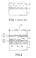
- FIG.1 shows a typical structure in which a thin buffer layer 2 of gallium arsenide is grown on a silicon wafer 1 and a gallium arsenide layer 3 serving as the substrate of semiconductor device.
- the buffer layer 2 is deposited on the silicon wafer 1 in the amorphous state for a thickness of about 100 - 200 ⁇ at a temperature of about 400 - 450°C and then the gallium arsenide layer 3 is grown for a thickness of about 3 - 5 ⁇ m.
- the gallium arsenide layer 3 is grown, the underlying gallium arsenide buffer layer 2 is crystallized into a single crystal phase and the gallium arsenide substrate layer 3 deposited thereon grows while maintaining epitaxial relation with the gallium arsenide buffer layer 2 underneath.
- the gallium arsenide layer 3 is grown successfully on the silicon wafer 1
- the dislocation density in the gallium arsenide layer grown on the substrate cannot be reduced below about 108/cm2.
- Such a dislocation occurs mainly at the interface between the silicon wafer 1 and the buffer layer 2 as illustrated in FIG.1 by a line 4, due to the lattice mismatch between silicon and GaAs.
- the buffer layer 2 is thus not effective in intercepting the propagation of the dislocations and the dislocations are extended into the gallium arsenide layer 3 on which the semiconductor devices are to be formed.
- dislocations are also created due to the surface defects or intrinsic defects involved in the wafer 1. The problem of the latter type of dislocations becomes conspicuous when a single crystal gallium arsenide wafer is used in place of the silicon wafer 1.
- the threshold voltage scatters unacceptably when the dislocation density exceeds about 106 cm ⁇ 2 and accordingly, the yield of the fabricated semiconductor device is inevitably decreased. Further, the existence of the dislocations causes a decrease of lifetime of the carrier or increase of the leak current across the p-n junction.
- the device is an optical semiconductor device such as laser diode, the optical output is also decreased.
- the dislocation density of a GaAs bulk crystal grown by Czochralski method can be reduced to about 100 cm ⁇ 2 by adding indium (In) with a concentration level of 2 X 1019 cm ⁇ 2 (Mil'vidsky, M.G., Osvensky, V.B. and Shifrin, S.S., J. Crystal. Growth, 52, p.396, 1981).
- the wafer sliced from such a bulk crystal has a composition of InGaAs and the utility of the wafer is limited.
- addition of In to the GaAs layer grown on another GaAs buffer layer as in the case of FIG.1 is generally unsuccessful as the addition of In with such an amount inevitably causes an unacceptable lattice mismatch.
- the growth of the GaAs layer containing In would create a significant amount of dislocations at the boundary to the underlying layer, with a worse result. Growth of another GaAs layer on the buffer layer thus added with In is not possible because of the same reason.
- Another object of the present invention is to provide a buffer structure interposed between an upper compound semiconductor layer and a lower material layer for intercepting propagation of dislocations from the underlying material layer to the overlying semiconductor layer.
- Another object of the present invention is to provide a buffer structure comprising a buffer layer interposed between an upper compound semiconductor layer and a lower material layer, wherein the buffer layer contains a group III element which is effective for intercepting dislocations, with a compositional profile which takes a maximum at a central part of the buffer structure and a minimum at top and bottom boundaries thereof respectively in contact to the upper compound semiconductor layer and the lower material layer.
- the buffer layer contains a group III element which is effective for intercepting dislocations, with a compositional profile which takes a maximum at a central part of the buffer structure and a minimum at top and bottom boundaries thereof respectively in contact to the upper compound semiconductor layer and the lower material layer.
- the lattice mismatch which would occur between the buffer layer and the compound semiconductor layer or between the buffer layer and the underlying material layer as a result of the admixing of the group III element is successfully avoided by providing the graded compositional profile to the buffer structure. Furthermore, creation of new dislocations at the boundary to the underlying layer or to the overlying layer is suppressed minimum because of the lattice matching thus achieved. As a result, a buffer structure which is effective for intercepting the propagation of the dislocations is obtained.
- the compositional profile of the buffer structure such that the content of the group III element changes stepwise, in other words, by constructing the buffer structure as a stacking of a number of thin layers each having its own content of the group III element, the dislocations are not only intercepted by the group III element but also trapped at the boundary between the layers and the efficiency of intercepting the dislocations is further improved.
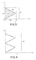
- FIG.2 showing a cross section of a compound semiconductor device 10 such as a field effect transistor (FET) constructed on the buffer structure of the present invention.
- FET field effect transistor
- the semiconductor device comprises a silicon substrate or wafer 11 on which a first buffer layer 12 of GaAs is grown for a thickness of 100 ⁇ , and on the first buffer layer 12, a first mixed crystal layer 13 of GaAs, a second buffer layer 14 of InGaAs constituting the essential part of the present invention and having a composition Ga 1-x In x As, and a second mixed crystal layer 15 of GaAs are grown successively with thickness of 1.5 ⁇ m, 0.2 ⁇ m, and 1.5 ⁇ m, respectively.
- the semiconductor device 10 is constructed on the second mixed crystal layer 15. In other words, it is desired to suppress the dislocation density in the layer 15 as low as possible.
- the first buffer layer 12 is in the amorphous phase when it is initially grown on the silicon wafer 11 but is later crystallized to a single crystal phase when the second buffer layer 13 is grown thereon.
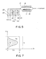
- FIG.3 shows a compositional profile of the second buffer layer 14.
- the axis y represents the thickness of the second buffer layer 14 measured perpendicularly to the substrate 11.
- the parameter x is increased stepwise by an amount of 0.1 in each 100 ⁇ thickness of the layer 14.
- the buffer layer 14 comprises a number of thin InGaAs layers 14a - 14t (FIG.2) each having its own In-content and a thickness of about 100 ⁇ .
- the distortion caused as a result of the lattice mismatch between Si and GaAs is absorbed by the first buffer layer 12 interposed between the silicon wafer 11 and the first mixed crystal layer 13.
- the first buffer layer 12 is grown in a form of the amorphous state and thus covers the surface of the silicon wafer 11 with reliability.
- the first mixed crystal layer 13 is grown thereon, the first buffer layer 12 is crystalized. Thereby, the dislocation density in the first mixed crystal layer 13 is reduced to about 108 cm ⁇ 2.
- This dislocation density is not acceptable for constructing semiconductor devices on the mixed crystal layer 13.
- Increase of the thickness of the first buffer layer 12 or the first mixed crystal layer 13 is not effective in reducing the dislocation density below the foregoing level, as the dislocations are propagated without substantial interception through these layers as shown in FIG.1.
- dislocations 41 (FIG.2) passed through the first buffer layer 12 and further through the first mixed crystal layer 13 are intercepted by In which is believed to induce a local strain in the host crystal structure, and the dislocations are trapped in such a strained region (Mil'vidsky et al. op.cit.).
- the In-content x is graded as shown in FIG.3 such that the parameter x is zero at the upper and lower boundary of the second buffer layer 14, the composition of the second buffer layer becomes identical to that of the underlying first mixed crystal layer 13 or the overlying second mixed crystal layer 15 and the problem of lattice mismatch at the upper and lower boundaries of the second buffer layer is eliminated.
- the stepwise increment of the In-content in the buffer structure of the present embodiment is particularly preferable from the view point of intercepting the dislocations effectively.
- measurement of the dislocation density of the mixed crystal layer 15 is undertaken by processing the structure of FIG.2 in a potassium hydrooxide (KOH) solution at 370°C for 10 minutes and counting the etch pits appearing on the surface of the layer 15, with a result that the dislocation density of 108 cm ⁇ 2 in the underlying GaAs layer 13 is reduced to 2 X 106 cm ⁇ 2 in the second mixed crystal layer 15. This level is acceptable for constructing a FET on the layer 15. In another measurement, it was observed that the dislocation density in the layer 15 is reduced to about 1 X 106 cm ⁇ 2.
- KOH potassium hydrooxide
- the dislocation density in the second mixed crystal layer 15 at the top of the structure is decreased further. From the foregoing observation, the dislocation density is decreased by a factor of 102 for each repetition of the compositional profile. Note that mere extension of the thickness of the second buffer layer 14, which causes formation of a region enriched in InAs at the central part of the layer 14, would be ineffective in intercepting the dislocations, as the interception of the dislocations is not caused by the In atom itself but the strain induced in the crystal structure of GaAs by the addition of In. In such an almost pure InAs structure, there would be no such strain in the structure.
- the element to be added to the buffer structure with the compositional profile of FIG.3 is not limited to In but other element different from Ga such as boron (B) or aluminium (Al) may also be used in the based buffer layer 14 as is supported by Mil'vidsky et al. (op. cit.).
- FIG.5 shows the general construction of a MOCVD apparatus used for growing the compound semiconductor layers in the structure of FIG.2.
- the silicon wafer 11 is placed on a susceptor 18 in a reaction chamber 17 and is heated together with the susceptor 18 by energization of a radio frequency coil 16.
- a suitable combination of arsine (AsH3), trimethyl gallium (TMG: (CH3)3Ga), and trimethyl indium (TMI: (CH3)3In) are introduced to the reaction chamber 17 together with a hydrogen (H2) carrier gas.
- AsH3 arsine
- TMG trimethyl gallium
- TMI trimethyl indium
- H2 hydrogen
- TMI and TMG are liquid in the normal state and are held in thermostatted containers 21 and 22 at a temperature of 15°C and 30°C, respectively.
- the gaseous molecules of TMG and TMI are supplied to the reaction chamber 17 through control valves 12 and 13. Further, arsine, held at a temperature of 0°C, is introduced to the reaction chamber 17 through a control valve 14.
- the silicon wafer 20 is held at 1000°C for about 10 minutes in the reaction chamber 17 and then the temperature of the wafer 11 is set to 450°C. Further, TMG and arsine are introduced to the reaction chamber 17. Thereby, the gaseous molecules thus introduced are reacted at the surface of the substrate 20 and the first buffer layer 22 is grown on the wafer 20 covering its surface in the amorphous state as shown in FIG.6(A).
- the temperature of the wafer 11 is raised to 700°C and TMG and arsine are introduced into the reaction chamber 17.
- the first mixed crystal layer 13 is grown on the first buffer layer 12 and a structure shown in FIG.6(B) is obtained.
- the previously grown amorphous buffer layer 22 is crystalized into a single crystal phase.
- the flow rate of arsine and TMG are set to 200 cc/min and 70 cc/min, respectively and a first layer 14a of the second buffer layer 14 which is free from In is grown on the first mixed crystal layer 13 for a thickness of about 100 ⁇ as shown in FIG.6(C).
- TMI is introduced further to TMG and arsine with a flow rate of 143 cc/min, and a structure shown in FIG.6(D) is obtained in which a second layer 14b having a composition Ga 0.9 In 0.1 As is grown on the first layer 14a.
- the flow rate of TMG and arsine are set similarly to the case of FIG.6(C).
- the flow rate of TMG and TMI stepwise a number of layers of InGaAs each having a thickness of about 100 ⁇ are grown one after another as shown in FIG.6(E) with a stepwise increment of the In-content.
- the In-content becomes maximum and the parameter x takes a value of 0.9.
- the composition of the InGaAs layer is represented as Ga 0.1 In 0.9 As.
- an eleventh layer 14k is grown on the tenth layer 14j with a composition identical to the layer 14j for a thickness of 100 ⁇ and further, other layers are grown thereon with a stepwise decrease of the In-content with a decrement of 0.1 in each layer by changing the ratio of TMG and TEI stepwise until a twentieth layer 14t is grown in which the In-content is zero as shown in FIG.6(F).
- the thickness of the layer is maintained at 100 ⁇ and thus, a symmetrical compositional profile having a maximum of the In-content at the center of the buffer layer 14 as shown in FIG.3 is obtained.
- the supply of TMI is stopped and the second mixed crystal layer 15 is grown while supplying arsine and TMG. As a result, the structure shown in FIG.2 is completed.
- the apparatus used for constructing the structures of FIGS. 6 (A) - (F) is of course not limited to the MOCVD apparatus of FIG.5 but a MBE apparatus may also be used.
- a stepwise compositional profile as shown in FIG.3 is easily obtained.
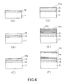
- a compositional profile shown in FIG.4 in which the In-content x is changed continuously instead of stepwise is also achieved.
- the dislocations are intercepted by the In atoms and at the same time, the lattice mismatch to the neighbouring layers 13 and 15 by incorporating In to the buffer layer 14 is avoided by providing the compositional gradation.
- the stepwise compositional increment is not limited to 0.1 as shown in FIG.3.
- the thickness of the layers 14a - 14t is not limited to 100 ⁇ either.
- a continuous compositional profile shown in FIG.7 is obtained as an extreme case in which the thickness of each layer is reduced to infinitesimal and the compositional increment of In is also reduced to infinitesimal. From the view point of trapping the dislocations at the boundary between the layers, however, it is preferred to form a distinct interface between the layers of the buffer layer 14 by providing the stepwise compositional profile.
- a stepwise increment of In-content of less than 0.1 and a layer thickness of more than 100 ⁇ are preferred, wherein the stepwise increment of 0.1 for the In-content and the layer thickness of 100 ⁇ as described are most preferred.
- the maximum of the In-content at the central part of the buffer layer 14 is not limited to 0.9 as described but may be smaller or larger and the central part of the buffer layer 14 may comprise pure InAs.
- the compositional profile of In is not necessarily be symmetrical about the central part of the buffer layer 14 but may be asymmetrical.
- the In-content at the top and bottom boundary of the buffer layer 14 is not necessarily be zero but may have a finite level unless unacceptable lattice mismatch is induced at the boundaries.
- the present invention includes also a case in which the first mixed crystal layer 13 and the second mixed crystal layer 15 have different compositions. In such a case, the compositional profile is asymmetric and the In-content may not be equal at the top boundary and at the bottom boundary of the buffer layer 14.
- the element incorporated to the GaAs buffer layer is not limited to In but other group III element such as B or Al may also be used.
- the present invention is effective also when the first buffer layer 12 comprises gallium phosphide (GaP) and the second buffer layer 14 comprises GaP added with In.
- the first and second mixed crystal layers 13 and 15 also comprises GaP and the second buffer layer 14 is provided with the compositional profile similar to FIG.3.
- the present invention is not limited to the buffer structure constructed on the silicon wafer but is applicable also to a case when growing a semiconductor layer free from dislocations or other defects on a semiconductor substrate or wafer of a same composition.
- the present invention is effective in growing a GaAs layer free from such defects on a GaAs wafer which usually contains a significant amount of detects.
- the GaAs wafer is used as the wafer 11 in the structure of FIG.2.
- the semiconductor material to be used as the wafer 11 and as the layers 13 and 15 in such a construction is not limited to GaAs but other materials such as germanium (Ge), gallium phosphide (GaP), gallium antimonide (GaSb), indium phosphide (InP), indium arsenide (InAs), indium antimonide (InSb), and the like may be used similarly.
- germanium Ga
- GaP gallium phosphide
- GaSb gallium antimonide
- InP indium phosphide
- InAs indium arsenide
- InSb indium antimonide
- the buffer layer 14 in the structure of FIG.2 comprises a compound semiconductor material containing Ga such as GaAs, GaP or GaSb
- elements such as In, B or Al are effective as the group III element for intercepting the dislocations
- the buffer layer 14 comprises a compound semiconductor material containing In such as InAs, InP or InSb
- elements such as Ga, B or Al are effective as the group III element in agreement with the report by Mil'vidsky et al. (op. cit.) for the case of bulk crystal.
- the content of the group III elements for intercepting the dislocations should be graded as shown in FIG.3, preferrably with stepwise profile.
Landscapes
- Recrystallisation Techniques (AREA)
- Junction Field-Effect Transistors (AREA)
- Semiconductor Lasers (AREA)
Applications Claiming Priority (2)
| Application Number | Priority Date | Filing Date | Title |
|---|---|---|---|
| JP325631/88 | 1988-12-22 | ||
| JP63325631A JPH02170413A (ja) | 1988-12-22 | 1988-12-22 | 化合物半導体装置 |
Publications (2)
| Publication Number | Publication Date |
|---|---|
| EP0375564A1 true EP0375564A1 (de) | 1990-06-27 |
| EP0375564B1 EP0375564B1 (de) | 1994-03-02 |
Family
ID=18179010
Family Applications (1)
| Application Number | Title | Priority Date | Filing Date |
|---|---|---|---|
| EP89403641A Expired - Lifetime EP0375564B1 (de) | 1988-12-22 | 1989-12-22 | Halbleiterbauelement mit einer Puffer-Struktur, um Defekte der darauf gewachsenen Halbleiterschicht aufzuheben |
Country Status (5)
| Country | Link |
|---|---|
| US (1) | US5134446A (de) |
| EP (1) | EP0375564B1 (de) |
| JP (1) | JPH02170413A (de) |
| KR (1) | KR930009805B1 (de) |
| DE (1) | DE68913479D1 (de) |
Cited By (5)
| Publication number | Priority date | Publication date | Assignee | Title |
|---|---|---|---|---|
| EP0425244A3 (en) * | 1989-10-23 | 1991-11-06 | Fujitsu Limited | Semiconductor device having a heteroepitaxial substrate |
| WO2002063665A3 (en) * | 2001-02-08 | 2003-01-23 | Amberwave Systems Corp | RELAXED InXGa1-xAs LAYERS INTEGRATED WITH Si |
| US6589335B2 (en) | 2001-02-08 | 2003-07-08 | Amberwave Systems Corporation | Relaxed InxGa1-xAs layers integrated with Si |
| US6594293B1 (en) | 2001-02-08 | 2003-07-15 | Amberwave Systems Corporation | Relaxed InxGa1-xAs layers integrated with Si |
| EP2732459A1 (de) * | 2011-07-12 | 2014-05-21 | NASP III/V GmbH | Monolithische integrierte halbleiterstruktur |
Families Citing this family (9)
| Publication number | Priority date | Publication date | Assignee | Title |
|---|---|---|---|---|
| CA2062134C (en) * | 1991-05-31 | 1997-03-25 | Ibm | Low Defect Densiry/Arbitrary Lattice Constant Heteroepitaxial Layers |
| JP3116731B2 (ja) * | 1994-07-25 | 2000-12-11 | 株式会社日立製作所 | 格子不整合系積層結晶構造およびそれを用いた半導体装置 |
| US6423990B1 (en) * | 1997-09-29 | 2002-07-23 | National Scientific Corporation | Vertical heterojunction bipolar transistor |
| US5912481A (en) | 1997-09-29 | 1999-06-15 | National Scientific Corp. | Heterojunction bipolar transistor having wide bandgap, low interdiffusion base-emitter junction |
| US6087683A (en) * | 1998-07-31 | 2000-07-11 | Lucent Technologies | Silicon germanium heterostructure bipolar transistor with indium doped base |
| KR100355636B1 (ko) * | 2000-03-10 | 2002-10-11 | 광주과학기술원 | 인듐갈륨알소나이드 콜렉터 에이치비티의 에피택시얼구조 |
| US7227174B2 (en) * | 2003-06-26 | 2007-06-05 | Rj Mears, Llc | Semiconductor device including a superlattice and adjacent semiconductor layer with doped regions defining a semiconductor junction |
| JP4333426B2 (ja) * | 2004-03-19 | 2009-09-16 | ソニー株式会社 | 化合物半導体の製造方法、及び半導体装置の製造方法 |
| CN119050812B (zh) * | 2024-08-23 | 2025-08-26 | 中国科学院西安光学精密机械研究所 | 一种o波段硅基三五族量子点窄线宽激光器及其制备方法 |
Citations (1)
| Publication number | Priority date | Publication date | Assignee | Title |
|---|---|---|---|---|
| US3821033A (en) * | 1972-08-03 | 1974-06-28 | Ibm | Method for producing flat composite semiconductor substrates |
Family Cites Families (6)
| Publication number | Priority date | Publication date | Assignee | Title |
|---|---|---|---|---|
| US4568958A (en) * | 1984-01-03 | 1986-02-04 | General Electric Company | Inversion-mode insulated-gate gallium arsenide field-effect transistors |
| JPH0650723B2 (ja) * | 1984-10-17 | 1994-06-29 | 日本電気株式会社 | エピタキシヤル成長方法 |
| US4768074A (en) * | 1984-11-20 | 1988-08-30 | Kabushiki Kaisha Toshiba | Heterojunction bipolar transistor having an emitter region with a band gap greater than that of a base region |
| US4872046A (en) * | 1986-01-24 | 1989-10-03 | University Of Illinois | Heterojunction semiconductor device with <001> tilt |
| US4806996A (en) * | 1986-04-10 | 1989-02-21 | American Telephone And Telegraph Company, At&T Bell Laboratories | Dislocation-free epitaxial layer on a lattice-mismatched porous or otherwise submicron patterned single crystal substrate |
| US4769341A (en) * | 1986-12-29 | 1988-09-06 | American Telephone And Telegraph Company, At&T Bell Laboratories | Method of fabricating non-silicon materials on silicon substrate using an alloy of Sb and Group IV semiconductors |
-
1988
- 1988-12-22 JP JP63325631A patent/JPH02170413A/ja active Pending
-
1989
- 1989-12-22 KR KR1019890019297A patent/KR930009805B1/ko not_active Expired - Fee Related
- 1989-12-22 DE DE89403641T patent/DE68913479D1/de not_active Expired - Lifetime
- 1989-12-22 EP EP89403641A patent/EP0375564B1/de not_active Expired - Lifetime
-
1991
- 1991-07-01 US US07/725,889 patent/US5134446A/en not_active Expired - Fee Related
Patent Citations (1)
| Publication number | Priority date | Publication date | Assignee | Title |
|---|---|---|---|---|
| US3821033A (en) * | 1972-08-03 | 1974-06-28 | Ibm | Method for producing flat composite semiconductor substrates |
Non-Patent Citations (4)
| Title |
|---|
| APPLIED PHYSICS LETTERS * |
| JOURNAL OF VACUUM SCIENCE & TECHNOLOGY/SECTION B * |
| PATENT ABSTRACTS OF JAPAN * |
| RESEARCH DISCLOSURE * |
Cited By (5)
| Publication number | Priority date | Publication date | Assignee | Title |
|---|---|---|---|---|
| EP0425244A3 (en) * | 1989-10-23 | 1991-11-06 | Fujitsu Limited | Semiconductor device having a heteroepitaxial substrate |
| WO2002063665A3 (en) * | 2001-02-08 | 2003-01-23 | Amberwave Systems Corp | RELAXED InXGa1-xAs LAYERS INTEGRATED WITH Si |
| US6589335B2 (en) | 2001-02-08 | 2003-07-08 | Amberwave Systems Corporation | Relaxed InxGa1-xAs layers integrated with Si |
| US6594293B1 (en) | 2001-02-08 | 2003-07-15 | Amberwave Systems Corporation | Relaxed InxGa1-xAs layers integrated with Si |
| EP2732459A1 (de) * | 2011-07-12 | 2014-05-21 | NASP III/V GmbH | Monolithische integrierte halbleiterstruktur |
Also Published As
| Publication number | Publication date |
|---|---|
| US5134446A (en) | 1992-07-28 |
| KR930009805B1 (ko) | 1993-10-11 |
| DE68913479D1 (de) | 1994-04-07 |
| JPH02170413A (ja) | 1990-07-02 |
| KR900010924A (ko) | 1990-07-11 |
| EP0375564B1 (de) | 1994-03-02 |
Similar Documents
| Publication | Publication Date | Title |
|---|---|---|
| EP0375564B1 (de) | Halbleiterbauelement mit einer Puffer-Struktur, um Defekte der darauf gewachsenen Halbleiterschicht aufzuheben | |
| US5144379A (en) | Semiconductor device having a group iii-v epitaxial semiconductor layer on a substrate | |
| US7115896B2 (en) | Semiconductor structures for gallium nitride-based devices | |
| US4963949A (en) | Substrate structures for InP-based devices | |
| EP0097772B1 (de) | Struktur mit monokristallinem Substrat als Träger für eine Halbleiterschicht für eine Anordnung | |
| EP0331467B1 (de) | Methode zur Erzeugung einer halbleitenden Dünnschicht | |
| JP3093904B2 (ja) | 化合物半導体結晶の成長方法 | |
| EP0279989B1 (de) | Halbleiter-Heterostruktur mit einem Bereich mit veränderlicher SnSi Verbindung | |
| KR100319300B1 (ko) | 이종접합구조의 양자점 버퍼층을 가지는 반도체 소자 | |
| US5402748A (en) | Method of growing a compound semiconductor film | |
| KR101151933B1 (ko) | 화합물 반도체 에피택셜 기판 및 그 제조 방법 | |
| US5599389A (en) | Compound semiconductor and method of manufacturing the same | |
| EP0291346A2 (de) | Mehrschichtige Struktur aus halbleitenden Verbindungen | |
| EP0402209A1 (de) | Halbleiterbauelement mit einer auf einem Substrat aufgewachsenen epitaxialen Schicht | |
| EP0430562B1 (de) | Halbleiterheterostruktur und Verfahren zu ihrer Herstellung | |
| US7588954B2 (en) | InGaAs/GaAs lasers on silicon produced by LEPECVD and MOCVD | |
| US5456206A (en) | Method for two-dimensional epitaxial growth of III-V compound semiconductors | |
| US20090045437A1 (en) | Method and apparatus for forming a semi-insulating transition interface | |
| US5183776A (en) | Heteroepitaxy by growth of thermally strained homojunction superlattice buffer layers | |
| Fan | Thin films of III-V compounds and their applications | |
| EP0416128B1 (de) | Plättchen aus halbleiterkomposit | |
| JP2980630B2 (ja) | 化合物半導体装置 | |
| US8906158B2 (en) | Method for producing compound semiconductor epitaxial substrate having PN junction | |
| JPH01211912A (ja) | 半導体基板 | |
| JPH04199507A (ja) | 3―V族化合物半導体へのn型不純物固相拡散方法 |
Legal Events
| Date | Code | Title | Description |
|---|---|---|---|
| PUAI | Public reference made under article 153(3) epc to a published international application that has entered the european phase |
Free format text: ORIGINAL CODE: 0009012 |
|
| AK | Designated contracting states |
Kind code of ref document: A1 Designated state(s): DE FR GB |
|
| 17P | Request for examination filed |
Effective date: 19901221 |
|
| 17Q | First examination report despatched |
Effective date: 19920603 |
|
| GRAA | (expected) grant |
Free format text: ORIGINAL CODE: 0009210 |
|
| AK | Designated contracting states |
Kind code of ref document: B1 Designated state(s): DE FR GB |
|
| PG25 | Lapsed in a contracting state [announced via postgrant information from national office to epo] |
Ref country code: DE Effective date: 19940302 |
|
| REF | Corresponds to: |
Ref document number: 68913479 Country of ref document: DE Date of ref document: 19940407 |
|
| ET | Fr: translation filed | ||
| PG25 | Lapsed in a contracting state [announced via postgrant information from national office to epo] |
Ref country code: GB Effective date: 19941222 |
|
| PLBE | No opposition filed within time limit |
Free format text: ORIGINAL CODE: 0009261 |
|
| STAA | Information on the status of an ep patent application or granted ep patent |
Free format text: STATUS: NO OPPOSITION FILED WITHIN TIME LIMIT |
|
| 26N | No opposition filed | ||
| GBPC | Gb: european patent ceased through non-payment of renewal fee |
Effective date: 19941222 |
|
| PGFP | Annual fee paid to national office [announced via postgrant information from national office to epo] |
Ref country code: FR Payment date: 19981209 Year of fee payment: 10 |
|
| PG25 | Lapsed in a contracting state [announced via postgrant information from national office to epo] |
Ref country code: FR Free format text: LAPSE BECAUSE OF NON-PAYMENT OF DUE FEES Effective date: 20000831 |
|
| REG | Reference to a national code |
Ref country code: FR Ref legal event code: ST |