EP0376709A2 - Procédé de fabrication d'un dispositif semi-conducteur par pulvérisation du métal - Google Patents
Procédé de fabrication d'un dispositif semi-conducteur par pulvérisation du métal Download PDFInfo
- Publication number
- EP0376709A2 EP0376709A2 EP89313630A EP89313630A EP0376709A2 EP 0376709 A2 EP0376709 A2 EP 0376709A2 EP 89313630 A EP89313630 A EP 89313630A EP 89313630 A EP89313630 A EP 89313630A EP 0376709 A2 EP0376709 A2 EP 0376709A2
- Authority
- EP
- European Patent Office
- Prior art keywords
- substrate
- temperature
- sputtering
- material layer
- voltage
- Prior art date
- Legal status (The legal status is an assumption and is not a legal conclusion. Google has not performed a legal analysis and makes no representation as to the accuracy of the status listed.)
- Withdrawn
Links
Images



Classifications
-
- C—CHEMISTRY; METALLURGY
- C23—COATING METALLIC MATERIAL; COATING MATERIAL WITH METALLIC MATERIAL; CHEMICAL SURFACE TREATMENT; DIFFUSION TREATMENT OF METALLIC MATERIAL; COATING BY VACUUM EVAPORATION, BY SPUTTERING, BY ION IMPLANTATION OR BY CHEMICAL VAPOUR DEPOSITION, IN GENERAL; INHIBITING CORROSION OF METALLIC MATERIAL OR INCRUSTATION IN GENERAL
- C23C—COATING METALLIC MATERIAL; COATING MATERIAL WITH METALLIC MATERIAL; SURFACE TREATMENT OF METALLIC MATERIAL BY DIFFUSION INTO THE SURFACE, BY CHEMICAL CONVERSION OR SUBSTITUTION; COATING BY VACUUM EVAPORATION, BY SPUTTERING, BY ION IMPLANTATION OR BY CHEMICAL VAPOUR DEPOSITION, IN GENERAL
- C23C14/00—Coating by vacuum evaporation, by sputtering or by ion implantation of the coating forming material
- C23C14/22—Coating by vacuum evaporation, by sputtering or by ion implantation of the coating forming material characterised by the process of coating
- C23C14/34—Sputtering
-
- H—ELECTRICITY
- H10—SEMICONDUCTOR DEVICES; ELECTRIC SOLID-STATE DEVICES NOT OTHERWISE PROVIDED FOR
- H10W—GENERIC PACKAGES, INTERCONNECTIONS, CONNECTORS OR OTHER CONSTRUCTIONAL DETAILS OF DEVICES COVERED BY CLASS H10
- H10W20/00—Interconnections in chips, wafers or substrates
- H10W20/01—Manufacture or treatment
- H10W20/031—Manufacture or treatment of conductive parts of the interconnections
- H10W20/056—Manufacture or treatment of conductive parts of the interconnections by filling conductive material into holes, grooves or trenches
- H10W20/059—Manufacture or treatment of conductive parts of the interconnections by filling conductive material into holes, grooves or trenches by reflowing or applying pressure
-
- C—CHEMISTRY; METALLURGY
- C23—COATING METALLIC MATERIAL; COATING MATERIAL WITH METALLIC MATERIAL; CHEMICAL SURFACE TREATMENT; DIFFUSION TREATMENT OF METALLIC MATERIAL; COATING BY VACUUM EVAPORATION, BY SPUTTERING, BY ION IMPLANTATION OR BY CHEMICAL VAPOUR DEPOSITION, IN GENERAL; INHIBITING CORROSION OF METALLIC MATERIAL OR INCRUSTATION IN GENERAL
- C23C—COATING METALLIC MATERIAL; COATING MATERIAL WITH METALLIC MATERIAL; SURFACE TREATMENT OF METALLIC MATERIAL BY DIFFUSION INTO THE SURFACE, BY CHEMICAL CONVERSION OR SUBSTITUTION; COATING BY VACUUM EVAPORATION, BY SPUTTERING, BY ION IMPLANTATION OR BY CHEMICAL VAPOUR DEPOSITION, IN GENERAL
- C23C14/00—Coating by vacuum evaporation, by sputtering or by ion implantation of the coating forming material
- C23C14/06—Coating by vacuum evaporation, by sputtering or by ion implantation of the coating forming material characterised by the coating material
- C23C14/14—Metallic material, boron or silicon
- C23C14/18—Metallic material, boron or silicon on other inorganic substrates
-
- C—CHEMISTRY; METALLURGY
- C23—COATING METALLIC MATERIAL; COATING MATERIAL WITH METALLIC MATERIAL; CHEMICAL SURFACE TREATMENT; DIFFUSION TREATMENT OF METALLIC MATERIAL; COATING BY VACUUM EVAPORATION, BY SPUTTERING, BY ION IMPLANTATION OR BY CHEMICAL VAPOUR DEPOSITION, IN GENERAL; INHIBITING CORROSION OF METALLIC MATERIAL OR INCRUSTATION IN GENERAL
- C23C—COATING METALLIC MATERIAL; COATING MATERIAL WITH METALLIC MATERIAL; SURFACE TREATMENT OF METALLIC MATERIAL BY DIFFUSION INTO THE SURFACE, BY CHEMICAL CONVERSION OR SUBSTITUTION; COATING BY VACUUM EVAPORATION, BY SPUTTERING, BY ION IMPLANTATION OR BY CHEMICAL VAPOUR DEPOSITION, IN GENERAL
- C23C14/00—Coating by vacuum evaporation, by sputtering or by ion implantation of the coating forming material
- C23C14/22—Coating by vacuum evaporation, by sputtering or by ion implantation of the coating forming material characterised by the process of coating
- C23C14/54—Controlling or regulating the coating process
- C23C14/541—Heating or cooling of the substrates
-
- H—ELECTRICITY
- H10—SEMICONDUCTOR DEVICES; ELECTRIC SOLID-STATE DEVICES NOT OTHERWISE PROVIDED FOR
- H10W—GENERIC PACKAGES, INTERCONNECTIONS, CONNECTORS OR OTHER CONSTRUCTIONAL DETAILS OF DEVICES COVERED BY CLASS H10
- H10W20/00—Interconnections in chips, wafers or substrates
- H10W20/01—Manufacture or treatment
- H10W20/031—Manufacture or treatment of conductive parts of the interconnections
- H10W20/062—Manufacture or treatment of conductive parts of the interconnections by smoothing of conductive parts, e.g. by planarisation
Definitions
- the present invention generally relates to fabrication of semiconductor devices and more particularly to a method of providing a planarized, long-lifetime metallizations and interconnections on a stepped surface of a material layer constituting a semiconductor device.
- various materials are used for interconnecting and metallizing devices in semiconductor integrated circuits. These materials include pure aluminium, aluminium alloy of various compositions, refractory metals such as titanium (Ti), tungsten (W), molybdenum (Mo), copper (Cu) and the like, alloy or mixture of these refractory metals, compounds of refractory metals combined with other elements such as silicides of Mo or W, and the like. These materials are usually deposited on a material layer or a substrate constituting the semiconductor device by sputtering.
- the substrate or material layer on which a conductor layer of the foregoing materials is to be provided for interconnection or metallization tends to have a surface defined with minute steps.
- the aspect ratio of a through hole provided for interconnection between a conductor layer on a top side of the substrate and another conductor layer below the substrate is increased with decreasing hole dimension.
- the aspect ratio is defined as a step height of the hole divided by the hole diameter.
- Responsive thereto there is a difficulty in forming the conductor layer by sputtering such that the conductor layer fills the through hole or covers the steps with excellent step coverage.
- the poor step coverage becomes an acute problem when a multi-level interconnection or metallization structure is to be constructed.
- the conductor layer has a planarized top surface irrespective of whether the conductor layer covers a flat part or stepped part of the substrate such as the through hole.
- a so-called bias sputtering technique is proposed recently in which deposition of the conductor layer is made while applying a negative bias voltage to the substrate.
- atoms of sputtered conductor material maintain a sufficient thermal and kinetic energy even after arrival at the surface and move along the surface of the substrate relatively freely.
- a sputter-etching of the conductor layer is performed simultaneously to the deposition.
- any depression in the sputtered conductor layer is filled by the atoms of the conductor material moving laterally along its surface and any sharp projections on the surface which may become a nuclei of rough surface is constantly flattened as a result of the sputter-etching.
- the conductor layer is deposited on the stepped part of the substrate with an improved step coverage.
- Al or Al alloy such as Al-1%Si, Al-1%Si-O.5%Cu, Al-2.0%Cu, and the like
- the negative bias voltage applied to the substrate is in the order of -400 - -600 volts.
- a further improved step coverage is obtained by maintaining the substrate at a temperature of 200 - 300°C.
- the applicants made experiments of bias sputtering under various conditions including the foregoing region and made a discovery that the Ar-content in the deposited conductor layer decreases significantly and suddenly, contrary to the prediction, when the condition of sputtering has entered into the foregoing region where the substrate temperature exceeds about 400°C and the negative bias voltage exceeds about -400 volts in the negative direction (Hariu, T., Watanabe, K., Inoue, M., Takada, T., Tsuchikawa, H., IEEE/IRPS, April 1989, published later than the priority date claimed in the present application), which discovery constitutes the basis of the present invention.
- Another and more specific object of the present invention is to provide a method of depositing a conductor layer on a stepped surface by a bias-sputtering technique with an excellent step coverage.
- Another object of the present invention is to provide a method of depositing a conductor layer on a stepped surface of a substrate by a bias-sputtering technique for interconnecting or metallizing semiconductor devices, wherein the reliability of interconnection and metallization is improved.
- Another object of the present invention is to provide a method of depositing a conductor layer on a stepped surface by a bias-sputtering technique with an excellent planarization of a top surface of the deposited conductor layer.
- Another object of the present invention is to provide a method of depositing a conductor layer on a stepped surface of a substrate by sputtering undertaken in an inert atmosphere with a negative bias voltage applied to the substrate, wherein the substrate is held at a temperature higher than a critical temperature above which the content of Ar is reduced substantially below about 1 atomic percent (atm%), or above which a ratio of step coverage, defined as a minimum thickness of the conductor layer divided by a layer thickness of the conductor layer on a flat part of the substrate, is increased stepwise, and the sputtering is performed under a negative bias voltage with a magnitude set larger than that of a critical bias voltage above which the ratio of step coverage increases stepwise.
- the step coverage is improved significantly to a near-ideal extent. Further, the defects in the conductor layer caused by the impinged Ar is reduced significantly. Associated therewith, the reliability of interconnection or metallization structure is improved and the planarization of the structure is achieved simultaneously.
- FIG.1 shows the apparatus used for the bias sputtering experiment.
- the apparatus comprises a sputtering chamber 10 having an inlet 11 for introducing Ar gas and an outlet for evacuating the sputtering chamber 10.
- a sputtering chamber 10 having an inlet 11 for introducing Ar gas and an outlet for evacuating the sputtering chamber 10.
- an 8-inch diameter target 13 of Al or other material to be sputtered and the target 13 is applied with a d.c. bias voltage by a DC power source 14.
- a substrate 16 Facing the target 13, a substrate 16 is held on a substrate holder 17 which in turn is provided on a side of the chamber 10 opposing the side on which the target 13 is provided, and the substrate 16 is applied with a radio frequency (r.f.) energization from an RF power source 18 via an impedance matching circuit 19 as well as via the substrate holder 17.
- the radio frequency energization generated by the RF source 18 has a frequency of statutory prescribed 13.56 MHz and induces a selective accumulation of electrons in the substrate 16, thereby applying a negative d.c. bias voltage to the substrate 16.
- the negative d.c. bias voltage is controlled by changing the power of the r.f. energization while measuring the bias voltage directly by a voltage meter 20.
- the construction of the substrate 16 is identical to that of the target of a typical r.f. sputtering apparatus.
- collision of the positively charged Ar ions to the substrate 16 causes a sputtering evaporation or sputter-etching of the substrate, and the deposition of the material on the substrate 16 from the target 16 proceeds simultaneously to the etching of the substrate 16.
- sharp projections on the material layer deposited on the surface of the substrate 16 is selectively etched and a flat, smooth surface is obtained.
- the holder 17 is provided with a heater 21 for controlling the temperature of the substrate 16.
- the holder 17 is constructed to have a hollow structure, and the heater 21 is used to heat the argon gas in the hollow structure which transports the heat to the substrate efficiently.
- the Ar gas is used in this case as a heating medium. Further, it may be possible to heat the substrate 16 by directly flowing the current to the holder 17.
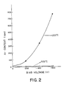
- FIG.2 shows a result of experiments conducted for an Al alloy having a composition of Al-2.0%Cu while changing the negative bias voltage from -200 volts to -600 volts.
- the bias voltage is controlled by changing the output r.f. power of the RF source 18 while monitoring the voltage meter 20.
- the substrate 16 used for the experiment was an (100) oriented silicon wafer with a phosphosilicate glass (PSG) layer having a thickness of 1.0 ⁇ m which in turn is covered by a titanium (Ti) layer with a thickness of 200 ⁇ .
- PSG phosphosilicate glass
- Ti titanium
- Such a droplet is formed as a result of the surface tension of the Al alloy or other metals provided on the surface of the PSG layer.
- These sputtered metals have an increased fluidity when the temperature of sputtering is high and close to the melting point of the sputtered material.
- a refractory metal layer such as the Ti layer having the high melting point on the PSG layer
- the wettability of the sputtered metal layer is improved.
- Another reason of providing the Ti layer is to reduce the thermal radiation from the deposited layer and to obtain a higher surface temperature of the substrate. As a result, the particles arrived at the surface of the substrate retain a sufficient energy and move freely.
- the material for covering the PSG layer is not limited to Ti but other refractory materials such as W, titanium tungstenide (TiW), Mo, tantalum (Ta), niobium (Nb), and the like may be used provided that the refractory material has a melting point higher than that of the material to be deposited thereon.
- the thickness of the foregoing refractory materials is not limited to 200 ⁇ but may be several hundred angstroms.
- the substrate 16 was held at a temperature of 200°C and the sputtering was performed for 35 seconds with a d.c. sputtering power of 13 kW under a flow rate of Ar set at 80 sccm while increasing the bias voltage from zero volt in the negative direction.
- the temperature of the substrate 16 was set at 500°C and the sputtering was repeated under a same condition except for the temperature.
- the content of Ar in the sputter deposited Al alloy layer is increased in the first series experiments at 200°C with the increasing bias voltage.
- the content of Ar in FIG.2 is represented as the number of counts (c.p.s.) of the K ⁇ radiation emitted by the Ar atoms in the alloy layer in a unit time upon excitation by a characteristic X-ray radiation from a chromium (Cr) target.
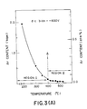
- FIG.3(A) shows the result of this research.
- the content of Ar is represented by the number of counts of the fluorescent K ⁇ X-ray radiation emitted from Ar. Note that the absolute scale for the count does not coincide each other in FIG.2 and in FIG.3(A) because of the difference in the condition at the time of measurement. For the data point corresponding to the substrate temperature of 200°C and the d.c.
- the temperature region in FIG.3(A) is divided by the critical temperature A into a first region I where the gradient is steep and a second region II where the gradient is gentle.
- the region II is not only characterized by the gentle slope of the curve but also by the Ar-content which is substantially smaller than 1 atm%, probably less than 0.5 atm%.
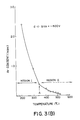
- FIG.3(B) shows a graph similar to FIG.3(A) for another series of experiments undertaken at the bias voltage set at -600 volts.
- the temperature region is divided into the region I and the region II, though the critical temperature separating the region II from the region I is shifted slightly lower to a temperature of about 350°C.
- the foregoing values of the critical temperature itself may not be the absolute measure of the division of the region I and the region II as such a value may be changed depending on the sputtering condition.
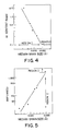
- FIG.4 shows a relation between the Ar content represented by the number of counts of XRF radiation and a median grain size. Note that the grain size measurement was performed by the TEM observation of the grains in the sputtered layer and each dot in FIG.4 corresponds to the experimental point in FIG.3(A), though not all of the experimental points are represented in FIG.4 because of the clarity of the drawing. From FIG.4, it is clear that there is a distinct correlation between the Ar content and the median grain size. In the region II where the Ar-content measured by the number of counts of the XRF radiation is characteristically smaller than about 0.1 kcps, the mean grain size becomes equal to or larger than about 10,000 ⁇ while in the region I, the median grain size becomes substantially smaller than 10,000 ⁇ .
- FIG.5 shows a relation observed between the median grain size and the MTF.
- the samples used for this experiment had a width of 2.0 ⁇ m, a length of 800 ⁇ m, and a thickness of 1 ⁇ m.
- the MTF was measured by flowing a d.c. current with a current density of 2.0 X 10⁶ A/cm2 at a temperature of 200°C.
- the time-to-failure herein is defined as a time at which the resistivity of the sputtered conductor layer is doubled with respect to the initial resistivity value, and the MTF value was determined by applying the Weibull distribution to the obtained time-to-failure data.
- TABLE I rearranges the data of MTF in FIG.5 into a combination of the bias voltage and the substrate temperature at the time of sputtering.
- the MTF decreases significantly with the bias voltage when the temperature of the substrate is held at 200°C while it does not change significantly with the bias voltage when the temperature is held at 500°C, in agreement with the relation shown in FIG.2.
- MTF is correlated to the Ar-content as already described.
- the parameter R in FIG.6 is much larger than the parameter R in FIG.7.
- FIGS.8(A) and (B) show the result of measurement for the parameter R in the sputtered alloy layer of Al-2.0%Cu covering the foregoing through hole 33 while changing the condition of sputtering similarly to the foregoing cases shown in FIGS.2 and 3(A).
- the temperature of the substrate 31 was changed from room temperature to 600°C while maintaining the bias voltage at -600 volts as shown in FIG.8(A), and the bias voltage was changed from zero volt to -600 volts while maintaining the temperature of the substrate 31 at 500°C as shown in FIG.8(B).
- the stepwise increase of the step coverage at the critical temperature B in FIG.8(A) is related to the change of the rate of decrease of the Ar-content at the critical temperature A in FIG.3(A) and that the critical temperature A and the critical temperature B represent a same boundary.
- the rate of step coverage R is below about 30 % while in the region II′, the parameter R is above 90 %.
- the parameter R jumps about three times across the critical temperature B.
- the rate of change of the parameter R in a 100°C temperature interval or the slope of the curve of FIG.8(A) increases from about 10%/100°C to about 70%/100°C at the temperature B. This increase of the slope is about seven times.
- FIG.8(B) shows that there is also a stepwise increase in the rate of step coverage R with the bias voltage across a critical voltage indicated by an arrow °C.
- This voltage C is located somewhere between -300 - -400 volts, probably close to -300 volts and the parameter R jumps from a first value of about 25 % in a region A below the voltage C to a second value of about 60 % or more in a region B above the voltage C with a factor of more than 2.
- the bias voltage is increased to about -500 - -600 volts, the parameter R reaches a level of 90 % or more.
- a reliable, low Ar-content, near-ideally planarized interconnection or metallization layer shown in FIG.6 or FIG.8(B), which constitutes the first embodiment of the present invention is obtained by sputtering the conductor material under a negative bias voltage and a substrate temperature set so as to fall in the region II for the temperature and in the region B for the bias voltage.
- the region II is characterized by the Ar-content substantially lower than about 1%, the median grain size of larger than about 10,000 ⁇ , and the rate of step coverage R of at least larger than 50 %, while the region B is characterized by the rate of step coverage R larger than 50 %.
- FIG.9 summarizes graphically the relation described heretofore.
- the boundary 101 is by no means an arbitrarily drawn hypothetical boundary across which the property changes without remarkable event but does reflect a qualitative and quantitative change of the phenomenon taking place during the sputtering.
- FIGS.10 and 11 a second embodiment of the present invention will be described with reference to FIGS.10 and 11.
- these parts already described with reference to the preceding drawings are given identical reference numerals and the description thereof will be omitted.
- W is used as the target 13 in the apparatus of FIG.1 and a layer of W is deposited for a thickness of about 0.5 ⁇ m, for example, on a PSG layer 32 including a through hole 33, which now has a diameter of 1.6 ⁇ m.
- the temperature of the substrate 31 is held at 450°C and a negative bias voltage of -1000 volts is applied to the substrate 31 during the sputtering.
- the r.f. power generated by the RF source 18 in correspondence to this voltage may be set to 200 W.
- the DC source 14 for establishing the plasma is driven with a power of 7 kW and the Ar gas is supplied to the chamber 10 with a flow rate of 40 sccm. Under this condition, the conductor layer 36 shown in FIG.11 having an excellent step coverage is obtained.
- the magnitude of the negative bias voltage applied to the substrate is preferrably larger than about 1000 volts in correspondence to the large energy needed for moving the atoms as compared to the case of Al or Al alloys.
- the magnitude is preferable to be smaller than about 2000 volts in order to avoid excessive etching effect which reduces the growth rate of the deposited film.
- the thickness or number of layers deposited by the present invention is of course not limited to those described heretofore.
- the present invention is useful in multi-layered interconnection and metallization structure.
- the inert gas used in the sputtering is not limited to Ar but other inert gases such as neon may also be used.
- the method of the present invention is not only useful in the interconnection and metallization structures but may also be used for providing gate electrode or buried electrode in the three-dimensional devices.
Landscapes
- Chemical & Material Sciences (AREA)
- Chemical Kinetics & Catalysis (AREA)
- Engineering & Computer Science (AREA)
- Materials Engineering (AREA)
- Mechanical Engineering (AREA)
- Metallurgy (AREA)
- Organic Chemistry (AREA)
- Inorganic Chemistry (AREA)
- Electrodes Of Semiconductors (AREA)
- Internal Circuitry In Semiconductor Integrated Circuit Devices (AREA)
- Physical Vapour Deposition (AREA)
Applications Claiming Priority (2)
| Application Number | Priority Date | Filing Date | Title |
|---|---|---|---|
| JP63331157A JPH02178923A (ja) | 1988-12-29 | 1988-12-29 | 半導体装置の製造方法 |
| JP331157/88 | 1988-12-29 |
Publications (2)
| Publication Number | Publication Date |
|---|---|
| EP0376709A2 true EP0376709A2 (fr) | 1990-07-04 |
| EP0376709A3 EP0376709A3 (fr) | 1990-10-10 |
Family
ID=18240511
Family Applications (1)
| Application Number | Title | Priority Date | Filing Date |
|---|---|---|---|
| EP19890313630 Withdrawn EP0376709A3 (fr) | 1988-12-29 | 1989-12-28 | Procédé de fabrication d'un dispositif semi-conducteur par pulvérisation du métal |
Country Status (3)
| Country | Link |
|---|---|
| EP (1) | EP0376709A3 (fr) |
| JP (1) | JPH02178923A (fr) |
| KR (1) | KR930010969B1 (fr) |
Cited By (5)
| Publication number | Priority date | Publication date | Assignee | Title |
|---|---|---|---|---|
| EP0543254A3 (en) * | 1991-11-22 | 1993-12-08 | St Microelectronics Srl | A method of forming high-stability metallic contacts in an integrated circuit with one or more metallized layers |
| EP0595624A1 (fr) * | 1992-10-28 | 1994-05-04 | Nihon Shinku Gijutsu Kabushiki Kaisha | Appareil à former des films, pour obturer les pores fins d'un substrat |
| EP0574687A3 (en) * | 1992-05-20 | 1994-05-18 | Siemens Ag | Method of depositing a planar layer containing aluminium on a substrate with a hole structure in its surface |
| US6155198A (en) * | 1994-11-14 | 2000-12-05 | Applied Materials, Inc. | Apparatus for constructing an oxidized film on a semiconductor wafer |
| CN119403138A (zh) * | 2024-12-31 | 2025-02-07 | 甬江实验室 | 半导体结构及其制备方法、芯片 |
Families Citing this family (2)
| Publication number | Priority date | Publication date | Assignee | Title |
|---|---|---|---|---|
| JPH04363024A (ja) * | 1990-11-30 | 1992-12-15 | Toshiba Corp | 半導体装置の製造方法 |
| JP2725944B2 (ja) * | 1991-04-19 | 1998-03-11 | インターナショナル・ビジネス・マシーンズ・コーポレイション | 金属層堆積方法 |
Family Cites Families (1)
| Publication number | Priority date | Publication date | Assignee | Title |
|---|---|---|---|---|
| JPH069199B2 (ja) * | 1984-07-18 | 1994-02-02 | 株式会社日立製作所 | 配線構造体およびその製造方法 |
-
1988
- 1988-12-29 JP JP63331157A patent/JPH02178923A/ja active Pending
-
1989
- 1989-12-28 EP EP19890313630 patent/EP0376709A3/fr not_active Withdrawn
- 1989-12-29 KR KR1019890020121A patent/KR930010969B1/ko not_active Expired - Fee Related
Cited By (7)
| Publication number | Priority date | Publication date | Assignee | Title |
|---|---|---|---|---|
| EP0543254A3 (en) * | 1991-11-22 | 1993-12-08 | St Microelectronics Srl | A method of forming high-stability metallic contacts in an integrated circuit with one or more metallized layers |
| US6350676B1 (en) | 1991-11-22 | 2002-02-26 | Sgs-Thomson Microelectronics, S.R.L. | Method of forming high-stability metallic contacts in an integrated circuit with one or more metallized layers |
| EP0574687A3 (en) * | 1992-05-20 | 1994-05-18 | Siemens Ag | Method of depositing a planar layer containing aluminium on a substrate with a hole structure in its surface |
| US6033534A (en) * | 1992-05-20 | 2000-03-07 | Siemens Aktiengesellschaft | Method for producing an Al-containing layer with a planar surface on a substrate having hole structures with a high aspect ratio in the surface |
| EP0595624A1 (fr) * | 1992-10-28 | 1994-05-04 | Nihon Shinku Gijutsu Kabushiki Kaisha | Appareil à former des films, pour obturer les pores fins d'un substrat |
| US6155198A (en) * | 1994-11-14 | 2000-12-05 | Applied Materials, Inc. | Apparatus for constructing an oxidized film on a semiconductor wafer |
| CN119403138A (zh) * | 2024-12-31 | 2025-02-07 | 甬江实验室 | 半导体结构及其制备方法、芯片 |
Also Published As
| Publication number | Publication date |
|---|---|
| EP0376709A3 (fr) | 1990-10-10 |
| JPH02178923A (ja) | 1990-07-11 |
| KR930010969B1 (ko) | 1993-11-18 |
| KR900010987A (ko) | 1990-07-11 |
Similar Documents
| Publication | Publication Date | Title |
|---|---|---|
| EP0273715B1 (fr) | Procédé de fabrication d'un dispositif semi-conducteur par déposition d'une couche métallique | |
| EP0297502B1 (fr) | Méthode et appareil pour la pulvérisation | |
| US5286676A (en) | Methods of making integrated circuit barrier structures | |
| EP0867525B1 (fr) | Films de nitrure de titane | |
| US5175608A (en) | Method of and apparatus for sputtering, and integrated circuit device | |
| Lanford et al. | Alloying of copper for use in microelectronic metallization | |
| EP1077486A1 (fr) | Dispositif a semiconducteurs | |
| Cabral Jr et al. | Preparation of low resistivity Cu–1 at.% Cr thin films by magnetron sputtering | |
| Kumar et al. | Transmission electron microscopy studies of brown and golden titanium nitride thin films as diffusion barriers in very large scale integrated circuits | |
| EP0594286B1 (fr) | Pièce d'électronique avec interconnexions métalliques et procédé pour sa fabrication | |
| JP2951636B2 (ja) | メタライゼーション構造を製造する方法 | |
| US5876861A (en) | Sputter-deposited nickel layer | |
| EP0376709A2 (fr) | Procédé de fabrication d'un dispositif semi-conducteur par pulvérisation du métal | |
| Gardner et al. | Layered and homogeneous films of aluminum and aluminum/silicon with titanium and tungsten for multilevel interconnects | |
| US5118661A (en) | Sputtering target for use in fabricating integrated circuit device | |
| US7161211B2 (en) | Aluminum-containing film derived from using hydrogen and oxygen gas in sputter deposition | |
| US5106821A (en) | Process for forming thin oxide film | |
| US6057238A (en) | Method of using hydrogen and oxygen gas in sputter deposition of aluminum-containing films and aluminum-containing films derived therefrom | |
| US6200894B1 (en) | Method for enhancing aluminum interconnect properties | |
| US6383915B1 (en) | Tailoring of a wetting/barrier layer to reduce electromigration in an aluminum interconnect | |
| JPH06128737A (ja) | スパッタリングターゲット | |
| Pamler et al. | Improved depth resolution in Auger depth profiles of tin thin films by optimized sputtering parameters | |
| JPH10172923A (ja) | 半導体素子の金属配線形成方法 | |
| Towner et al. | Electromigration in titanium doped aluminum alloys | |
| Denison et al. | Copper distribution in sputtered Al/Cu films |
Legal Events
| Date | Code | Title | Description |
|---|---|---|---|
| PUAI | Public reference made under article 153(3) epc to a published international application that has entered the european phase |
Free format text: ORIGINAL CODE: 0009012 |
|
| AK | Designated contracting states |
Kind code of ref document: A2 Designated state(s): DE FR GB |
|
| PUAL | Search report despatched |
Free format text: ORIGINAL CODE: 0009013 |
|
| AK | Designated contracting states |
Kind code of ref document: A3 Designated state(s): DE FR GB |
|
| 17P | Request for examination filed |
Effective date: 19901228 |
|
| 17Q | First examination report despatched |
Effective date: 19930803 |
|
| STAA | Information on the status of an ep patent application or granted ep patent |
Free format text: STATUS: THE APPLICATION IS DEEMED TO BE WITHDRAWN |
|
| 18D | Application deemed to be withdrawn |
Effective date: 19971129 |