EP0378653B1 - Vorrichtung zur erzeugung von videosignalen - Google Patents
Vorrichtung zur erzeugung von videosignalen Download PDFInfo
- Publication number
- EP0378653B1 EP0378653B1 EP89907894A EP89907894A EP0378653B1 EP 0378653 B1 EP0378653 B1 EP 0378653B1 EP 89907894 A EP89907894 A EP 89907894A EP 89907894 A EP89907894 A EP 89907894A EP 0378653 B1 EP0378653 B1 EP 0378653B1
- Authority
- EP
- European Patent Office
- Prior art keywords
- data
- video
- bit
- bit map
- parallel
- Prior art date
- Legal status (The legal status is an assumption and is not a legal conclusion. Google has not performed a legal analysis and makes no representation as to the accuracy of the status listed.)
- Expired - Lifetime
Links
- 230000015654 memory Effects 0.000 claims abstract description 70
- 238000012545 processing Methods 0.000 claims abstract description 12
- 238000006243 chemical reaction Methods 0.000 claims description 4
- 238000003491 array Methods 0.000 abstract description 13
- 238000000034 method Methods 0.000 abstract description 4
- 230000008569 process Effects 0.000 abstract description 4
- 229920005994 diacetyl cellulose Polymers 0.000 abstract 1
- 230000006870 function Effects 0.000 description 3
- 238000013459 approach Methods 0.000 description 2
- 238000011960 computer-aided design Methods 0.000 description 2
- 230000001419 dependent effect Effects 0.000 description 2
- 230000008901 benefit Effects 0.000 description 1
- 230000007123 defense Effects 0.000 description 1
- 238000010586 diagram Methods 0.000 description 1
- 238000013507 mapping Methods 0.000 description 1
- 239000013212 metal-organic material Substances 0.000 description 1
- 230000000737 periodic effect Effects 0.000 description 1
- 230000004044 response Effects 0.000 description 1
- 238000012546 transfer Methods 0.000 description 1
Images

Classifications
-
- G—PHYSICS
- G09—EDUCATION; CRYPTOGRAPHY; DISPLAY; ADVERTISING; SEALS
- G09G—ARRANGEMENTS OR CIRCUITS FOR CONTROL OF INDICATING DEVICES USING STATIC MEANS TO PRESENT VARIABLE INFORMATION
- G09G1/00—Control arrangements or circuits, of interest only in connection with cathode-ray tube indicators; General aspects or details, e.g. selection emphasis on particular characters, dashed line or dotted line generation; Preprocessing of data
- G09G1/28—Control arrangements or circuits, of interest only in connection with cathode-ray tube indicators; General aspects or details, e.g. selection emphasis on particular characters, dashed line or dotted line generation; Preprocessing of data using colour tubes
-
- G—PHYSICS
- G09—EDUCATION; CRYPTOGRAPHY; DISPLAY; ADVERTISING; SEALS
- G09G—ARRANGEMENTS OR CIRCUITS FOR CONTROL OF INDICATING DEVICES USING STATIC MEANS TO PRESENT VARIABLE INFORMATION
- G09G5/00—Control arrangements or circuits for visual indicators common to cathode-ray tube indicators and other visual indicators
- G09G5/02—Control arrangements or circuits for visual indicators common to cathode-ray tube indicators and other visual indicators characterised by the way in which colour is displayed
- G09G5/06—Control arrangements or circuits for visual indicators common to cathode-ray tube indicators and other visual indicators characterised by the way in which colour is displayed using colour palettes, e.g. look-up tables
Definitions
- This invention relates to an apparatus for generating video signals for producing an image defined by a plurality of pixels each having multiple states including:
- the invention relates to image generation systems employing video signals, and more specifically to video signal output systems for generating high-speed flicker-free raster graphic images.
- the video signal output system of the present invention improves the achievable pixel frequency rate of raster graphics processing equipment and therefore is particularly adapted for use in raster image generator systems where high pixel frequency rates are desirable.
- Examples of existing raster graphics systems are Hughes Aircraft Company's HMD-8000, HDP-4000, and CDITEG, Motorola's 8250 and Ramtek's 9465. Most existing state of the art systems are targeted at supporting 1280 by 1024 displays with a 60 Hz, non-interlaced, refresh rate. To provide such a display requires a pixel rate of about 110 MHz.
- Such systems generally include an array of bit map memories (BMM), each of which includes a representation of an image which can be sent to a monitor to be displayed. Each resolvable point or pixel of the monitor is mapped to an address in each BMM, and each such address contains a digitally encoded representation of the color and intensity to be displayed at the corresponding pixel.
- a video multiplexer is used to select which of the BMMs determines the display at any given time.
- a color look-up table translates the selected raster data stream into the proper color codes for use by the display monitor.
- the output of the BMM array is immediately converted to a serial bit data stream at the pixel rate. All further processing including video multiplexing and color look-up is then performed at the pixel rate. This approach limits the achievable pixel rate to a little more than 100 MHz due to device speed limitations.
- the video data processing circuit employs (at least) two parallel-to-serial converters per video RAM.
- the odd-numbered bits of a parallel data word read out of the video RAM are supplied to the first parallel-to-serial converter, and the even-numbered bits are supplied to the other parallel-to-serial converter.
- the two parallel-to-serial converters operate at half the pixel frequency and provide data input for two look-up tables, whereby the outputs of the look-up tables are fed to a 2:1 selector, which in turn enhances operating speed to the pixel frequency.
- an apparatus for generating video signals of the kind discussed above is characterized by the following features:
- a four-pixel wide data path is maintained from the BMM array output until the data is processed by digital-to-analog converters (DACs).
- DACs digital-to-analog converters
- the output of each BMM plane is converted to a four-pixel wide path running at 1 ⁇ 4 of the pixel display rate. From this point, the data from each BMM plane is sent to a video multiplexer via a video bus.
- Color look-up tables are programmed by a host processor to select the appropriate color codes for display. Data is input to each of four color look-up tables respectively associated with the four pixels of data being processed in parallel. Color codes are read as digital data from the four color look-up tables, and the color code data is then multiplexed up to the pixel rate and fed into the inputs of the DAC to drive a display device such as a CRT monitor.
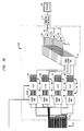
- the video signal generator employs a conventional host processor subsystem 11 which includes a display processor 12, a bulk memory 14, a graphics processor 16, all of which are conventional and well known in the art.
- the video signal generator also utilizes a standard display controller system 18 typically consisting of a standard synchronization module 15 which generates video synchronization signals in response to timing signals, a conventional cursor logic controller 17 and a standard viewport logic controller 19.
- the video signal generator also includes a display generator subsystem 20 which includes a symbol cogenerator 21, a conventional vector/conic cogenerator 23, a standard memory interface unit (MIU) 25, and a conventional area-fill cogenerator 27.
- MIU memory interface unit
- the display generator subsystem 20 generates image data to be displayed on the screen 58 and outputs onto the image bus 22, a standard data/address/command bus structure, including a sixty-four bit signal containing address information of the locations in the bit map memories 36 that the image data is to be written into and also containing color information pertaining to the data to be displayed.
- the image bus 22, which reads or writes in one bus cycle, a sixty four bit word interfaces the display generator subsystem 20 with the refresh memory subsystem 24.
- the refresh memory subsystem 24 is comprised of a plurality of standard bit map memory (BMM) control arrays 34, a plurality of bit map memory arrays 36, and a plurality of bit map memory output multiplexers 38.
- BMM standard bit map memory
- the memory controls' 34 main function is to interface the refresh memory subsystem 24 with the image bus 22 and the video refresh address bus 32.
- the memory controls 34 perform all of the read, write, clear, and data transfer operations based upon the commands it receives from the image buses 22 and the video refresh bus 32.
- the memory controls 34 receive from the image bus 22 the addresses of the BMM arrays 36 where the image data is to be mapped.
- the memory controls 34 transmits an address signal 35, defining the bit map memory array 36 to be addressed and the pixel to be addressed, to the bit map memory arrays 36.
- the bit map memory arrays 36 addresses correspond to addresses of the pixels on the monitor screen 58.
- the address signal 35 received is in the format of 1 x 16 block of pixels along one horizontal raster line or a 4 x 4 block of pixels.
- the arrays 36 are also referred to as bit map memory planes.
- the number of memory planes 36 employed in a raster graphics system is dependent upon the color intensity desired. With ten memory planes 36, each pixel ultimately has ten bits defining its color intensity where one bit is associated with each memory plane 36.
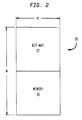
- each of the bit map memory arrays 36 is a N x M array. Since a typical monitor screen 58 requires 2K x 2K of memory, each bit map memory array 36 has enough storage space to store two screens worth of data. Hence, each of the arrays 36 may be defined as one memory plane of 2K x 4K or two pseudo planes 37, 39 each having a size of up to 2K x 2K of storage locations. Initially, the bit map memory address signal 35 carrying image data, is read line by line into the lower plane 39 and once the array 39 is filled, the image data is ready to be displayed on the screen 58.
- the array 39 is toggled so that the array data (video refresh address bus 32), in digital form , is read out of the lower array 39 sixteen bits in parallel (see ref. no. 32). Since one bit represents one pixel, the sixteen bits respectively represent sixteen pixels along one raster line. Data is read out of the array 36 sixteen pixels at a time from each memory plane. While the data is being read out of array 39, the next screen is being formed in the upper plane 37. When the plane 37 is formed, the data stored in the array 37 is read out sixteen pixels in parallel on parallel lines (video refresh address bus 32), while new image data is being formed simultaneously in the lower plane 39 such that the image form/display process flips up back and forth between images being formed in the upper plane 37 and the lower plane 39.
- the ten, sixteen bit array data words (video refresh address bus 32) are input to the bit map memory output multiplexers (MOM) 38 which interface the bit map memory arrays (planes) 36 with the video bus 27.
- MOM's 38 are provided since there is one MOM 38 associated with each memory plane 36.
- the MOM 38 receives the sixteen parallel bit array data word 32 operating at TTL level, and time division multiplexes, in four consecutive clockings, each group of sixteen bits (video refresh address bus 32) into four consecutive four-bit nibbles 26 operating at ECL level. At each clocking, the MOM 38 outputs four bits in parallel, where the four parallel bits define the four-bit nibbles 26.
- Each four-bit nibble 26 represents the color intensity of four of the sixteen pixels, one bit representing one pixel, and each four-bit nibble 26 represents four of the sixteen pixels.
- the nibbles 26 operate at one-fourth of the final pixel frequency rate because instead of processing one sixteen serial bit word output from the bit map memory array, a nibble of one-fourth the length is processed in one-fourth the time.
- a new sixteen bit array data word (video refresh address bus 32) is read out of the bit map memory array 36 and is multiplexed by the MOM 38. Since there are ten MOMs 38, one for each memory plane 36, a total of ten four-bit signals are output from the MOM 38 simultaneously, during one clocking, and carried over the video bus 27.
- the video bus 27 interfaces the MOM's 38 with the video data system 28.
- the video data system 28 is comprised of conventional video multiplexers (video MUX) 401 conventional color look-up tables (CLUT) 46, video output multiplexers (VOM) 50, and conventional digital to analog converters (DAC) 54.
- video MUX video multiplexers
- CLUT color look-up tables
- VOM video output multiplexers
- DAC digital to analog converters
- the video MUX's 40 are arranged and operated in parallel.
- Each of the four bits in the four-bit nibble 26 serves as an input into one of the four video MUX's 40 such that each video MUX 40 receives one bit of data that was output from each of the MOM's 38.
- video MUX 40 is capable of receiving input from up to twenty memory planes and it is capable of outputting data for ten memory planes. Hence, the function of the video MUX 40 is to select which data input is to be output.
- the video MUX 40 receives commands from the display processor 12, instructing it on which of the ten bit map memory planes 36 will be displayed.
- the video MUX 40 outputs a ten parallel bit color intensity code 44, wherein the number of bits in the color code is dependent upon the number of memory planes that will be displayed. Since the illustrated system displays data from ten memory planes 36, the color intensity code 44 is a ten-bit code.
- the ten-bit color intensity code 44 defines the color of a pixel because each of the ten bits represent the color intensity of one pixel on all ten planes 36.
- CLUT 46 There is one CLUT 46 for each video MUX 40 and since the system only employs ten memory planes 36, there is a one for one mapping between the video MUX 40 and the CLUT 46.
- the CLUT 46 provides color information about the pixel location to be displayed on the screen 58.
- Each CLUT 46 is 1K x 16K and the CLUT 46 operates simultaneously in parallel, each table operating on one pixel of data.
- At each address location in the CLUT 46 a fifteen-bit color word is stored.
- the CLUT 46 outputs the fifteen-bit color word, fifteen-bits in parallel 48 and the color word 48 is input into the video output MUX (VOM) 50.
- VOM video output MUX
- the VOMs 50 operate in parallel and each VOM 50 receives one color bit from each of the four fifteen-bit color words 48. Hence, each VOM 50 receives as input a total of four parallel bits 49.
- the VOM 50 functions to perform a four-to-one time division multiplexing on the four-bit input word 49 and outputs one one-bit word, at its final pixel frequency of approximately 400 MHz.
- the fifteen one-bit output 52 from the fifteen video output MUX's 50 forms the final color intensity word for one pixel on the monitor screen 58.
- the VOM 50 has an internal clock and in order to process the original sixteen-bit word 32 four successive clockings are required. At each clocking, the fifteen VOMS 50 which output one bit, cumulatively generate a new fifteen-bit color intensity word, representing the color of one particular pixel.
- the final color intensity word 52 is further arranged into three five-bit words, each five-bit word being designated for each of the three digital to analog converters 54: a red DAC, a green DAC, and a blue DAC.
- the digital to analog convertors 54 convert the fifteen-bit digital color intensity code 52 into a red, green, blue, analog signal 56.
- the analog signal 56 enters a conventional monitor interface 57 which coordinates and synchronizes the signal 57 so that it can be displayed on the monitor screen 58.
- the display monitor screen 58 is updated at periodic intervals every time the display controller system 18 issues a refresh signal 60.
- the viewport logic 19 which is under the control of the sync generator generates the display refresh addresses and signals 60.
- the display refresh addresses and signals 60 are sent to the memory controls 34 which perform the BMM read cycles.
- a refresh signal is received, a new set of sixteen pixels, in the bit map memory array 36, is read out and processed in parallel through the output of the color look-up tables 46 and only at the final output stage of the VOMS 50 will the parallel processing cease and the signals converted to an analog serial bit stream at the final pixel frequency rate.
Landscapes
- Engineering & Computer Science (AREA)
- Physics & Mathematics (AREA)
- Computer Hardware Design (AREA)
- General Physics & Mathematics (AREA)
- Theoretical Computer Science (AREA)
- Radar, Positioning & Navigation (AREA)
- Remote Sensing (AREA)
- Controls And Circuits For Display Device (AREA)
- Transforming Electric Information Into Light Information (AREA)
- Liquid Crystal Display Device Control (AREA)
- Control Of Indicators Other Than Cathode Ray Tubes (AREA)
- Studio Circuits (AREA)
Claims (4)
- Vorrichtung zum Generieren von Videosignalen zur Erzeugung eines Bildes, das durch ehe Vielzahl von Pixeln mit jeweils mehreren Zuständen definiert ist, mit:- einer Vielzahl von Bitkartenspeichern (36) zum Speichern von einer Vielzahl von Datenbits, die jeweils die Zustände der Pixel repräsentieren,- Verarbeitungsmitteln, um gleichzeitig aus den Bitkartenspeichern (36) eine Vielzahl von Datenbits auszulesen, die parallel in den Bitkartenspeichern (36) gespeichert sind,- Tabellenspeichern (46) zum Konvertieren von digitalen Daten in ein Farbwort (48), und- Digital-Analog-Konvertermitteln (54) zum Konvertieren des Farbwortes (48) in die Videosignale,gekennzeichnet durch- eine Vielfalt an die Vielzahl von parallelen Datenbits empfangenden und im Zeitmultiplexverfahren bei einer Frequenz unterhalb von der endgültigen Pixelfrequenz arbeitenden Ausgangsmultiplexern (38) der Bitkartenspeicher, wobei die Ausgabe der Ausgangsmultiplexer (38) der Bitkartenspeicher eine Vielzahl von gemultiplexten Bitgruppen (26) ist, die jeweils eine Anzahl von parallelen Bits umfassen, die geringer ist als die Anzahl der parallelen Datenbits,- wobei die Bitgruppen (26) so in die Tabellenspeicher (46) eingegeben werden, daß jeder Tabellenspeicher (46) ein Bit einer jeden Bitgruppe (26) empfängt,- eine Vielfalt an Videoausgangsmultiplexern (50), wobei die Anzahl der Videoausgangsmultiplexer (50) der Anzahl an Bits in dem Farbwort (48) entspricht und jeder Videoausgangsmultiplexer (50) ein Bit von jedem der Tabellenspeicher (46) empfängt,- wobei die Ausgänge der Videoausgangsmultiplexer (50) mit den Digital-Analog-Konvertern (54) verbunden sind, und- eine Vielzahl an Videomultiplexern (40), die zwischen die Ausgangsmultiplexer (38) der Bitkartenspeicher und die Tabellenspeicher (46) geschaltet sind.
- Vorrichtung nach Anspruch 1, dadurch gekennzeichnet, daß die Bitkartenspeicher (36) die Datenbits an Stellen speichern, die räumlich den Stellen der Pixel in dem Bild entsprechen.
- Vorrichtung nach Anspruch 1 oder 2, dadurch gekennzeichnet, daß wenigstens einer der Bitkartenspeicher (36) genügend Speicherplatz aufweist, um zwei Datenraster zu speichern, die zwei Pseudo-Ebenen (37, 39) entsprechen, wobei Daten in die erste Pseudo-Ebene (37) geschrieben werden, während Daten aus der zweiten Pseudo-Ebene (39) ausgelesen werden.
- Vorrichtung nach einem der vorhergehenden Ansprüche, dadurch gekennzeichnet, daß die Ausgangsmultiplexer (38) der Bitkartenspeicher die Datenbits in TTL-Pegel empfangen und die Bitgruppen (26) mit ECL-Pegel ausgeben.
Applications Claiming Priority (2)
| Application Number | Priority Date | Filing Date | Title |
|---|---|---|---|
| US07/211,492 US4894653A (en) | 1988-06-24 | 1988-06-24 | Method and apparatus for generating video signals |
| US211492 | 1988-06-24 |
Publications (2)
| Publication Number | Publication Date |
|---|---|
| EP0378653A1 EP0378653A1 (de) | 1990-07-25 |
| EP0378653B1 true EP0378653B1 (de) | 1994-03-16 |
Family
ID=22787137
Family Applications (1)
| Application Number | Title | Priority Date | Filing Date |
|---|---|---|---|
| EP89907894A Expired - Lifetime EP0378653B1 (de) | 1988-06-24 | 1989-06-12 | Vorrichtung zur erzeugung von videosignalen |
Country Status (15)
| Country | Link |
|---|---|
| US (1) | US4894653A (de) |
| EP (1) | EP0378653B1 (de) |
| JP (1) | JPH03501300A (de) |
| KR (1) | KR930005367B1 (de) |
| AU (2) | AU3852789A (de) |
| CA (1) | CA1326536C (de) |
| DE (1) | DE68913947T2 (de) |
| DK (1) | DK46990D0 (de) |
| ES (1) | ES2015714A6 (de) |
| IS (1) | IS1435B6 (de) |
| MY (1) | MY105811A (de) |
| NO (1) | NO900400D0 (de) |
| PT (1) | PT90956B (de) |
| TR (1) | TR23908A (de) |
| WO (1) | WO1989012885A1 (de) |
Families Citing this family (16)
| Publication number | Priority date | Publication date | Assignee | Title |
|---|---|---|---|---|
| US5396263A (en) * | 1988-06-13 | 1995-03-07 | Digital Equipment Corporation | Window dependent pixel datatypes in a computer video graphics system |
| US5216413A (en) * | 1988-06-13 | 1993-06-01 | Digital Equipment Corporation | Apparatus and method for specifying windows with priority ordered rectangles in a computer video graphics system |
| US5058041A (en) * | 1988-06-13 | 1991-10-15 | Rose Robert C | Semaphore controlled video chip loading in a computer video graphics system |
| KR910008449B1 (ko) * | 1989-04-04 | 1991-10-15 | 삼성전관 주식회사 | 비데오 매트릭스 회로 |
| GB9013300D0 (en) * | 1990-06-14 | 1990-08-08 | British Aerospace | Video interface circuit |
| US5303321A (en) * | 1990-09-14 | 1994-04-12 | Hughes Aircraft Company | Integrated hardware generator for area fill, conics and vectors in a graphics rendering processor |
| US5255360A (en) * | 1990-09-14 | 1993-10-19 | Hughes Aircraft Company | Dual programmable block texturing and complex clipping in a graphics rendering processor |
| US5276798A (en) * | 1990-09-14 | 1994-01-04 | Hughes Aircraft Company | Multifunction high performance graphics rendering processor |
| WO1992015981A1 (en) * | 1991-03-06 | 1992-09-17 | Analog Devices, Incorporated | Integrated-circuit chip and system for developing timing reference signals for use in high-resolution crt display equipment |
| US5258747A (en) * | 1991-09-30 | 1993-11-02 | Hitachi, Ltd. | Color image displaying system and method thereof |
| US5504503A (en) * | 1993-12-03 | 1996-04-02 | Lsi Logic Corporation | High speed signal conversion method and device |
| US5510843A (en) * | 1994-09-30 | 1996-04-23 | Cirrus Logic, Inc. | Flicker reduction and size adjustment for video controller with interlaced video output |
| US5696534A (en) * | 1995-03-21 | 1997-12-09 | Sun Microsystems Inc. | Time multiplexing pixel frame buffer video output |
| US6456340B1 (en) * | 1998-08-12 | 2002-09-24 | Pixonics, Llc | Apparatus and method for performing image transforms in a digital display system |
| KR100797751B1 (ko) * | 2006-08-04 | 2008-01-23 | 리디스 테크놀로지 인코포레이티드 | 능동 매트릭스 유기 전계 발광 표시 장치의 구동회로 |
| US8363067B1 (en) | 2009-02-05 | 2013-01-29 | Matrox Graphics, Inc. | Processing multiple regions of an image in a graphics display system |
Family Cites Families (18)
| Publication number | Priority date | Publication date | Assignee | Title |
|---|---|---|---|---|
| JPS52149443A (en) * | 1976-06-07 | 1977-12-12 | Japan Radio Co Ltd | System for reading refresh memory |
| US4800380A (en) * | 1982-12-21 | 1989-01-24 | Convergent Technologies | Multi-plane page mode video memory controller |
| JPS60189792A (ja) * | 1984-03-09 | 1985-09-27 | ダイキン工業株式会社 | カラ−crtデイスプレイ装置のカラ−信号発生回路 |
| US4803464A (en) * | 1984-04-16 | 1989-02-07 | Gould Inc. | Analog display circuit including a wideband amplifier circuit for a high resolution raster display system |
| US4673929A (en) * | 1984-04-16 | 1987-06-16 | Gould Inc. | Circuit for processing digital image data in a high resolution raster display system |
| US4724431A (en) * | 1984-09-17 | 1988-02-09 | Honeywell Information Systems Inc. | Computer display system for producing color text and graphics |
| US4704605A (en) * | 1984-12-17 | 1987-11-03 | Edelson Steven D | Method and apparatus for providing anti-aliased edges in pixel-mapped computer graphics |
| JPS61183690A (ja) * | 1985-02-08 | 1986-08-16 | 株式会社東芝 | 画像デイスプレイ装置 |
| US4827255A (en) * | 1985-05-31 | 1989-05-02 | Ascii Corporation | Display control system which produces varying patterns to reduce flickering |
| JPH0731491B2 (ja) * | 1985-07-19 | 1995-04-10 | ヤマハ株式会社 | 画像メモリの読出回路 |
| JPS6228793A (ja) * | 1985-07-31 | 1987-02-06 | 株式会社東芝 | カラ−デイスプレイ装置 |
| JPS6286393A (ja) * | 1985-10-14 | 1987-04-20 | 株式会社日立製作所 | 表示制御装置 |
| JPS62100792A (ja) * | 1985-10-28 | 1987-05-11 | 日本電気株式会社 | 図形表示装置 |
| US4751446A (en) * | 1985-12-06 | 1988-06-14 | Apollo Computer, Inc. | Lookup table initialization |
| US4769632A (en) * | 1986-02-10 | 1988-09-06 | Inmos Limited | Color graphics control system |
| JPS62191886A (ja) * | 1986-02-18 | 1987-08-22 | 住友電気工業株式会社 | 画像表示回路 |
| JPS62280892A (ja) * | 1986-05-30 | 1987-12-05 | 三菱電機株式会社 | モニタテレビ駆動方法 |
| JPS6375790A (ja) * | 1986-09-19 | 1988-04-06 | 株式会社日立製作所 | デイジタル・アナログ変換装置 |
-
1988
- 1988-06-24 US US07/211,492 patent/US4894653A/en not_active Expired - Fee Related
-
1989
- 1989-06-12 JP JP1507341A patent/JPH03501300A/ja active Pending
- 1989-06-12 DE DE68913947T patent/DE68913947T2/de not_active Expired - Lifetime
- 1989-06-12 AU AU38527/89A patent/AU3852789A/en not_active Abandoned
- 1989-06-12 EP EP89907894A patent/EP0378653B1/de not_active Expired - Lifetime
- 1989-06-12 KR KR1019900700378A patent/KR930005367B1/ko not_active Expired - Fee Related
- 1989-06-12 WO PCT/US1989/002550 patent/WO1989012885A1/en not_active Ceased
- 1989-06-15 MY MYPI89000803A patent/MY105811A/en unknown
- 1989-06-21 ES ES8902160A patent/ES2015714A6/es not_active Expired - Fee Related
- 1989-06-21 CA CA000603516A patent/CA1326536C/en not_active Expired - Fee Related
- 1989-06-22 TR TR65089A patent/TR23908A/xx unknown
- 1989-06-22 IS IS3481A patent/IS1435B6/is unknown
- 1989-06-23 PT PT90956A patent/PT90956B/pt not_active IP Right Cessation
-
1990
- 1990-01-29 NO NO900400A patent/NO900400D0/no unknown
- 1990-02-22 DK DK046990A patent/DK46990D0/da not_active Application Discontinuation
-
1992
- 1992-06-05 AU AU18061/92A patent/AU650139B2/en not_active Ceased
Also Published As
| Publication number | Publication date |
|---|---|
| WO1989012885A1 (en) | 1989-12-28 |
| PT90956A (pt) | 1989-12-29 |
| MY105811A (en) | 1995-01-30 |
| KR930005367B1 (ko) | 1993-06-19 |
| EP0378653A1 (de) | 1990-07-25 |
| KR900702499A (ko) | 1990-12-07 |
| DE68913947T2 (de) | 1994-07-07 |
| TR23908A (tr) | 1990-11-05 |
| US4894653A (en) | 1990-01-16 |
| DK46990A (da) | 1990-02-22 |
| CA1326536C (en) | 1994-01-25 |
| NO900400L (no) | 1990-01-29 |
| NO900400D0 (no) | 1990-01-29 |
| ES2015714A6 (es) | 1990-09-01 |
| IS1435B6 (is) | 1990-07-16 |
| AU650139B2 (en) | 1994-06-09 |
| DK46990D0 (da) | 1990-02-22 |
| JPH03501300A (ja) | 1991-03-22 |
| AU1806192A (en) | 1992-07-30 |
| AU3852789A (en) | 1990-01-12 |
| IS3481A7 (is) | 1989-12-25 |
| DE68913947D1 (de) | 1994-04-21 |
| PT90956B (pt) | 1994-09-30 |
Similar Documents
| Publication | Publication Date | Title |
|---|---|---|
| EP0378653B1 (de) | Vorrichtung zur erzeugung von videosignalen | |
| KR100274838B1 (ko) | 공간 광 변조기 디스플레이 시스템을 제어하는 방법 및 시스템 제어기 | |
| EP0071725B1 (de) | Verfahren zur Verschiebung von Texten und grafischen Daten in selektierte Bildfenster auf einer graphischen Darstellung | |
| EP0524468B1 (de) | Hochauflösende Multimediaanzeige | |
| US4823120A (en) | Enhanced video graphics controller | |
| US5247612A (en) | Pixel display apparatus and method using a first-in, first-out buffer | |
| WO1990002991A1 (en) | Graphics processor with staggered memory timing | |
| US5268682A (en) | Resolution independent raster display system | |
| GB2104354A (en) | Writing text characters on computer graphics display | |
| EP0139093A2 (de) | Rasteranzeigesystem mit mehreren Speichern | |
| KR100384348B1 (ko) | 영상데이타처리방법 | |
| EP0139095A2 (de) | Bildauswahl in einem Rasteranzeigesystem | |
| US5086295A (en) | Apparatus for increasing color and spatial resolutions of a raster graphics system | |
| US5230064A (en) | High resolution graphic display organization | |
| GB2151440A (en) | A circuit for increasing the number of pixels in a scan of a bit mapping type video display | |
| KR900006942B1 (ko) | 데이타 디스플레이 시스템용 데이타 신호 제공 장치 | |
| US5097256A (en) | Method of generating a cursor | |
| EP0283579B1 (de) | Nach dem Rasterverfahren arbeitendes Anzeigesystem mit einem einen Randomspeicher enthaltenden Zeichengenerator | |
| JPH08179740A (ja) | 画像データ伝送方法および画像表示装置 | |
| JP3241769B2 (ja) | ラスター表示装置 | |
| JPS58105189A (ja) | 表示メモリの制御装置 | |
| JPH05265415A (ja) | 画像表示制御回路 | |
| JPS61251283A (ja) | 静止画送信装置 | |
| JPS5923388A (ja) | 色表示制御装置 | |
| JPS63127287A (ja) | カ−ソル表示方式 |
Legal Events
| Date | Code | Title | Description |
|---|---|---|---|
| PUAI | Public reference made under article 153(3) epc to a published international application that has entered the european phase |
Free format text: ORIGINAL CODE: 0009012 |
|
| 17P | Request for examination filed |
Effective date: 19900215 |
|
| AK | Designated contracting states |
Kind code of ref document: A1 Designated state(s): BE CH DE FR GB IT LI NL SE |
|
| 17Q | First examination report despatched |
Effective date: 19920703 |
|
| GRAA | (expected) grant |
Free format text: ORIGINAL CODE: 0009210 |
|
| ITF | It: translation for a ep patent filed | ||
| AK | Designated contracting states |
Kind code of ref document: B1 Designated state(s): BE CH DE FR GB IT LI NL SE |
|
| REF | Corresponds to: |
Ref document number: 68913947 Country of ref document: DE Date of ref document: 19940421 |
|
| ET | Fr: translation filed | ||
| PLBE | No opposition filed within time limit |
Free format text: ORIGINAL CODE: 0009261 |
|
| STAA | Information on the status of an ep patent application or granted ep patent |
Free format text: STATUS: NO OPPOSITION FILED WITHIN TIME LIMIT |
|
| EAL | Se: european patent in force in sweden |
Ref document number: 89907894.3 |
|
| 26N | No opposition filed | ||
| REG | Reference to a national code |
Ref country code: GB Ref legal event code: 732E |
|
| REG | Reference to a national code |
Ref country code: FR Ref legal event code: TP Ref country code: FR Ref legal event code: CD Ref country code: FR Ref legal event code: CA |
|
| PGFP | Annual fee paid to national office [announced via postgrant information from national office to epo] |
Ref country code: SE Payment date: 20000519 Year of fee payment: 12 |
|
| PGFP | Annual fee paid to national office [announced via postgrant information from national office to epo] |
Ref country code: CH Payment date: 20000522 Year of fee payment: 12 |
|
| PGFP | Annual fee paid to national office [announced via postgrant information from national office to epo] |
Ref country code: NL Payment date: 20000524 Year of fee payment: 12 |
|
| PGFP | Annual fee paid to national office [announced via postgrant information from national office to epo] |
Ref country code: BE Payment date: 20000615 Year of fee payment: 12 |
|
| PG25 | Lapsed in a contracting state [announced via postgrant information from national office to epo] |
Ref country code: SE Free format text: LAPSE BECAUSE OF NON-PAYMENT OF DUE FEES Effective date: 20010613 |
|
| PG25 | Lapsed in a contracting state [announced via postgrant information from national office to epo] |
Ref country code: CH Free format text: LAPSE BECAUSE OF NON-PAYMENT OF DUE FEES Effective date: 20010630 Ref country code: BE Free format text: LAPSE BECAUSE OF NON-PAYMENT OF DUE FEES Effective date: 20010630 Ref country code: LI Free format text: LAPSE BECAUSE OF NON-PAYMENT OF DUE FEES Effective date: 20010630 |
|
| NLS | Nl: assignments of ep-patents |
Owner name: RAYTHEON COMPANY;HE HOLDINGS, INC. |
|
| BERE | Be: lapsed |
Owner name: HUGHES AIRCRAFT CY Effective date: 20010630 |
|
| PG25 | Lapsed in a contracting state [announced via postgrant information from national office to epo] |
Ref country code: NL Free format text: LAPSE BECAUSE OF NON-PAYMENT OF DUE FEES Effective date: 20020101 |
|
| REG | Reference to a national code |
Ref country code: GB Ref legal event code: IF02 |
|
| EUG | Se: european patent has lapsed |
Ref document number: 89907894.3 |
|
| REG | Reference to a national code |
Ref country code: CH Ref legal event code: PL |
|
| NLV4 | Nl: lapsed or anulled due to non-payment of the annual fee |
Effective date: 20020101 |
|
| PG25 | Lapsed in a contracting state [announced via postgrant information from national office to epo] |
Ref country code: IT Free format text: LAPSE BECAUSE OF NON-PAYMENT OF DUE FEES;WARNING: LAPSES OF ITALIAN PATENTS WITH EFFECTIVE DATE BEFORE 2007 MAY HAVE OCCURRED AT ANY TIME BEFORE 2007. THE CORRECT EFFECTIVE DATE MAY BE DIFFERENT FROM THE ONE RECORDED. Effective date: 20050612 |
|
| PGFP | Annual fee paid to national office [announced via postgrant information from national office to epo] |
Ref country code: DE Payment date: 20080523 Year of fee payment: 20 |
|
| PGFP | Annual fee paid to national office [announced via postgrant information from national office to epo] |
Ref country code: GB Payment date: 20080521 Year of fee payment: 20 |
|
| REG | Reference to a national code |
Ref country code: GB Ref legal event code: PE20 Expiry date: 20090611 |
|
| PG25 | Lapsed in a contracting state [announced via postgrant information from national office to epo] |
Ref country code: GB Free format text: LAPSE BECAUSE OF EXPIRATION OF PROTECTION Effective date: 20090611 |
|
| PGFP | Annual fee paid to national office [announced via postgrant information from national office to epo] |
Ref country code: FR Payment date: 20080513 Year of fee payment: 20 |