EP0379024A2 - Méthode de fabrication d'un élément semi-conducteur - Google Patents
Méthode de fabrication d'un élément semi-conducteur Download PDFInfo
- Publication number
- EP0379024A2 EP0379024A2 EP90100301A EP90100301A EP0379024A2 EP 0379024 A2 EP0379024 A2 EP 0379024A2 EP 90100301 A EP90100301 A EP 90100301A EP 90100301 A EP90100301 A EP 90100301A EP 0379024 A2 EP0379024 A2 EP 0379024A2
- Authority
- EP
- European Patent Office
- Prior art keywords
- layer
- manufacturing
- gate
- polysilicon layer
- substrate
- Prior art date
- Legal status (The legal status is an assumption and is not a legal conclusion. Google has not performed a legal analysis and makes no representation as to the accuracy of the status listed.)
- Granted
Links
Images



Classifications
-
- H—ELECTRICITY
- H10—SEMICONDUCTOR DEVICES; ELECTRIC SOLID-STATE DEVICES NOT OTHERWISE PROVIDED FOR
- H10D—INORGANIC ELECTRIC SEMICONDUCTOR DEVICES
- H10D64/00—Electrodes of devices having potential barriers
- H10D64/60—Electrodes characterised by their materials
- H10D64/66—Electrodes having a conductor capacitively coupled to a semiconductor by an insulator, e.g. MIS electrodes
- H10D64/661—Electrodes having a conductor capacitively coupled to a semiconductor by an insulator, e.g. MIS electrodes the conductor comprising a layer of silicon contacting the insulator, e.g. polysilicon having vertical doping variation
- H10D64/662—Electrodes having a conductor capacitively coupled to a semiconductor by an insulator, e.g. MIS electrodes the conductor comprising a layer of silicon contacting the insulator, e.g. polysilicon having vertical doping variation the conductor further comprising additional layers, e.g. multiple silicon layers having different crystal structures
- H10D64/663—Electrodes having a conductor capacitively coupled to a semiconductor by an insulator, e.g. MIS electrodes the conductor comprising a layer of silicon contacting the insulator, e.g. polysilicon having vertical doping variation the conductor further comprising additional layers, e.g. multiple silicon layers having different crystal structures the additional layers comprising a silicide layer contacting the layer of silicon, e.g. polycide gates
-
- H—ELECTRICITY
- H10—SEMICONDUCTOR DEVICES; ELECTRIC SOLID-STATE DEVICES NOT OTHERWISE PROVIDED FOR
- H10D—INORGANIC ELECTRIC SEMICONDUCTOR DEVICES
- H10D30/00—Field-effect transistors [FET]
- H10D30/01—Manufacture or treatment
- H10D30/021—Manufacture or treatment of FETs having insulated gates [IGFET]
- H10D30/0223—Manufacture or treatment of FETs having insulated gates [IGFET] having source and drain regions or source and drain extensions self-aligned to sides of the gate
-
- H—ELECTRICITY
- H10—SEMICONDUCTOR DEVICES; ELECTRIC SOLID-STATE DEVICES NOT OTHERWISE PROVIDED FOR
- H10P—GENERIC PROCESSES OR APPARATUS FOR THE MANUFACTURE OR TREATMENT OF DEVICES COVERED BY CLASS H10
- H10P30/00—Ion implantation into wafers, substrates or parts of devices
- H10P30/20—Ion implantation into wafers, substrates or parts of devices into semiconductor materials, e.g. for doping
-
- Y—GENERAL TAGGING OF NEW TECHNOLOGICAL DEVELOPMENTS; GENERAL TAGGING OF CROSS-SECTIONAL TECHNOLOGIES SPANNING OVER SEVERAL SECTIONS OF THE IPC; TECHNICAL SUBJECTS COVERED BY FORMER USPC CROSS-REFERENCE ART COLLECTIONS [XRACs] AND DIGESTS
- Y10—TECHNICAL SUBJECTS COVERED BY FORMER USPC
- Y10S—TECHNICAL SUBJECTS COVERED BY FORMER USPC CROSS-REFERENCE ART COLLECTIONS [XRACs] AND DIGESTS
- Y10S148/00—Metal treatment
- Y10S148/019—Contacts of silicides
-
- Y—GENERAL TAGGING OF NEW TECHNOLOGICAL DEVELOPMENTS; GENERAL TAGGING OF CROSS-SECTIONAL TECHNOLOGIES SPANNING OVER SEVERAL SECTIONS OF THE IPC; TECHNICAL SUBJECTS COVERED BY FORMER USPC CROSS-REFERENCE ART COLLECTIONS [XRACs] AND DIGESTS
- Y10—TECHNICAL SUBJECTS COVERED BY FORMER USPC
- Y10S—TECHNICAL SUBJECTS COVERED BY FORMER USPC CROSS-REFERENCE ART COLLECTIONS [XRACs] AND DIGESTS
- Y10S148/00—Metal treatment
- Y10S148/147—Silicides
-
- Y—GENERAL TAGGING OF NEW TECHNOLOGICAL DEVELOPMENTS; GENERAL TAGGING OF CROSS-SECTIONAL TECHNOLOGIES SPANNING OVER SEVERAL SECTIONS OF THE IPC; TECHNICAL SUBJECTS COVERED BY FORMER USPC CROSS-REFERENCE ART COLLECTIONS [XRACs] AND DIGESTS
- Y10—TECHNICAL SUBJECTS COVERED BY FORMER USPC
- Y10S—TECHNICAL SUBJECTS COVERED BY FORMER USPC CROSS-REFERENCE ART COLLECTIONS [XRACs] AND DIGESTS
- Y10S438/00—Semiconductor device manufacturing: process
- Y10S438/91—Controlling charging state at semiconductor-insulator interface
Definitions
- This invention relates to a method for manufacturing semiconductor devices of polycide gate structure, and more particularly to a method used for manufacturing semiconductor devices having a thin gate oxide film.
- semiconductor impurity is ion-implanted into a semiconductor substrate to form source and drain regions.
- charges caused by the ion-implantation are injected into the gate electrode so as to charge the gate electrode (gate charge).
- the gate charging increases the potential of the gate electrode so that the gate oxide film may be subject to dielectric breakdown by the electric field created between the substrate and the gate electrode when the gate oxide film is thin.
- the ion-implantation is generally effected with the gate electrode layer and the silicon substrate held in contact with each other. With the gate electrode layer kept in contact with the silicon substrate, charges caused by the ion-implantation will not be stored in the gate electrode but discharged into the substrate.
- the gate electrode layer In order to set the gate electrode layer in contact with the silicon substrate, it is necessary to remove the contact portion of the gate electrode layer by the photolithographic process, for example, and form a contact hole for connection with the gate oxide film.
- a photoresist film of a predetermined pattern is formed on the thin gate oxide film and the gate oxide film is selectively etched to form the contact hole using the resist film as a mask.
- formation of the photoresist layer on the thin gate oxide film may significantly degrade the quality of the surface of the gate oxide film and increase the weak-point density.
- material mixed into the photoresist layer may be injected into the gate oxide film to lower the electrical stability of the gate oxide film.
- This invention has been made in view of the above fact and an object of this invention is to provide a semiconductor device manufacturing method capable of suppressing the gate charge at the time of ion-implantation and preventing occurrence of damage to the gate oxide film in the manufacturing process and injection of unwanted material into the gate oxide film.
- the semiconductor device manufacturing method of this invention comprises the steps of forming a gate insulation film on a semiconductor substrate; and forming a polysilicon layer on the gate insulation film.
- the polysilicon layer and the gate insulation film are selectively removed on form an opening which reaches the semiconductor substrate in the polysilicon layer and the gate insulation film.
- a silicide film is formed directly on the polysilicon layer and an exposed part of the semiconductor substrate and then ion-implantation is effected to form source and drain regions.
- the silicide film is formed in direct contact with the semiconductor substrate, charges caused by the ion-implantation can be easily discharged into the semiconductor substrate. Therefore, no gate charge will occur. Further, the gate oxide film is prevented from being brought into contact with the photoresist layer by the presence of the polysilicon layer. Therefore, damage of the surface of the gate oxide film due to the direct contact with the photoresist layer will not occur and unwanted material may be prevented from being injected from the photoresist layer into the gate oxide film.
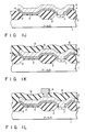
- Figs. 1A to 1L are cross sectional views of semiconductor structures in respective steps of a manufacturing method according to one embodiment of this invention.
- Figs. 2A to 2C are cross sectional views of semiconductor structures in respective manufacturing steps in a modification of the embodiment explained with reference to Figs. 1A to 1L.
- This embodiment is made by applying the manufacturing method of this invention to a method for manufacturing a semiconductor device having transistor elements.
- Figs. 1A to 1L are cross sectional views of semiconductor structures in respective steps of a manufacturing method according to the embodiment of this invention.
- the cross sectional views show the cross sections taken along lines extending in the lengthwise direction of the gate electrode of the transistor element and therefore the source and drain regions are not shown.
- an element isolation region (SiO2 region) 2 is formed in a p-type silicon substrate 1 by the thermal oxidation method.
- a gate oxide film Part of the oxide film 3 which lies on the transistor region 21 constitutes a gate oxide film.
- a polysilicon layer 4 is formed by the CVD method to a thickness of approx. 1500 ⁇ .
- n-typr impurity such as As+ is ion-implanted into the polysilicon layer 4 to enhance the electrical conductivity thereof.
- phosphorus may be diffused into the polysilicon layer 4.
- As+ ion-implantation performed during this step a charge-up will not occur in the polysilicon layer 4, since the polysilicon layer 4 is generally connected to the ground during the ion-implantation step via the conductive wafer-holder (not shown) of an ion-implanting device (not shown), for holding the semiconductor wafer (the semiconductor structure), the wafer-holder generally being grounded.
- a photoresist layer 5 is formed on the polysilicon layer 4 and then patterned to form an opening in the contact area.
- the polysilicon layer 4 and the gate oxide film 3 are selectively etched to form an opening 11 which reaches the substrate 1 in the contact area 22 as shown in Fig. 1F.
- a metal silicide layer such as a tungsten silicide (WSi) layer 6 is formed to a thickness of approx. 3000 ⁇ by the CVD method.
- the silicide layer 6 is formed to extend into the opening 11 so as to be made in contact with the exposed portion of the substrate.
- the metal silicide layer and polysilicon layer 4 are patterned to form a polycide gate electrode 12 of a predetermined pattern.
- Fig. 1I for example, As+ is ion-implanted to an impurity density of 1 ⁇ 1015 cm ⁇ 2, for example, as an n-type impurity source used for forming source and drain regions (as described before, since the cross sections are taken along lines extending in the lengthwise direction of the transistor element and therefore the source and drain regions are not shown. In the drawing, the source and drain regions lie behind and before the paper in the transistor region 21). Since the silicide layer 6 is formed in direct contact with the substrate 1, charges caused by the ion-implantation are discharged into the substrate via the silicide layer 6. As a result, almost no charge is stored in the gate electrode layer 12. That is, substantially no gate charge occurs.
- the heat treatment is effected to activate implanted As+ so as to form source and drain regions.
- As+ implanted into the silicide layer 6 is diffused into the substrate 1 via the contact area between the silicide layer 6 and the substrate 1 to form an n-type diffusion layer 7 in in that part of the substrate 1 which corresponds to the contact area 22 as shown in Fig. 1J.
- a metal layer 9 of aluminum is formed on the entire surface of the resultant structure by the sputtering method and is patterned to form a gate electrode lead-out layer 9.
- the silicide layer 6 is formed in direct contact with the substrate 1 so that charges caused by the ion-implantation may be discharged via the substrate. As a result, unwanted gate charge will not occur.
- the polysilicon layer 4 is formed between the gate oxide film 3 and photoresist layer 5 and thus the gate oxide film 3 is not formed in direct contact with the resist layer. Therefore, occurrence of damage to the surface area of the gate oxide film 3 caused when the resist layer 5 is formed in direct contact with the gate oxide film 3 can be prevented and injection of unwanted material from the resist layer into the gate oxide film can also be prevented.
- portions of the silicide layer 6 and the polysilicon layer 4 which lie on the element isolation region 2 between the transistor region 21 and the contact area 22 are etched out to isolate an area of the electrode layer 22 acting as the gate electrode from the substrate 1 as shown in Fig. 2A.
- the operation voltage of this device will not be limited by the withstanding voltage of the pn junction.
- an interlayer insulation film 8 of SiO2, for example, is formed on the entire surface of the resultant structure by the CVD method and is patterned to form an opening which reaches the silicide layer 6.
- a metal layer 9 of aluminum is formed on the entire surface of the resultant structure by the sputtering method and is patterned to form a gate electrode lead-out layer 9.
- the manufacturing method of this invention is used for manufacturing semiconductor devices in which a gate electrode is formed as a continuous layer extending over a plurality of memory cells.
- a single-layered gate structure is used.
- a two-layered or multi-layered gate structure can be applied in this invention.
- the gate electrode layer is formed with the polycide gate structure of the polysilicon layer and WSi layer.
- the silicide layer is not limited to the WSi layer but a MoSi, TiSi layer or the like can be used as the silicide layer.
- the deposition method of the silicide layer is not limited to the CVD method, and the sputtering method or the like can be used.
- n-type silicon substrate instead of the p-type silicon substrate.
- p-type impurity such as boron (B) as the impurity to be implanted instead of the n-type impurity.
Landscapes
- Insulated Gate Type Field-Effect Transistor (AREA)
- Electrodes Of Semiconductors (AREA)
Applications Claiming Priority (2)
| Application Number | Priority Date | Filing Date | Title |
|---|---|---|---|
| JP11624/89 | 1989-01-20 | ||
| JP1011624A JPH0724261B2 (ja) | 1989-01-20 | 1989-01-20 | 半導体装置の製造方法 |
Publications (3)
| Publication Number | Publication Date |
|---|---|
| EP0379024A2 true EP0379024A2 (fr) | 1990-07-25 |
| EP0379024A3 EP0379024A3 (fr) | 1990-08-29 |
| EP0379024B1 EP0379024B1 (fr) | 1997-11-19 |
Family
ID=11783081
Family Applications (1)
| Application Number | Title | Priority Date | Filing Date |
|---|---|---|---|
| EP90100301A Expired - Lifetime EP0379024B1 (fr) | 1989-01-20 | 1990-01-08 | Méthode de fabrication d'un élément semi-conducteur |
Country Status (5)
| Country | Link |
|---|---|
| US (1) | US5049514A (fr) |
| EP (1) | EP0379024B1 (fr) |
| JP (1) | JPH0724261B2 (fr) |
| KR (1) | KR930004117B1 (fr) |
| DE (1) | DE69031712T2 (fr) |
Cited By (2)
| Publication number | Priority date | Publication date | Assignee | Title |
|---|---|---|---|---|
| EP0601652A3 (fr) * | 1992-12-11 | 1998-02-25 | Philips Electronics Uk Limited | Fabrication d'un dispositif électronique utilisant une implantation ionique |
| EP0903789A3 (fr) * | 1997-09-19 | 1999-12-08 | Nec Corporation | Dispositif semi-conducteur de mémoire rémanente et procédé pour sa fabrication |
Families Citing this family (15)
| Publication number | Priority date | Publication date | Assignee | Title |
|---|---|---|---|---|
| JP2892421B2 (ja) * | 1990-02-27 | 1999-05-17 | 沖電気工業株式会社 | 半導体素子の製造方法 |
| EP0575280A3 (en) * | 1992-06-18 | 1995-10-04 | Ibm | Cmos transistor with two-layer inverse-t tungsten gate structure |
| US5326713A (en) * | 1992-09-04 | 1994-07-05 | Taiwan Semiconductor Manufacturies Company | Buried contact process |
| US5272099A (en) * | 1992-11-27 | 1993-12-21 | Etron Technology Inc. | Fabrication of transistor contacts |
| US5393687A (en) * | 1993-12-16 | 1995-02-28 | Taiwan Semiconductor Manufacturing Company | Method of making buried contact module with multiple poly si layers |
| JP2924622B2 (ja) * | 1993-12-28 | 1999-07-26 | 日本電気株式会社 | 半導体装置の製造方法 |
| US5767006A (en) * | 1996-09-27 | 1998-06-16 | Taiwan Semiconductor Manufacturating Company, Ltd. | Method for eliminating charge damage during etching of conducting layers |
| US5866482A (en) * | 1996-09-27 | 1999-02-02 | Taiwan Semiconductor Manufacturing Company, Ltd. | Method for masking conducting layers to abate charge damage during plasma etching |
| US6020237A (en) * | 1998-02-04 | 2000-02-01 | Alliance Semiconductor Corporation | Method of reducing dielectric damage due to charging in the fabrication of stacked gate structures |
| DE10201058A1 (de) * | 2002-01-14 | 2003-07-31 | Infineon Technologies Ag | Verfahren zur Herstellung einer dielektrischen Schicht |
| JP3481233B1 (ja) | 2002-05-27 | 2003-12-22 | 沖電気工業株式会社 | キャパシタ構造の製造方法及びキャパシタ素子の製造方法 |
| JP4454921B2 (ja) * | 2002-09-27 | 2010-04-21 | 株式会社半導体エネルギー研究所 | 半導体装置の作製方法 |
| JP4683817B2 (ja) * | 2002-09-27 | 2011-05-18 | 株式会社半導体エネルギー研究所 | 半導体装置の作製方法 |
| US7118959B2 (en) * | 2005-03-10 | 2006-10-10 | Texas Instruments Incorporated | Integrated circuit capacitor having antireflective dielectric |
| RU2751983C1 (ru) * | 2020-11-20 | 2021-07-21 | Федеральное государственное бюджетное образовательное учреждение высшего образования "Кабардино-Балкарский государственный университет им. Х.М. Бербекова" (КБГУ) | Способ изготовления силицида титана |
Family Cites Families (8)
| Publication number | Priority date | Publication date | Assignee | Title |
|---|---|---|---|---|
| US4224733A (en) * | 1977-10-11 | 1980-09-30 | Fujitsu Limited | Ion implantation method |
| JPS57100768A (en) * | 1980-12-16 | 1982-06-23 | Nec Corp | Manufacture of field effect semiconductor device |
| US4551908A (en) * | 1981-06-15 | 1985-11-12 | Nippon Electric Co., Ltd. | Process of forming electrodes and interconnections on silicon semiconductor devices |
| US4558507A (en) * | 1982-11-12 | 1985-12-17 | Nec Corporation | Method of manufacturing semiconductor device |
| US4740479A (en) * | 1985-07-05 | 1988-04-26 | Siemens Aktiengesellschaft | Method for the manufacture of cross-couplings between n-channel and p-channel CMOS field effect transistors of static write-read memories |
| WO1987000967A1 (fr) * | 1985-08-08 | 1987-02-12 | Motorola, Inc. | Technique de prevention de la rupture dielectrique |
| US4788160A (en) * | 1987-03-31 | 1988-11-29 | Texas Instruments Incorporated | Process for formation of shallow silicided junctions |
| US4859278A (en) * | 1988-08-11 | 1989-08-22 | Xerox Corporation | Fabrication of high resistive loads utilizing a single level polycide process |
-
1989
- 1989-01-20 JP JP1011624A patent/JPH0724261B2/ja not_active Expired - Fee Related
- 1989-12-22 KR KR1019890019285A patent/KR930004117B1/ko not_active Expired - Fee Related
-
1990
- 1990-01-08 DE DE69031712T patent/DE69031712T2/de not_active Expired - Fee Related
- 1990-01-08 EP EP90100301A patent/EP0379024B1/fr not_active Expired - Lifetime
- 1990-01-18 US US07/466,924 patent/US5049514A/en not_active Expired - Lifetime
Cited By (4)
| Publication number | Priority date | Publication date | Assignee | Title |
|---|---|---|---|---|
| EP0601652A3 (fr) * | 1992-12-11 | 1998-02-25 | Philips Electronics Uk Limited | Fabrication d'un dispositif électronique utilisant une implantation ionique |
| EP0903789A3 (fr) * | 1997-09-19 | 1999-12-08 | Nec Corporation | Dispositif semi-conducteur de mémoire rémanente et procédé pour sa fabrication |
| US6392268B2 (en) | 1997-09-19 | 2002-05-21 | Nec Corporation | Nonvolatile semiconductor storage apparatus and production method of the same |
| US6503797B2 (en) | 1997-09-19 | 2003-01-07 | Nec Corporation | Nonvolatile semiconductor storage apparatus and production method of the same |
Also Published As
| Publication number | Publication date |
|---|---|
| KR900012331A (ko) | 1990-08-03 |
| DE69031712T2 (de) | 1998-04-09 |
| DE69031712D1 (de) | 1998-01-02 |
| EP0379024A3 (fr) | 1990-08-29 |
| US5049514A (en) | 1991-09-17 |
| JPH0724261B2 (ja) | 1995-03-15 |
| KR930004117B1 (ko) | 1993-05-20 |
| EP0379024B1 (fr) | 1997-11-19 |
| JPH02192723A (ja) | 1990-07-30 |
Similar Documents
| Publication | Publication Date | Title |
|---|---|---|
| US6524893B2 (en) | Electrostatic discharge protection device for semiconductor integrated circuit, method for producing the same, and electrostatic discharge protection circuit using the same | |
| US4319395A (en) | Method of making self-aligned device | |
| US6004838A (en) | ESD protection using selective siliciding techniques | |
| EP0379024A2 (fr) | Méthode de fabrication d'un élément semi-conducteur | |
| US6869840B2 (en) | Compensated-well electrostatic discharge protection devices | |
| US5395787A (en) | Method of manufacturing shallow junction field effect transistor | |
| US5953601A (en) | ESD implantation scheme for 0.35 μm 3.3V 70A gate oxide process | |
| EP0749158B1 (fr) | Procédé pour la fabrication d'un dispositif semi-conducteur avec grille auto-alignée en polycide | |
| US5328860A (en) | Method of manufacturing a semiconductor device | |
| EP0656645B1 (fr) | Transistor à effet de champ à jonction diffusée scellée | |
| JP3141446B2 (ja) | 半導体装置の製造方法 | |
| JP2723221B2 (ja) | 半導体装置の製造方法 | |
| US5225896A (en) | Protection element and method of manufacturing same | |
| JP3398077B2 (ja) | 半導体装置及びその製造方法 | |
| KR100224757B1 (ko) | 반도체 장치 및 그 제조방법 | |
| EP0381280B1 (fr) | Procédé de fabrication d'un circuit intégré avec un élément de protection | |
| JP3212882B2 (ja) | 半導体装置の製造方法 | |
| KR100275946B1 (ko) | 반도체장치의이에스디회로제조방법 | |
| KR100269613B1 (ko) | 반도체장치의 제조방법 | |
| KR100249016B1 (ko) | 반도체장치의 이에스디 보호회로 제조방법 | |
| JPH04348039A (ja) | 半導体装置の製造方法 | |
| KR20000039155A (ko) | 정전방전 방지 트랜지스터 및 그 제조방법 | |
| JPH10163490A (ja) | トランジスタの製造方法 | |
| JPH0521376A (ja) | 半導体装置の製造方法 | |
| KR19980025487A (ko) | 바이폴라 트랜지스터의 제조방법 |
Legal Events
| Date | Code | Title | Description |
|---|---|---|---|
| PUAI | Public reference made under article 153(3) epc to a published international application that has entered the european phase |
Free format text: ORIGINAL CODE: 0009012 |
|
| PUAL | Search report despatched |
Free format text: ORIGINAL CODE: 0009013 |
|
| 17P | Request for examination filed |
Effective date: 19900108 |
|
| AK | Designated contracting states |
Kind code of ref document: A2 Designated state(s): DE FR GB |
|
| AK | Designated contracting states |
Kind code of ref document: A3 Designated state(s): DE FR GB |
|
| 17Q | First examination report despatched |
Effective date: 19930225 |
|
| GRAG | Despatch of communication of intention to grant |
Free format text: ORIGINAL CODE: EPIDOS AGRA |
|
| GRAH | Despatch of communication of intention to grant a patent |
Free format text: ORIGINAL CODE: EPIDOS IGRA |
|
| GRAH | Despatch of communication of intention to grant a patent |
Free format text: ORIGINAL CODE: EPIDOS IGRA |
|
| GRAA | (expected) grant |
Free format text: ORIGINAL CODE: 0009210 |
|
| RAP1 | Party data changed (applicant data changed or rights of an application transferred) |
Owner name: KABUSHIKI KAISHA TOSHIBA |
|
| AK | Designated contracting states |
Kind code of ref document: B1 Designated state(s): DE FR GB |
|
| PGFP | Annual fee paid to national office [announced via postgrant information from national office to epo] |
Ref country code: GB Payment date: 19971230 Year of fee payment: 9 |
|
| REF | Corresponds to: |
Ref document number: 69031712 Country of ref document: DE Date of ref document: 19980102 |
|
| PGFP | Annual fee paid to national office [announced via postgrant information from national office to epo] |
Ref country code: DE Payment date: 19980116 Year of fee payment: 9 |
|
| ET | Fr: translation filed | ||
| PLBE | No opposition filed within time limit |
Free format text: ORIGINAL CODE: 0009261 |
|
| STAA | Information on the status of an ep patent application or granted ep patent |
Free format text: STATUS: NO OPPOSITION FILED WITHIN TIME LIMIT |
|
| 26N | No opposition filed | ||
| PG25 | Lapsed in a contracting state [announced via postgrant information from national office to epo] |
Ref country code: GB Free format text: LAPSE BECAUSE OF NON-PAYMENT OF DUE FEES Effective date: 19990108 |
|
| REG | Reference to a national code |
Ref country code: FR Ref legal event code: D6 |
|
| GBPC | Gb: european patent ceased through non-payment of renewal fee |
Effective date: 19990108 |
|
| PG25 | Lapsed in a contracting state [announced via postgrant information from national office to epo] |
Ref country code: DE Free format text: LAPSE BECAUSE OF NON-PAYMENT OF DUE FEES Effective date: 19991103 |
|
| PGFP | Annual fee paid to national office [announced via postgrant information from national office to epo] |
Ref country code: FR Payment date: 20060110 Year of fee payment: 17 |
|
| REG | Reference to a national code |
Ref country code: FR Ref legal event code: ST Effective date: 20070930 |
|
| PG25 | Lapsed in a contracting state [announced via postgrant information from national office to epo] |
Ref country code: FR Free format text: LAPSE BECAUSE OF NON-PAYMENT OF DUE FEES Effective date: 20070131 |