EP0380138A2 - Méthode de fabrication d'un guide d'ondes - Google Patents
Méthode de fabrication d'un guide d'ondes Download PDFInfo
- Publication number
- EP0380138A2 EP0380138A2 EP90101626A EP90101626A EP0380138A2 EP 0380138 A2 EP0380138 A2 EP 0380138A2 EP 90101626 A EP90101626 A EP 90101626A EP 90101626 A EP90101626 A EP 90101626A EP 0380138 A2 EP0380138 A2 EP 0380138A2
- Authority
- EP
- European Patent Office
- Prior art keywords
- substrate
- implanted
- optical waveguide
- ions
- ionic species
- Prior art date
- Legal status (The legal status is an assumption and is not a legal conclusion. Google has not performed a legal analysis and makes no representation as to the accuracy of the status listed.)
- Granted
Links
Images

Classifications
-
- C—CHEMISTRY; METALLURGY
- C03—GLASS; MINERAL OR SLAG WOOL
- C03C—CHEMICAL COMPOSITION OF GLASSES, GLAZES OR VITREOUS ENAMELS; SURFACE TREATMENT OF GLASS; SURFACE TREATMENT OF FIBRES OR FILAMENTS MADE FROM GLASS, MINERALS OR SLAGS; JOINING GLASS TO GLASS OR OTHER MATERIALS
- C03C23/00—Other surface treatment of glass not in the form of fibres or filaments
- C03C23/0005—Other surface treatment of glass not in the form of fibres or filaments by irradiation
- C03C23/0055—Other surface treatment of glass not in the form of fibres or filaments by irradiation by ion implantation
-
- G—PHYSICS
- G02—OPTICS
- G02B—OPTICAL ELEMENTS, SYSTEMS OR APPARATUS
- G02B6/00—Light guides; Structural details of arrangements comprising light guides and other optical elements, e.g. couplings
- G02B6/10—Light guides; Structural details of arrangements comprising light guides and other optical elements, e.g. couplings of the optical waveguide type
- G02B6/12—Light guides; Structural details of arrangements comprising light guides and other optical elements, e.g. couplings of the optical waveguide type of the integrated circuit kind
- G02B6/13—Integrated optical circuits characterised by the manufacturing method
- G02B6/134—Integrated optical circuits characterised by the manufacturing method by substitution by dopant atoms
- G02B6/1347—Integrated optical circuits characterised by the manufacturing method by substitution by dopant atoms using ion implantation
Definitions
- the present invention relates to a method of forming an optical waveguide, particularly to a method of forming a waveguide by ion implantation.
- At least two ionic species capable of forming an oxide, a nitride or a halide are implanted into the surface of a substrate, which may be subjected to a heat treatment as required.
- the substrate in which an optical waveguide is to be formed may be made of glass, a ceramic material, a semiconductor or a metal.
- the ionic species to be implanted must satisfy the following requirements: after implantation, they should undergo reaction in the substrate to form an oxide, nitride or halide compound; the compound thus formed should have a small absorption in the wavelength region of the light to be used; and the necessary difference in refractive index from the substrate can be attained with a preset dose of ion implantation.
- the proportions of elements to be implanted into the substrate are desirably close to a stoichiometric ratio for the purpose of suppressing light absorption in the waveguide formed.
- the accelerating voltages of ionic species to be implanted are desirably selected at such values that the implanted species will have the same projected range.
- the heat treatment of the substrate after ion implantation is not essential to the present invention but is desirably performed since it is effective for the purpose of suppressing optical transmission loss while improving the endurance (moisture and chemical resistance) of the region where ions were implanted.
- the heat treatment is effective if it is performed at temperatures not lower than 200°C.
- the heating temperature is desirably as high as possible on the condition that it is lower than the melting or glass transition point of the substrate or that it does not exceed the glass transition point of the area where ions were implanted. Heating the substrate during ion implantation is as effective as the post heat treatment.
- the substrate is first covered with a mask such as a thin metal film or plate having openings made in accordance with a desired pattern of optical waveguide and ions are subsequently implanted into the surface of the substrate through the openings.
- a mask is not used and instead ions are implanted with respective ion beams that are allowed to converge in a predetermined waveguide pattern on the surface of the substrate.
- ion implantation may be performed at two stages, the first of which consists of ion implantation via a mask or with a converging ion beam and is followed by the second stage of ion implantation which is performed over the entire surface of the substrate.
- the area of substrate implanted with ions is typically used as an optical waveguide.
- the present invention encompasses another embodiment in which ions are implanted into all surface of the substrate to form a layer of low refractive index except in the area where an optical waveguide is to be formed, and the area not implanted with the ions is used as an optical waveguide.
- two or more elements in ionic form that have been implanted into the substrate combine with each other to form a compound which will remain thermally stable in a subsequent heat treatment.
- nitrogen ion alone is injected into a glass substrate mainly made of silicon oxide, the concentration of nitrogen in the substrate will drop markedly upon subsequent heating at temperatures higher than 500 °C.
- an additional element such as silicon is implanted in ionic form, sites are supplied at which nitrogen can remain thermally stable and this is effective in preventing the concentration of nitrogen from decreasing upon subsequent heat treatment.
- a quartz glass substrate indicated by 1 in Fig. 1 was provided.
- a Cr film 2 which would serve as a mask for ion implantation was formed on the surface of this substrate as shown in Fig. 1(a).
- openings 3 for an optical waveguide pattern were formed on the Cr film 2 by a well-known photolithographic technique [see Fig. 1(b)].
- silicon and nitrogen ions 4 were successively implanted into the surface of the masked substrate at respective accelerating voltages of 100 keV and 50 keV (see Fig. 1(C)].
- the respective doses of silicon and nitrogen ions were 1 x 10¹⁷ ions/cm2 and 1.33 x 10¹⁷ ions/cm2.
- the Cr mask 2 was thereafter etched away and the substrate was heat-treated at 900°C for 1 h. As a result, an optical waveguide 5 made of silicon nitride was formed in the substrate 1 [see Fig. 1(d)].
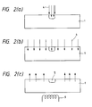
- silicon ion 4 was implanted into a waveguide patterned region on the surface of a quartz glass substrate 1 at an accelerating voltage of 100 keV and in a dose of 1 x 10¹⁷ ions/cm2 [see Fig. 2(a)]. Thereafter, nitrogen ion 4 was implanted into the entire surface of the substrate at an accelerating voltage of 50 keV and in a dose of 1.33 x 10¹⁷ ions/cm2 using an unfocused ion beam implanting apparatus [see Fig. 2(b)]. The substrate was thereafter heated with a heater 6 at 900°C for 1 h as shown in Fig. 2(c) to remove the nitrogen that had been implanted into the non-waveguide area where silicon was not implanted.
- a quartz glass or sapphire substrate 1 was provided and a Cr film 2 which would serve as a mask for ion implantation was formed on the surface of this substrate as shown in Fig. 1(a). Then, openings 3 for an optical waveguide pattern were formed on the Cr film 2 by a well-known photolithographic technique [see Fig. 1(b)]. Subsequently, titanium and oxygen ions 4 were successively implanted into the surface of the masked substrate at respective accelerating voltages of 200 keV and 65 keV [see Fig. 1(c)]. The respective doses of titanium and oxygen ions were 1 x 10¹⁷ ions/cm2 and 2 x 10¹⁷ ions/cm2. Thereafter, the Cr mask 2 was etched away and the substrate was heat-treated at 1,000°C for 1 h. As a result, an optical waveguide 5 composed of a region containing titanium oxide was formed in the substrate 1 [see Fig. 1(d)].
- a focused ion beam implanting apparatus aluminum ion 4 was injected into a waveguide patterned region on the surface of a quartz glass substrate 1 at an accelerating voltage of 150 keV and in a dose of 1 x 10¹⁷ ions/cm2 [see Fig. 2(a)]. Thereafter, nitrogen ion 4 was injected into the entire surface of the substrate at an accelerating voltage of 100 keV and in a dose of 1 x 10¹⁷ ions/cm2 without focusing the ion beam [see Fig. 2(b)]. The substrate was thereafter heat-treated at 1,000°C for 1 h as shown in Fig. 2(c) to remove the nitrogen that had been implanted into the non-waveguide region where aluminum was not implanted. As a result, an optical waveguide 5 composed of a region containing aluminum nitride was formed in the substrate 1.
- a quartz glass substrate 1 was provided and a Cr film 2 which would serve as a mask for ion implantation was formed on the surface of this substrate as shown in Fig. 1(a). Then, openings 3 for an optical waveguide pattern were formed on the Cr film 2 by a well-known photolithographic technique [see Fig. 1(b)]. Subsequently, lithium and chlorine ions 4 were successively implanted into the surface of the masked substrate at respective accelerating voltages of 26 keV and 150 keV [see Fig. 1(c)]. The respective doses of lithium and chlorine ions were 1 x 10¹⁷ ions/cm2. Thereafter, the Cr mask 2 was etched away and the substrate was heat-treated at 1,000°C for 1 h. As a result, an optical waveguide 5 composed of a region containing lithium chloride was formed in the substrate 1 [see Fig. 1(d)].
- a highly heat-stable optical waveguide can be formed on a substrate having high heat resistance, and this enables the fabrication of optoelectronic substrates with an optical waveguide that withstand the manufacturing process of light-emitting and receiving devices.
- a compound that has small absorption of light in the operating wavelength region and that differs greatly from the substrate in terms of refractive index is selected (e.g. silicon nitride has a refractive index of about 2.1 whereas titanium oxide has an index of about 2.5), an optical waveguide can be formed with ions being implanted in smaller amounts to attain the necessary difference in refractive index. This contributes to a lower cost for the formation of waveguides.
- the present invention expands the scope of substrate materials which can be used in the fabrication of optical waveguides.
Landscapes
- Engineering & Computer Science (AREA)
- Physics & Mathematics (AREA)
- Chemical & Material Sciences (AREA)
- General Chemical & Material Sciences (AREA)
- Materials Engineering (AREA)
- Life Sciences & Earth Sciences (AREA)
- Health & Medical Sciences (AREA)
- Chemical Kinetics & Catalysis (AREA)
- Plasma & Fusion (AREA)
- Geochemistry & Mineralogy (AREA)
- Toxicology (AREA)
- Organic Chemistry (AREA)
- Microelectronics & Electronic Packaging (AREA)
- General Physics & Mathematics (AREA)
- Optics & Photonics (AREA)
- Optical Integrated Circuits (AREA)
- Surface Treatment Of Glass (AREA)
Applications Claiming Priority (4)
| Application Number | Priority Date | Filing Date | Title |
|---|---|---|---|
| JP17071/89 | 1989-01-26 | ||
| JP1707189 | 1989-01-26 | ||
| JP1315961A JP2598533B2 (ja) | 1989-01-26 | 1989-12-05 | 光導波路の形成方法 |
| JP315961/89 | 1989-12-05 |
Publications (3)
| Publication Number | Publication Date |
|---|---|
| EP0380138A2 true EP0380138A2 (fr) | 1990-08-01 |
| EP0380138A3 EP0380138A3 (fr) | 1991-10-16 |
| EP0380138B1 EP0380138B1 (fr) | 1994-08-31 |
Family
ID=26353534
Family Applications (1)
| Application Number | Title | Priority Date | Filing Date |
|---|---|---|---|
| EP90101626A Expired - Lifetime EP0380138B1 (fr) | 1989-01-26 | 1990-01-26 | Méthode de fabrication d'un guide d'ondes |
Country Status (4)
| Country | Link |
|---|---|
| US (1) | US5066514A (fr) |
| EP (1) | EP0380138B1 (fr) |
| JP (1) | JP2598533B2 (fr) |
| DE (1) | DE69011882D1 (fr) |
Cited By (4)
| Publication number | Priority date | Publication date | Assignee | Title |
|---|---|---|---|---|
| DE4022090A1 (de) * | 1989-12-18 | 1991-06-20 | Forschungszentrum Juelich Gmbh | Elektro-optisches bauelement und verfahren zu dessen herstellung |
| WO1995013553A1 (fr) * | 1993-11-12 | 1995-05-18 | Schneider Electric S.A. | Fabrication d'un guide d'ondes enterre a plusieurs profondeurs d'enterrement |
| FR2818390A1 (fr) * | 2000-12-15 | 2002-06-21 | Ion Beam Services | Guide d'onde comportant un canal sur un substrat optique |
| WO2018005327A1 (fr) * | 2016-06-28 | 2018-01-04 | Corning Incorporated | Article à base de verre mince ayant une résistance élevée aux dommages par contact |
Families Citing this family (9)
| Publication number | Priority date | Publication date | Assignee | Title |
|---|---|---|---|---|
| US5510154A (en) * | 1992-12-03 | 1996-04-23 | Futaba Denshi Kogyo K.K. | Low-velocity electron excited phosphor and method for producing same |
| US5885665A (en) * | 1997-05-09 | 1999-03-23 | The United States Of America As Represented By The United States Department Of Energy | VO2 precipitates for self-protected optical surfaces |
| JP2000058423A (ja) | 1998-08-12 | 2000-02-25 | Toshiba Corp | 熱処理方法及び熱処理装置 |
| CN100418919C (zh) | 2000-12-20 | 2008-09-17 | 株式会社村田制作所 | 透光性陶瓷及其制造方法和光学元件 |
| US6947651B2 (en) * | 2001-05-10 | 2005-09-20 | Georgia Tech Research Corporation | Optical waveguides formed from nano air-gap inter-layer dielectric materials and methods of fabrication thereof |
| FR2836724B1 (fr) * | 2002-03-01 | 2004-07-23 | Silios Technologies | Adaptateur de mode optique pourvu de deux canaux distincts |
| US7079716B2 (en) * | 2003-06-26 | 2006-07-18 | Bae Systems Information And Electronic Systems Integration Inc. | Integrated photonic circuits with vertical connections |
| SG11201702303WA (en) * | 2014-10-24 | 2017-05-30 | Agc Glass Europe | Ion implantation process and ion implanted glass substrates |
| EP3556911A1 (fr) * | 2018-04-19 | 2019-10-23 | Comadur S.A. | Procédé de structuration d'un motif décoratif ou technique dans un objet réalisé en un matériau amorphe, semi-cristallin ou cristallin au moins partiellement transparent |
Family Cites Families (7)
| Publication number | Priority date | Publication date | Assignee | Title |
|---|---|---|---|---|
| DE2553685C2 (de) * | 1975-11-28 | 1985-05-09 | Siemens AG, 1000 Berlin und 8000 München | Verfahren zur Herstellung eines optischen Richtkopplers |
| US4262056A (en) * | 1978-09-15 | 1981-04-14 | The United States Of America As Represented By The Secretary Of The Navy | Ion-implanted multilayer optical interference filter |
| US4847504A (en) * | 1983-08-15 | 1989-07-11 | Applied Materials, Inc. | Apparatus and methods for ion implantation |
| US4521443A (en) * | 1984-05-07 | 1985-06-04 | Northrop Corporation | Integrated optical waveguide fabrication by ion implantation |
| JPS61209975A (ja) * | 1985-03-14 | 1986-09-18 | 株式会社豊田中央研究所 | 炭化珪素セラミツクス体の強化方法 |
| US4840816A (en) * | 1987-03-24 | 1989-06-20 | The United States Of America As Represented By The United States Department Of Energy | Method of fabricating optical waveguides by ion implantation doping |
| US4789642A (en) * | 1987-03-26 | 1988-12-06 | The United States Of America As Represented By The Secretary Of The Air Force | Method for fabricating low loss crystalline silicon waveguides by dielectric implantation |
-
1989
- 1989-12-05 JP JP1315961A patent/JP2598533B2/ja not_active Expired - Fee Related
-
1990
- 1990-01-18 US US07/466,838 patent/US5066514A/en not_active Expired - Lifetime
- 1990-01-26 DE DE69011882T patent/DE69011882D1/de not_active Expired - Lifetime
- 1990-01-26 EP EP90101626A patent/EP0380138B1/fr not_active Expired - Lifetime
Non-Patent Citations (3)
| Title |
|---|
| APPLIED PHYSICS LETTERS. vol. 22, no. 1, January 1, 1973, NEW YORK US pages 5 - 7; D.T.Y. WEI ET AL.: 'Quartz optical waveguide by ion implantation ' * |
| APPLIED PHYSICS LETTERS. vol. 43, no. 6, September 1983, NEW YORK US pages 519 - 520; I.K. NAIK: 'Low-loss integrated optical waveguides fabricated by nitogen ion implantation ' * |
| PHYSICA. vol. 88, no. 193, 1985, AMSTERDAM NL pages 193 - 205; S. JETSCHKE ET AL.: 'Diffusion and recrystallization processes during annealing of N+- and P+- implanted LiNbO3 ' * |
Cited By (9)
| Publication number | Priority date | Publication date | Assignee | Title |
|---|---|---|---|---|
| DE4022090A1 (de) * | 1989-12-18 | 1991-06-20 | Forschungszentrum Juelich Gmbh | Elektro-optisches bauelement und verfahren zu dessen herstellung |
| US5174876A (en) * | 1989-12-18 | 1992-12-29 | Forschungszentrum Julich Gmbh | Method of making an optical component by ion implantation |
| WO1995013553A1 (fr) * | 1993-11-12 | 1995-05-18 | Schneider Electric S.A. | Fabrication d'un guide d'ondes enterre a plusieurs profondeurs d'enterrement |
| FR2712396A1 (fr) * | 1993-11-12 | 1995-05-19 | Merlin Gerin | Procédé de fabrication d'un dispositif d'optique intégrée et dispositif ainsi fabriqué. |
| US5708750A (en) * | 1993-11-12 | 1998-01-13 | Schneider Electric S.A. | Manufacture of a buried wave guide at several burying depths |
| FR2818390A1 (fr) * | 2000-12-15 | 2002-06-21 | Ion Beam Services | Guide d'onde comportant un canal sur un substrat optique |
| WO2002048747A3 (fr) * | 2000-12-15 | 2002-08-22 | Ion Beam Services | Guide d'onde comportant un canal dans un substrat optique |
| US7756377B2 (en) | 2000-12-15 | 2010-07-13 | Tisserand Stephane | Waveguide comprising a channel on an optical substrate |
| WO2018005327A1 (fr) * | 2016-06-28 | 2018-01-04 | Corning Incorporated | Article à base de verre mince ayant une résistance élevée aux dommages par contact |
Also Published As
| Publication number | Publication date |
|---|---|
| EP0380138B1 (fr) | 1994-08-31 |
| DE69011882D1 (de) | 1994-10-06 |
| JP2598533B2 (ja) | 1997-04-09 |
| US5066514A (en) | 1991-11-19 |
| EP0380138A3 (fr) | 1991-10-16 |
| JPH02275907A (ja) | 1990-11-09 |
Similar Documents
| Publication | Publication Date | Title |
|---|---|---|
| EP0380138B1 (fr) | Méthode de fabrication d'un guide d'ondes | |
| US5979188A (en) | Method of fabricating a planar waveguide structure | |
| EP0812485A1 (fr) | Accord par bande interdite de la structure a puits de semi-conducteur | |
| EP0401971B1 (fr) | Guide d'onde optique et méthode de fabrication | |
| US4521443A (en) | Integrated optical waveguide fabrication by ion implantation | |
| US6544431B2 (en) | Thin film lithium niobate structure and method of making the same | |
| US5193136A (en) | Process for making multifunction integrated optics chips having high electro-optic coefficients | |
| US4145457A (en) | Method for the production of optical directional couplers | |
| US20020048727A1 (en) | Method for forming a refractive-index-patterned film for use in optical device manufacturing | |
| Stein | Thermal Annealing of Si‐N Absorption Bands in Nitrogen‐Implanted Silicon | |
| JPS61204604A (ja) | 光導波路構造の製造法 | |
| JPH0582463A (ja) | P形不純物の拡散方法及び半導体レーザ | |
| US20030091257A1 (en) | Optical waveguide devices and method of fabrication | |
| Naik | Planar And Channel Waveguides Fabricated By Nitrogen Ion Implantation In Fused Silica | |
| US7547608B2 (en) | Polysilicon hard mask for enhanced alignment signal | |
| KR930010830B1 (ko) | 열확산시 산화리튬의 표면 삼출을 방지한 광도파로의 제조방법 | |
| KR0140647B1 (ko) | 위상반전마스크의 제조방법 | |
| EP0425076A2 (fr) | Procédé pour la fabrication des puces à optique intégrée à coefficients électro-optiques élevés | |
| CA2014758A1 (fr) | Methode de preparation d'une couche antidiffusion pour metal alcalin | |
| KR0152212B1 (ko) | 플리머를 다층으로 적층하기 위한 방법 | |
| Chuang et al. | Deep low-loss multimode channel waveguides fabricated on glass substrates using dry silver film electromigration technique | |
| JPH0466099B2 (fr) | ||
| JPS634346B2 (fr) | ||
| Ashley et al. | Low loss ion implanted Ag waveguides in glass | |
| JPH07159638A (ja) | 光導波路デバイスの製造方法 |
Legal Events
| Date | Code | Title | Description |
|---|---|---|---|
| PUAI | Public reference made under article 153(3) epc to a published international application that has entered the european phase |
Free format text: ORIGINAL CODE: 0009012 |
|
| AK | Designated contracting states |
Kind code of ref document: A2 Designated state(s): DE FR GB |
|
| PUAL | Search report despatched |
Free format text: ORIGINAL CODE: 0009013 |
|
| AK | Designated contracting states |
Kind code of ref document: A3 Designated state(s): DE FR GB |
|
| 17P | Request for examination filed |
Effective date: 19920206 |
|
| 17Q | First examination report despatched |
Effective date: 19930809 |
|
| GRAA | (expected) grant |
Free format text: ORIGINAL CODE: 0009210 |
|
| AK | Designated contracting states |
Kind code of ref document: B1 Designated state(s): DE FR GB |
|
| PG25 | Lapsed in a contracting state [announced via postgrant information from national office to epo] |
Ref country code: FR Effective date: 19940831 |
|
| REF | Corresponds to: |
Ref document number: 69011882 Country of ref document: DE Date of ref document: 19941006 |
|
| PG25 | Lapsed in a contracting state [announced via postgrant information from national office to epo] |
Ref country code: DE Effective date: 19941201 |
|
| EN | Fr: translation not filed | ||
| PLBE | No opposition filed within time limit |
Free format text: ORIGINAL CODE: 0009261 |
|
| STAA | Information on the status of an ep patent application or granted ep patent |
Free format text: STATUS: NO OPPOSITION FILED WITHIN TIME LIMIT |
|
| 26N | No opposition filed | ||
| REG | Reference to a national code |
Ref country code: GB Ref legal event code: IF02 |
|
| PGFP | Annual fee paid to national office [announced via postgrant information from national office to epo] |
Ref country code: GB Payment date: 20060125 Year of fee payment: 17 |
|
| GBPC | Gb: european patent ceased through non-payment of renewal fee |
Effective date: 20070126 |
|
| PG25 | Lapsed in a contracting state [announced via postgrant information from national office to epo] |
Ref country code: GB Free format text: LAPSE BECAUSE OF NON-PAYMENT OF DUE FEES Effective date: 20070126 |