EP0380327A2 - Struktur einer Halbleiteranordnung mit einer trichterförmigen Verbindung zwischen den Ebenen - Google Patents
Struktur einer Halbleiteranordnung mit einer trichterförmigen Verbindung zwischen den Ebenen Download PDFInfo
- Publication number
- EP0380327A2 EP0380327A2 EP90300753A EP90300753A EP0380327A2 EP 0380327 A2 EP0380327 A2 EP 0380327A2 EP 90300753 A EP90300753 A EP 90300753A EP 90300753 A EP90300753 A EP 90300753A EP 0380327 A2 EP0380327 A2 EP 0380327A2
- Authority
- EP
- European Patent Office
- Prior art keywords
- contact window
- inter
- film
- insulating film
- level
- Prior art date
- Legal status (The legal status is an assumption and is not a legal conclusion. Google has not performed a legal analysis and makes no representation as to the accuracy of the status listed.)
- Granted
Links
Images



Classifications
-
- H—ELECTRICITY
- H10—SEMICONDUCTOR DEVICES; ELECTRIC SOLID-STATE DEVICES NOT OTHERWISE PROVIDED FOR
- H10W—GENERIC PACKAGES, INTERCONNECTIONS, CONNECTORS OR OTHER CONSTRUCTIONAL DETAILS OF DEVICES COVERED BY CLASS H10
- H10W20/00—Interconnections in chips, wafers or substrates
- H10W20/40—Interconnections external to wafers or substrates, e.g. back-end-of-line [BEOL] metallisations or vias connecting to gate electrodes
- H10W20/41—Interconnections external to wafers or substrates, e.g. back-end-of-line [BEOL] metallisations or vias connecting to gate electrodes characterised by their conductive parts
- H10W20/42—Vias, e.g. via plugs
Definitions
- This invention relates to a semiconductor device and, more particularly, to the structure of an interconnection between a lower conductive layer and an upper conductive layer.
- a semiconductor device is fabricated into a multiple level structure, and inter-level connections provide the electrical paths between the different levels.
- an upper level wiring strip per se provides the inter-level connection, and such an inter-level connection is produced through the following steps. Namely, when a lower level conductive film is formed, an inter-level insulating film is deposited over the entire surface, and a contact window is, then, formed in the inter-level conductive layer for partially exposing the lower level conductive layer. An conductive metal such as aluminum is deposited over the entire surface, so that the aluminum film penetrates into the contact window, then being patterned so as to form the upper level wiring strip. In this example, a smooth topography hardly takes place, and, accordingly, a poor coverage is causative of undesirable disconnection.
- an n-type impurity region 1 is formed in a p-type silicon substrate 2, and phosphosilicate glass is deposited to a thickness of about 5000 angstroms over the entire surface of the structure by using a chemical vapor deposition technique.
- the phosphosilicate glass film 3 is anisotropically etched away by using a reactive etching technique to from a contact window 4, and a polysilicon is deposited to a thickness of about 1 micron by using an usual chemical vapor deposition technique.
- the contact window 4 is formed in the phosphosilicate glass film 3, the polysilicon fills the contact window and further spreads over the phosphosilicate glass film 3, thereby providing a generally flat top surface.
- the polysilicon thus deposited is uniformly removed through an etch-back technique until the to p surface of the phosphosilicate glass film 3 is exposed, so that a piece of polysilicon 5 is left in the contact window 4.
- an aluminum is deposited over the entire surface by using a sputtering technique, and the aluminum film is patterned to form an upper wiring strip 6.
- the present invention proposes to form a funnel shaped inter-level connection.
- a semiconductor device having at least one transistor, comprising a) a lower conductive layer; b) an inter-level insulating film structure provided on the lower conductive layer, a contact window being formed in the inter-level insulating film structure; c) an inter-level connection provided in the contact window and contacting at the bottom surface thereof with the lower conductive layer; and d) an upper conductive layer formed on the inter-level insulating film structure and electrically connected to the inter-level connection, in which the inter-level insulating film structure comprises a lower insulating film having a lower part of the contact window and an upper insulating film having an upper part of the contact window, and in which the lower part of the contact window is smaller in cross sectional area than the upper part of the contact window.
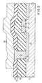
- a semiconductor device is fabricated on a p-type single crystal silicon substrate 21.
- n-type source and drain regions 22 and 23 which are spaced apart from each other by a channel forming area 24.
- a thin gate oxide film 25 is grown over the channel forming area 24, and a gate electrode 26 is provided on the gate oxide film 25.
- the source and drain regions 22 and 23, the gate oxide film 25 and the gate electrode 26 as a whole constitute a field effect transistor.
- a large number of field effect transistors are formed on the silicon substrate 21, however, only one the field effect transistor is shown in Fig. 2 for the sake of simple illustration.
- the silicon substrate 21 as well as the gate electrode 26 are covered with an inter-level insulating film structure 27 consisting of a lower insulating film 28 of a phosphosilicate glass film 28 and an upper insulating film 29 of a silicon oxide, and a contact window 30 is formed in the inter-level insulating film structure 27.
- the contact window has lower and upper portions passing through the lower insulating film 28 and the upper insulating film 29, respectively, and the lower portion is smaller in the cross sectional area than the upper portion.
- the contact window thus shaped is of the generally funnel configuration.
- the funnel shaped contact window 30 is partially filled with a piece of an n-type impurity doped polysilicon 31 the top surface of which is slightly lower than the top surface of the upper insulating film 29.
- On the inter-level insulating film structure 27 extends an upper wiring strip 32 of an aluminum which is in contact with the piece of the polysilicon 31.
- the upper wiring strip 32 serves as, for example, a power supply line, and the electric power is supplied through the upper wiring strip 32 and the piece of polysilicon 31 to the source region 22 of the field effect transistor.
- the single crystal silicon substrate 21 is prepared, and the thin gate oxide film 25 is thermally grown on the silicon substrate 21. Subsequently, n-type impurity atoms are doped into the silicon substrate 21 so as to form the source and drain regions 22 and 23 in a self-align fashion with respect to the gate electrode 26. An essential part of the resultant structure is shown in Fig. 3A.
- the phosphosilicate glass is firstly deposited to a thickness of about 5000 angstroms on the entire surface of the structure by using a chemical vapor deposition technique, and silicon dioxide is, then, deposited to a thickness of about 1000 angstroms on the phosphosilicate glass film 28 by using a usual chemical vapor deposition technique.
- the phosphosilicate glass is smaller in etching rate than the silicon dioxide. In fact, the phosphosilicate glass is of the order of 450 angstroms per minute, but the silicon dioxide is as large as 800 angstroms per minute. The resultant structure of this stage is shown in Fig. 3B.
- a photoresist solution is spun onto the silicon dioxide film 29, and is, then, patterned through usual lithographic techniques so that a mask layer 33 is provided on the silicon dioxide film 29.
- the mask layer 33 exposes a part of the silicon dioxide film 29 where the upper portion of the funnel shaped contact window 30 will be shaped in the later stage.
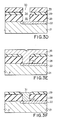
- the exposed area of the silicon dioxide film 29 is isotropically etched by using a wet etching technique as shown in Fig. 3C, and the recess 34 formed in the silicon dioxide film 29 is about 2 micron in diameter. Since the recess 34 is formed in an isotropical manner, the upper periphery of the recess 34 extends beneath the bottom surface of the mask layer 33.
- the phosphosilicate glass film 28 is anisotropically etched by using the mask layer 33, and a hollow space 35 is formed in the phosphosilicate glass film 28.
- the hollow space 35 is square in cross section, and the square is measured as 1 micron x 1 micron.
- the recess 34 and the hollow space 35 form in combination the funnel shaped contact window 30 as shown in Fig. 3D.
- a polysilicon 36 is then deposited to a thickness of about 1 micron over the entire surface of the structure, and the polysilicon 36 penetrates into the funnel shaped contact window 30.
- the resultant structure of this stage is shown in Fig. 3E.
- etch-back technique is, then, applied to the polysilicon film 36.
- the polysilicon film 36 is isotropically etched away by using a dry etching technique until the top surface of the silicon dioxide film 29 is exposed.
- the top surface of the piece of the polysilicon 31 may be slightly lowered with respect to the top surface of the silicon dioxide film 29 because of the unequal top surface of the doped polysilicon 36.
- the top surface of the piece of the polysilicon 31 is much closer to the top surface of the silicon dioxide film 29 by virtue of the funnel shaped contact window 30.
- N-type impurity atoms are ion implanted into the piece of the polysilicon 31 for providing an ohmic contact. The resultant structure of this stage is shown in Fig. 3F.
- FIG. 4 of the drawings another semiconductor device is fabricated on a p-type single crystal silicon substrate 41, and the semiconductor device has a field effect transistor which is formed with n-type source and drain regions 42 and 43, a gate oxide film 44 and a gate electrode 45.
- An insulating film 46 covers the semiconductor substrate 41 and the field effect transistor, and a lower conductive film 47 of a polysilicon is brought into contact with the source region 42 through a contact window formed in the insulating film 46.
- an inter-level insulating film structure 48 which consists of a lower insulating film 49 of a phosphosilicate glass and an upper insulating film 50 of silicon dioxide.
- a funnel shaped contact window 51 is formed in the inter-level insulating film structure 48, and is filled with an n-type impurity doped polysilicon 52.
- On the inter-level insulating film structure 48 is patterned an upper wiring strip 53 of an aluminum which is in contact with the piece of the doped polysilicon 52 for electrical conduction.
- a passivation film 54 is deposited over the entire surface of the structure for providing protection.
- the funnel shaped contact window 51 is also effective for preventing the upper wiring strip 53 from undesirable cracks.
- the process sequence is similar to that illustrated in Figs. 3A to 3F, and, for this reason no description is incorporated.
- the funnel shaped contact window according to the present invention is advantageous over the prior art column shaped contact window in the improved coverage and in the smooth topography.
Landscapes
- Internal Circuitry In Semiconductor Integrated Circuit Devices (AREA)
- Electrodes Of Semiconductors (AREA)
Applications Claiming Priority (2)
| Application Number | Priority Date | Filing Date | Title |
|---|---|---|---|
| JP16723/89 | 1989-01-25 | ||
| JP1016723A JP2623812B2 (ja) | 1989-01-25 | 1989-01-25 | 半導体装置の製造方法 |
Publications (3)
| Publication Number | Publication Date |
|---|---|
| EP0380327A2 true EP0380327A2 (de) | 1990-08-01 |
| EP0380327A3 EP0380327A3 (de) | 1990-12-12 |
| EP0380327B1 EP0380327B1 (de) | 1997-10-15 |
Family
ID=11924185
Family Applications (1)
| Application Number | Title | Priority Date | Filing Date |
|---|---|---|---|
| EP90300753A Expired - Lifetime EP0380327B1 (de) | 1989-01-25 | 1990-01-24 | Halbleiteranordnung mit einer trichterförmigen Verbindung zwischen Leiter-Ebenen und Verfahren zu ihrer Herstellung |
Country Status (4)
| Country | Link |
|---|---|
| US (1) | US5091768A (de) |
| EP (1) | EP0380327B1 (de) |
| JP (1) | JP2623812B2 (de) |
| DE (1) | DE69031575T2 (de) |
Cited By (11)
| Publication number | Priority date | Publication date | Assignee | Title |
|---|---|---|---|---|
| EP0503904A3 (en) * | 1991-03-15 | 1992-11-19 | Mitsubishi Denki Kabushiki Kaisha | Contact structure of an interconnection layer placed on a surface having steps and sram having a multilayer interconnection and manufacturing method thereof |
| GB2265254A (en) * | 1992-03-17 | 1993-09-22 | Mitsubishi Electric Corp | A semiconductor device with planarized insulating layers |
| EP0738005A3 (de) * | 1995-04-11 | 1996-12-04 | Sgs Thomson Microelectronics | Verfahren zur Herstellung einer Kontaktfläche in einer integrierten Schaltung |
| US5585307A (en) * | 1995-02-27 | 1996-12-17 | Taiwan Semiconductor Manufacturing Company Ltd. | Forming a semi-recessed metal for better EM and Planarization using a silo mask |
| EP0524818B1 (de) * | 1991-07-23 | 1997-10-08 | Nec Corporation | Mehrlagige Verbindungsstruktur für eine Halbleiter- vorrichtung und Verfahren zu ihrer Herstellung |
| FR2754391A1 (fr) * | 1996-10-08 | 1998-04-10 | Sgs Thomson Microelectronics | Structure de contact a facteur de forme eleve pour circuits integres |
| US5894160A (en) * | 1994-05-31 | 1999-04-13 | Stmicroelectronics, Inc. | Method of forming a landing pad structure in an integrated circuit |
| US5909636A (en) * | 1994-12-22 | 1999-06-01 | Stmicroelectronics, Inc. | Method of forming a landing pad structure in an integrated circuit |
| US5914518A (en) * | 1994-05-31 | 1999-06-22 | Stmicroelectronics, Inc. | Method of forming a metal contact to landing pad structure in an integrated circuit |
| US5945738A (en) * | 1994-05-31 | 1999-08-31 | Stmicroelectronics, Inc. | Dual landing pad structure in an integrated circuit |
| DE102004044686A1 (de) * | 2004-09-15 | 2006-03-16 | Infineon Technologies Ag | Integrierte Schaltungsanordnung mit Vias, die zwei Abschnitte haben, und Herstellungsverfahren |
Families Citing this family (17)
| Publication number | Priority date | Publication date | Assignee | Title |
|---|---|---|---|---|
| JPH073835B2 (ja) * | 1990-03-19 | 1995-01-18 | 日本プレシジョン・サーキッツ株式会社 | 半導体装置 |
| JPH06125013A (ja) * | 1992-03-14 | 1994-05-06 | Toshiba Corp | 半導体装置及びその製造方法 |
| US5365082A (en) * | 1992-09-30 | 1994-11-15 | Texas Instruments Incorporated | MOSFET cell array |
| US5783471A (en) * | 1992-10-30 | 1998-07-21 | Catalyst Semiconductor, Inc. | Structure and method for improved memory arrays and improved electrical contacts in semiconductor devices |
| JP2684978B2 (ja) * | 1993-11-25 | 1997-12-03 | 日本電気株式会社 | 半導体装置 |
| US5777486A (en) * | 1994-10-03 | 1998-07-07 | United Microelectronics Corporation | Electromigration test pattern simulating semiconductor components |
| JPH09102541A (ja) * | 1995-10-05 | 1997-04-15 | Mitsubishi Electric Corp | 半導体装置及びその製造方法 |
| WO1997019469A1 (en) * | 1995-11-22 | 1997-05-29 | Olin Corporation | Semiconductor package with ground or power ring |
| US5994220A (en) | 1996-02-02 | 1999-11-30 | Micron Technology, Inc. | Method for forming a semiconductor connection with a top surface having an enlarged recess |
| KR0176199B1 (ko) * | 1996-03-19 | 1999-04-15 | 김광호 | 반도체 소자의 접촉창 형성방법 |
| US5950104A (en) * | 1997-04-09 | 1999-09-07 | Vanguard International Semiconductor Corporation | Contact process using Y-contact etching |
| WO1999004427A1 (de) | 1997-07-15 | 1999-01-28 | Infineon Technologies Ag | Kontaktierung einer halbleiterzone |
| JP3445495B2 (ja) * | 1997-07-23 | 2003-09-08 | 株式会社東芝 | 半導体装置 |
| US6777738B2 (en) * | 1999-06-09 | 2004-08-17 | Renesas Technology Corp. | Semiconductor integrated circuit |
| JP5835696B2 (ja) * | 2012-09-05 | 2015-12-24 | 株式会社東芝 | 半導体装置およびその製造方法 |
| KR20140104778A (ko) * | 2013-02-21 | 2014-08-29 | 삼성전자주식회사 | 관통전극을 갖는 반도체 소자의 제조방법 |
| CN119866044B (zh) * | 2025-03-19 | 2025-08-22 | 赛晶亚太半导体科技(浙江)有限公司 | 一种具有终接区和钝化层的半导体器件及制备方法 |
Family Cites Families (15)
| Publication number | Priority date | Publication date | Assignee | Title |
|---|---|---|---|---|
| JPS592352A (ja) * | 1982-06-28 | 1984-01-07 | Toshiba Corp | 半導体装置の製造方法 |
| GB8312850D0 (en) * | 1983-05-10 | 1983-06-15 | British Telecomm | Semiconductor wafer fabrication |
| JPS601846A (ja) * | 1983-06-18 | 1985-01-08 | Toshiba Corp | 多層配線構造の半導体装置とその製造方法 |
| JPS6030153A (ja) * | 1983-07-28 | 1985-02-15 | Toshiba Corp | 半導体装置 |
| JPS6068613A (ja) * | 1983-09-26 | 1985-04-19 | Oki Electric Ind Co Ltd | 半導体装置の製造方法 |
| GB8401250D0 (en) * | 1984-01-18 | 1984-02-22 | British Telecomm | Semiconductor fabrication |
| JPS60163455A (ja) * | 1984-02-03 | 1985-08-26 | Toshiba Corp | 読み出し専用記憶装置及びその製造方法 |
| JPS61166071A (ja) * | 1985-01-17 | 1986-07-26 | Toshiba Corp | 半導体装置及びその製造方法 |
| US4692786A (en) * | 1985-02-07 | 1987-09-08 | Lindenfelser Timothy M | Semi-conductor device with sandwich passivation coating |
| FR2588417B1 (fr) * | 1985-10-03 | 1988-07-29 | Bull Sa | Procede de formation d'un reseau metallique multicouche d'interconnexion des composants d'un circuit integre de haute densite et circuit integre en resultant |
| JPS62139322A (ja) * | 1985-12-12 | 1987-06-23 | Fujitsu Ltd | 電子ビ−ム露光方法 |
| JPS62198135A (ja) * | 1986-02-26 | 1987-09-01 | Nec Corp | 半導体装置およびその製造方法 |
| JPS633437A (ja) * | 1986-06-23 | 1988-01-08 | Sony Corp | 半導体装置の製造方法 |
| JPS63244862A (ja) * | 1987-03-31 | 1988-10-12 | Nec Corp | 半導体装置 |
| JPH0748517B2 (ja) * | 1987-06-25 | 1995-05-24 | 日本電気株式会社 | 半導体集積回路装置 |
-
1989
- 1989-01-25 JP JP1016723A patent/JP2623812B2/ja not_active Expired - Fee Related
-
1990
- 1990-01-18 US US07/467,122 patent/US5091768A/en not_active Expired - Lifetime
- 1990-01-24 EP EP90300753A patent/EP0380327B1/de not_active Expired - Lifetime
- 1990-01-24 DE DE69031575T patent/DE69031575T2/de not_active Expired - Fee Related
Cited By (23)
| Publication number | Priority date | Publication date | Assignee | Title |
|---|---|---|---|---|
| US5581093A (en) * | 1991-03-15 | 1996-12-03 | Mitsubishi Denki Kabushiki Kaisha | Contact structure of an interconnection layer for a semiconductor device and a multilayer interconnection SRAM |
| EP0503904A3 (en) * | 1991-03-15 | 1992-11-19 | Mitsubishi Denki Kabushiki Kaisha | Contact structure of an interconnection layer placed on a surface having steps and sram having a multilayer interconnection and manufacturing method thereof |
| US5475240A (en) * | 1991-03-15 | 1995-12-12 | Mitsubishi Denki Kabushiki Kaisha | Contact structure of an interconnection layer for a semiconductor device and a multilayer interconnection SRAM |
| US5654239A (en) * | 1991-03-15 | 1997-08-05 | Mitsubishi Denki Kabushiki Kaisha | Method of manufacturing a contact structure of an interconnection layer for a semiconductor device and a multilayer interconnection SRAM |
| EP0524818B1 (de) * | 1991-07-23 | 1997-10-08 | Nec Corporation | Mehrlagige Verbindungsstruktur für eine Halbleiter- vorrichtung und Verfahren zu ihrer Herstellung |
| US5930674A (en) * | 1992-03-17 | 1999-07-27 | Mitsubishi Denki Kabushiki Kaisha | Semiconductor device with improved planarization properties |
| GB2265254B (en) * | 1992-03-17 | 1996-03-13 | Mitsubishi Electric Corp | A semiconductor chip and a method of manufacture thereof |
| US5479054A (en) * | 1992-03-17 | 1995-12-26 | Mitsubishi Denki Kabushiki Kaisha | Semiconductor device with improved planarization properties |
| GB2265254A (en) * | 1992-03-17 | 1993-09-22 | Mitsubishi Electric Corp | A semiconductor device with planarized insulating layers |
| US5914518A (en) * | 1994-05-31 | 1999-06-22 | Stmicroelectronics, Inc. | Method of forming a metal contact to landing pad structure in an integrated circuit |
| US5956615A (en) * | 1994-05-31 | 1999-09-21 | Stmicroelectronics, Inc. | Method of forming a metal contact to landing pad structure in an integrated circuit |
| US5945738A (en) * | 1994-05-31 | 1999-08-31 | Stmicroelectronics, Inc. | Dual landing pad structure in an integrated circuit |
| US5894160A (en) * | 1994-05-31 | 1999-04-13 | Stmicroelectronics, Inc. | Method of forming a landing pad structure in an integrated circuit |
| US5705427A (en) * | 1994-12-22 | 1998-01-06 | Sgs-Thomson Microelectronics, Inc. | Method of forming a landing pad structure in an integrated circuit |
| US5909636A (en) * | 1994-12-22 | 1999-06-01 | Stmicroelectronics, Inc. | Method of forming a landing pad structure in an integrated circuit |
| US6093963A (en) * | 1994-12-22 | 2000-07-25 | Stmicroelectronics, Inc. | Dual landing pad structure including dielectric pocket |
| USRE36938E (en) * | 1994-12-22 | 2000-10-31 | Stmicroelectronics, Inc. | Method of forming a landing pad structure in an integrated circuit |
| US5585307A (en) * | 1995-02-27 | 1996-12-17 | Taiwan Semiconductor Manufacturing Company Ltd. | Forming a semi-recessed metal for better EM and Planarization using a silo mask |
| EP0738005A3 (de) * | 1995-04-11 | 1996-12-04 | Sgs Thomson Microelectronics | Verfahren zur Herstellung einer Kontaktfläche in einer integrierten Schaltung |
| FR2754391A1 (fr) * | 1996-10-08 | 1998-04-10 | Sgs Thomson Microelectronics | Structure de contact a facteur de forme eleve pour circuits integres |
| DE102004044686A1 (de) * | 2004-09-15 | 2006-03-16 | Infineon Technologies Ag | Integrierte Schaltungsanordnung mit Vias, die zwei Abschnitte haben, und Herstellungsverfahren |
| DE102004044686B4 (de) * | 2004-09-15 | 2006-08-31 | Infineon Technologies Ag | Integrierte Schaltungsanordnung mit Vias, die zwei Abschnitte haben, und Herstellungsverfahren |
| US8273658B2 (en) | 2004-09-15 | 2012-09-25 | Infineon Technologies Ag | Integrated circuit arrangement including vias having two sections, and method for producing the same |
Also Published As
| Publication number | Publication date |
|---|---|
| EP0380327A3 (de) | 1990-12-12 |
| US5091768A (en) | 1992-02-25 |
| DE69031575T2 (de) | 1998-02-12 |
| JPH02196420A (ja) | 1990-08-03 |
| DE69031575D1 (de) | 1997-11-20 |
| JP2623812B2 (ja) | 1997-06-25 |
| EP0380327B1 (de) | 1997-10-15 |
Similar Documents
| Publication | Publication Date | Title |
|---|---|---|
| US5091768A (en) | Semiconductor device having a funnel shaped inter-level connection | |
| US5330934A (en) | Method of fabricating a semiconductor device having miniaturized contact electrode and wiring structure | |
| US4102733A (en) | Two and three mask process for IGFET fabrication | |
| US4833519A (en) | Semiconductor device with a wiring layer having good step coverage for contact holes | |
| US4329706A (en) | Doped polysilicon silicide semiconductor integrated circuit interconnections | |
| US5366914A (en) | Vertical power MOSFET structure having reduced cell area | |
| EP0435388B1 (de) | Verfahren zum teilweisen Anfüllen von Kontakten oder Durchführungen verschiedener Tiefe | |
| JP3413876B2 (ja) | 半導体装置 | |
| US5541434A (en) | Semiconductor device incorporating a contact for electrically connecting adjacent portions within the semiconductor device | |
| JPH0391930A (ja) | 半導体装置の製造方法 | |
| US4364166A (en) | Semiconductor integrated circuit interconnections | |
| US4348802A (en) | Process for producing a semiconductor device | |
| JP3123092B2 (ja) | 半導体装置の製造方法 | |
| US4737831A (en) | Semiconductor device with self-aligned gate structure and manufacturing process thereof | |
| JPS6144470A (ja) | 集積回路チップにおける金属充填方法 | |
| KR0173458B1 (ko) | 반도체집적회로 및 그 제조방법 | |
| US4908679A (en) | Low resistance Schottky diode on polysilicon/metal-silicide | |
| JP3108447B2 (ja) | 半導体装置及びその製造方法 | |
| EP0239746A2 (de) | Verfahren zur Herstellung von Halbleiterbauelementen | |
| KR950009818B1 (ko) | 쇼트키 장벽 다이오드를 포함하는 반도체 장치 및 그 제조방법 | |
| US5439832A (en) | Method for fabricating semiconductor device | |
| JP2000349289A (ja) | 半導体装置およびその製造方法 | |
| US6351038B1 (en) | Integrated circuitry | |
| JPH0415619B2 (de) | ||
| US4876581A (en) | Field effect transistor with short channel length and process of fabrication thereof |
Legal Events
| Date | Code | Title | Description |
|---|---|---|---|
| PUAI | Public reference made under article 153(3) epc to a published international application that has entered the european phase |
Free format text: ORIGINAL CODE: 0009012 |
|
| 17P | Request for examination filed |
Effective date: 19900208 |
|
| AK | Designated contracting states |
Kind code of ref document: A2 Designated state(s): DE FR GB |
|
| PUAL | Search report despatched |
Free format text: ORIGINAL CODE: 0009013 |
|
| AK | Designated contracting states |
Kind code of ref document: A3 Designated state(s): DE FR GB |
|
| 17Q | First examination report despatched |
Effective date: 19931116 |
|
| GRAG | Despatch of communication of intention to grant |
Free format text: ORIGINAL CODE: EPIDOS AGRA |
|
| GRAH | Despatch of communication of intention to grant a patent |
Free format text: ORIGINAL CODE: EPIDOS IGRA |
|
| GRAH | Despatch of communication of intention to grant a patent |
Free format text: ORIGINAL CODE: EPIDOS IGRA |
|
| GRAA | (expected) grant |
Free format text: ORIGINAL CODE: 0009210 |
|
| AK | Designated contracting states |
Kind code of ref document: B1 Designated state(s): DE FR GB |
|
| REF | Corresponds to: |
Ref document number: 69031575 Country of ref document: DE Date of ref document: 19971120 |
|
| ET | Fr: translation filed | ||
| PLBE | No opposition filed within time limit |
Free format text: ORIGINAL CODE: 0009261 |
|
| STAA | Information on the status of an ep patent application or granted ep patent |
Free format text: STATUS: NO OPPOSITION FILED WITHIN TIME LIMIT |
|
| 26N | No opposition filed | ||
| REG | Reference to a national code |
Ref country code: GB Ref legal event code: IF02 |
|
| REG | Reference to a national code |
Ref country code: GB Ref legal event code: 732E |
|
| REG | Reference to a national code |
Ref country code: FR Ref legal event code: TQ |
|
| REG | Reference to a national code |
Ref country code: GB Ref legal event code: 732E |
|
| REG | Reference to a national code |
Ref country code: FR Ref legal event code: TQ Ref country code: FR Ref legal event code: TP |
|
| PGFP | Annual fee paid to national office [announced via postgrant information from national office to epo] |
Ref country code: DE Payment date: 20070118 Year of fee payment: 18 |
|
| PGFP | Annual fee paid to national office [announced via postgrant information from national office to epo] |
Ref country code: GB Payment date: 20070124 Year of fee payment: 18 |
|
| PGFP | Annual fee paid to national office [announced via postgrant information from national office to epo] |
Ref country code: FR Payment date: 20070109 Year of fee payment: 18 |
|
| GBPC | Gb: european patent ceased through non-payment of renewal fee |
Effective date: 20080124 |
|
| PG25 | Lapsed in a contracting state [announced via postgrant information from national office to epo] |
Ref country code: DE Free format text: LAPSE BECAUSE OF NON-PAYMENT OF DUE FEES Effective date: 20080801 |
|
| REG | Reference to a national code |
Ref country code: FR Ref legal event code: ST Effective date: 20081029 |
|
| PG25 | Lapsed in a contracting state [announced via postgrant information from national office to epo] |
Ref country code: GB Free format text: LAPSE BECAUSE OF NON-PAYMENT OF DUE FEES Effective date: 20080124 |
|
| PG25 | Lapsed in a contracting state [announced via postgrant information from national office to epo] |
Ref country code: FR Free format text: LAPSE BECAUSE OF NON-PAYMENT OF DUE FEES Effective date: 20080131 |