EP0381464A2 - Übertragung von Signalen mit hoher Bandbreite über ein Koaxialkabel - Google Patents
Übertragung von Signalen mit hoher Bandbreite über ein Koaxialkabel Download PDFInfo
- Publication number
- EP0381464A2 EP0381464A2 EP90300978A EP90300978A EP0381464A2 EP 0381464 A2 EP0381464 A2 EP 0381464A2 EP 90300978 A EP90300978 A EP 90300978A EP 90300978 A EP90300978 A EP 90300978A EP 0381464 A2 EP0381464 A2 EP 0381464A2
- Authority
- EP
- European Patent Office
- Prior art keywords
- signal
- time delayed
- cable
- serial
- input
- Prior art date
- Legal status (The legal status is an assumption and is not a legal conclusion. Google has not performed a legal analysis and makes no representation as to the accuracy of the status listed.)
- Granted
Links
- 230000007704 transition Effects 0.000 claims abstract description 34
- 238000000034 method Methods 0.000 claims abstract description 17
- 230000003111 delayed effect Effects 0.000 claims description 23
- 230000008878 coupling Effects 0.000 claims description 5
- 238000010168 coupling process Methods 0.000 claims description 5
- 238000005859 coupling reaction Methods 0.000 claims description 5
- 230000002238 attenuated effect Effects 0.000 claims description 4
- 230000004069 differentiation Effects 0.000 abstract description 4
- 230000005540 biological transmission Effects 0.000 description 12
- 238000004891 communication Methods 0.000 description 5
- 238000013459 approach Methods 0.000 description 3
- 239000003990 capacitor Substances 0.000 description 3
- 238000013461 design Methods 0.000 description 3
- 239000000835 fiber Substances 0.000 description 3
- 230000000903 blocking effect Effects 0.000 description 2
- 238000001514 detection method Methods 0.000 description 2
- 238000010586 diagram Methods 0.000 description 2
- 230000005291 magnetic effect Effects 0.000 description 2
- 230000001702 transmitter Effects 0.000 description 2
- 230000003321 amplification Effects 0.000 description 1
- 230000008859 change Effects 0.000 description 1
- 230000000694 effects Effects 0.000 description 1
- 230000036039 immunity Effects 0.000 description 1
- 238000003199 nucleic acid amplification method Methods 0.000 description 1
- 238000011084 recovery Methods 0.000 description 1
- 230000008054 signal transmission Effects 0.000 description 1
- 238000012546 transfer Methods 0.000 description 1
Images

Classifications
-
- H—ELECTRICITY
- H04—ELECTRIC COMMUNICATION TECHNIQUE
- H04L—TRANSMISSION OF DIGITAL INFORMATION, e.g. TELEGRAPHIC COMMUNICATION
- H04L25/00—Baseband systems
- H04L25/38—Synchronous or start-stop systems, e.g. for Baudot code
- H04L25/40—Transmitting circuits; Receiving circuits
- H04L25/49—Transmitting circuits; Receiving circuits using code conversion at the transmitter; using predistortion; using insertion of idle bits for obtaining a desired frequency spectrum; using three or more amplitude levels ; Baseband coding techniques specific to data transmission systems
- H04L25/4904—Transmitting circuits; Receiving circuits using code conversion at the transmitter; using predistortion; using insertion of idle bits for obtaining a desired frequency spectrum; using three or more amplitude levels ; Baseband coding techniques specific to data transmission systems using self-synchronising codes, e.g. split-phase codes
Definitions
- the present invention is directed to method and apparatus for transmitting high-bandwidth signals on coaxial cable, and more particularly to method and apparatus for decoding such signals utilizing a novel differential comparator technique.
- Point-to-point data communication over coaxial or fiber optic media can be implemented using a general purpose interface such as the AMD AM7968 taxi chip transmitter and AM7969 taxi chip receiver.
- a general purpose interface such as the AMD AM7968 taxi chip transmitter and AM7969 taxi chip receiver.
- These devices whose characteristics are described in AMD Publication No. 07370, issued May 1987 and incorporated herein by reference, provide for very high speed point-to-point communications by loading data into the input side of the transmitter chip, and outputting it on the output side of the receiver chip, the chips being separated by a serial cable of indeterminate length.
- a complete link suitable for full-duplex communication would consist of two such serial data links, one for each direction.
- each transition of the transmitted chips output signal corresponding to a one, and the lack of a transition corresponding to a zero.
- each 1 is represented as a transition. The direction of the transition in this scheme is not relevant.
- the transmitting chip incorporates means for implementing a run length limited (RLL) coding technique that allows transmission of 100 megabit per second data on a 125 megabit per second channel.
- RLL run length limited
- the output codes While there are 16 combinations of each 4-bit nibble that is to be encoded, there are 32 possible combinations of resultant 5-bit code. Therefore, in addition to minimizing the number of consecutive zeros in the output code, the output codes also have the characteristic that a minimum number of zeros appear at either end of the 5-bit output.
- the maximum time between transitions is 3-bit times, and the minimum time between transitions being 1-bit time (a bit time being defined as 8 nanoseconds).
- the frequency is half of that or 62.5 megahertz at its maximum rate, the minimum rate being one fourth of that or about 13.1 megahertz.
- a second type of links may be constructed.
- One uses fiber optics which allows signal transmission over long distance with minimal attenuation, but at high cost.
- a second type also uses the above-described data transmission protocol, but using inexpensive coaxial cable as the transmission medium.
- the problem to be addressed by the present invention is the potential loss of accuracy when a signal encoded according to the method described above is transmitted on coaxial cable.
- the result of such transition is attenuation of the transmitted signal. It is known that the signal will be distorted since the cable behaves as a low pass filter. Low frequency components (strings of zeros, without transitions) reach higher amplitudes than high frequency components (strings of ones, having transitions at an 8 nanosecond rate).
- a pattern consisting of ...00011000... cannot be reliably detected by simply comparing the voltage on the cable with a fixed slicing level (typically zero).
- An alternative approach would be to use a technique wherein instead of looking at the magnitudes of the signals, the detection system looks at the transitions of the signals as is done in magnetic disc recording.
- the difficulty with implementing this approach in a coaxial cable data transmission scheme is that the frequency of transmission under consideration here is orders of magnitude faster than the rate at which data is being read in a magnetic recording scheme.
- a high bandwidth signal may be transmitted on a coaxial cable and accurately decoded by providing at the receiving end a receiving circuit which is not sensitive to the amplitude of the received signal, but is responsive only to the time at which transition of the signal occurs.
- signals meeting the requirement are provided by differentiating the received signal which is transmitted in a code wherein zeros are indicated by a lack of transition, and ones are indicated by a transition, the differentiation providing an indication of the time at which the transition occurs.
- the signal which was originally transmitted is reconstructed by comparing the signal which is received at the end of the coaxial cable, with a signal received at a time T+ ⁇ T, in a standard differential comparator.
- V OUT (T) K1*(V IN (T) - K2*V IN (T) - ⁇ T).
- V IN is the received signal at the end of the serial cable
- V OUT is the signal provided to the receiver chip for decoding.
- K1 is the gain of the differential comparator, which is a standard chip.
- K2 is defined by the ratio of a pair of series connected resistors connected between one end of a delay line having a characteristic delay ⁇ T and ground. The connecting point between the two resistors is connected to one input of the comparator, the other input of the comparator being connected directly to the serial cable output. By choosing the sum of the two resistors to be equal to the characteristic line impedance of the coaxial cable, these resistors also provide the desired termination impedance for the cable. The output of the comparator is connected directly to the receiver chip.
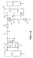
- the implementation of the coaxial transmitting and receiving system of the present invention is shown, for example, in FIG. 2.
- the method implemented using this configuration will allow error-free recovery of RLL encoded data transmitted over long distances (several hundred feet) at high speeds (100 to 125 megabits per second) on inexpensive coaxial cable.
- the transmitter and receiver circuits 2, 4 are standard integrated circuit chips of which typical examples are the AM7968 and AM7969 integrated circuit chips made by Advanced Micro Devices. These transmitter and receiver chips are general purpose interfaces for very high speed (4 to 12.5 megabyte per second, 40-125 megabaud serially) point-to-point communication over coaxial or fiber optic media.
- Each chip 2, 4 emulates a pseudo parallel register.
- the chip loads data into one side and outputs it on the other, in this case the output side 8 of transmitter 2 is separated from input side 9 of receiver 4 by a long serial link which in the present embodiment comprises a coaxial cable 6.
- the speed of a system is adjustable over a range of frequencies with parallel bus transfer rates from 4 megabytes per second to 12.5 megabytes per second.
- the differential ECL signal produced at the output 8 of the transmitter chip 2 is transformer-coupled across transformer 10 to the coaxial cable 6.
- Capacitors 12 and 14 are provided for DC blocking at the output of the transmitter 2, and do not have a critical value.
- Resistors 16, 18 are coupled across the output of the transmitter to provide output pull-down for the transmitter ECL output; with the type of chips 2, 4 specified above, the resistors have a typical value of 220 ⁇ .
- the capacitors 20, 22 are again provided for DC blocking.
- Resistors 24, 26 are connected from the end of cable 6 to ground to provide a voltage divider, the midpoint between the resistors being connected to an input 30 of a differential comparator 32 which is of standard design.
- the resistors are selected to provide a ratio R4/(R3 + R4) equal to K2 (approximately equal to 0.8) for a reason to be described below.
- the sum of the two resistors R3 and R4 is equal to the line impedance, in this case 75 ⁇ .
- a delay line 34 having a selected time delay ⁇ T relative to the minimum time between transitions (for an intertransition time of 8 nanoseconds, a value for ⁇ T of 2 nanoseconds is appropriate) is coupled between an input 36 of the differential comparator and the voltage divider resistors R24, 26 described above.
- the transmission line 6 is terminated in its characteristic impedance of 75 ⁇ , and its output is capacitively coupled to one of the comparator inputs 36.
- the output of the transmission line is also coupled to the delay line 34 and to the terminating resistors 24, 26; the signal, delayed by a time ⁇ T, is tapped to feed input 30 of the comparator.
- the receiver chip 4 is not sensitive to the amplitude of the received signal (providing that the amplitude exceeds a minimum level) but is responsive only to the time at which transitions of the signal occur.
- the receiver chip 4 is specified as being able to tolerate transitions that occur ⁇ 3.2 nanoseconds from the nominally correct time (i.e. the time at which through transmitter generated the transition). Signals meeting this requirement are provided by differentiating the received signal that is shown at line 1c of FIG. 1 to provide an indication of the time at which the transition occurs. Differentiation can be thought of as a comparison of a signal with a time delayed representation of the signal. Therefore, in the present system, the differentiation is accomplished by comparing the received signal from the cable 6 at a time T with the value of the same received signal at a time ⁇ T, the delay being provided by the delay line 34 coupled to the output at capacitor 20 of the cable 6.
- the differentiated output of the cable is represented by the solid line 40 at FIG. 1c; the differentiated time delayed signal is represented by the dashed line 42.
- the signal 44 Fig. 16 which constituted the input to the cable 6 can be reconstructed 46 as shown at FIG. 1d.
- V OUT (T) K1* (V IN (T) - K2*V IN (T- ⁇ T) wherein V IN is the received signal, V OUT is the signal provided to the input 9 of the receiver chip 4, K1 is the gain of the comparator, and K2 is chosen to provide hysteresis and noise immunity.
- the comparator has a gain of about 1600, and K2 is chosen to be approximately 0.8.
- FIG. 1e illustrates a further potential difficulty which must be accounted for in the present design. If a very low frequency signal is being transmitted, that signal rises exponentially to a given maximum value as a function of the driver voltage. However, lacking an immediate transition, because of the short time ⁇ T relative to the time between transitions, as illustrated at FIG. 1e, both the original signal and the delayed signal will reach the same magnitude. Therefore, in this situation, there will be no difference between the time delayed signal and the regular signal over the 2 nanosecond time delay. Therefore, it is necessary to use the factor K provided by the resistors 24, 26 to provide a reduced amplitude version of the delayed signal for comparison to the present (time T) signal.
- the comparison is always of a signal taken directly from the cable in an attenuated version at time T plus ⁇ T. It should also be noted that by providing a higher gain comparator, decisions can be made with smaller voltages or with K closer to 1. However, if the gain in the comparator is reduced, then the ratio must be smaller.
Landscapes
- Physics & Mathematics (AREA)
- Spectroscopy & Molecular Physics (AREA)
- Engineering & Computer Science (AREA)
- Computer Networks & Wireless Communication (AREA)
- Signal Processing (AREA)
- Dc Digital Transmission (AREA)
- Communication Cables (AREA)
- Manipulation Of Pulses (AREA)
- Other Investigation Or Analysis Of Materials By Electrical Means (AREA)
Applications Claiming Priority (2)
| Application Number | Priority Date | Filing Date | Title |
|---|---|---|---|
| US30633289A | 1989-02-03 | 1989-02-03 | |
| US306332 | 1989-02-03 |
Publications (3)
| Publication Number | Publication Date |
|---|---|
| EP0381464A2 true EP0381464A2 (de) | 1990-08-08 |
| EP0381464A3 EP0381464A3 (de) | 1993-10-27 |
| EP0381464B1 EP0381464B1 (de) | 1997-03-05 |
Family
ID=23184824
Family Applications (1)
| Application Number | Title | Priority Date | Filing Date |
|---|---|---|---|
| EP90300978A Expired - Lifetime EP0381464B1 (de) | 1989-02-03 | 1990-01-31 | Übertragung von Signalen mit hoher Bandbreite über ein Koaxialkabel |
Country Status (5)
| Country | Link |
|---|---|
| EP (1) | EP0381464B1 (de) |
| JP (1) | JPH02239752A (de) |
| AT (1) | ATE149770T1 (de) |
| CA (1) | CA2007369A1 (de) |
| DE (1) | DE69030013T2 (de) |
Family Cites Families (7)
| Publication number | Priority date | Publication date | Assignee | Title |
|---|---|---|---|---|
| NL140682B (nl) * | 1967-02-28 | 1973-12-17 | Ibm Nederland | Detectieschakeling voor analoge pulsen. |
| US3676783A (en) * | 1968-04-23 | 1972-07-11 | Japan Atomic Energy Res Inst | Waveform discriminating circuit |
| US3763436A (en) * | 1971-12-27 | 1973-10-02 | Us Navy | Amplitude independent time of arrival detector |
| US3798608A (en) * | 1972-12-15 | 1974-03-19 | Johnson Service Co | Digital signal transmission apparatus |
| US4021685A (en) * | 1975-07-02 | 1977-05-03 | Ferranti, Limited | Pulse circuit for reshaping long line pulses |
| US4179664A (en) * | 1977-07-26 | 1979-12-18 | Ortec Incorporated | Constant fraction signal shaping apparatus |
| JPS6277715A (ja) * | 1985-09-30 | 1987-04-09 | Dai Ichi Seiko Co Ltd | 波形整形回路 |
-
1990
- 1990-01-09 CA CA002007369A patent/CA2007369A1/en not_active Abandoned
- 1990-01-31 AT AT90300978T patent/ATE149770T1/de not_active IP Right Cessation
- 1990-01-31 EP EP90300978A patent/EP0381464B1/de not_active Expired - Lifetime
- 1990-01-31 DE DE69030013T patent/DE69030013T2/de not_active Expired - Fee Related
- 1990-02-02 JP JP2024314A patent/JPH02239752A/ja active Pending
Also Published As
| Publication number | Publication date |
|---|---|
| JPH02239752A (ja) | 1990-09-21 |
| EP0381464B1 (de) | 1997-03-05 |
| ATE149770T1 (de) | 1997-03-15 |
| DE69030013T2 (de) | 1997-10-09 |
| DE69030013D1 (de) | 1997-04-10 |
| EP0381464A3 (de) | 1993-10-27 |
| CA2007369A1 (en) | 1990-08-03 |
Similar Documents
| Publication | Publication Date | Title |
|---|---|---|
| US3980826A (en) | Means of predistorting digital signals | |
| EP1306765B1 (de) | Verfahren und Vorrichtung zur Übertragung von NRZ-Datensignalen durch eine Isolierungbarriere in einer Schnittstelle zwischen Nachbarvorrichtungen auf einem Bus | |
| CA1209211A (en) | Burst signal receiving apparatus | |
| US4584690A (en) | Alternate Mark Invert (AMI) transceiver with switchable detection and digital precompensation | |
| EP0097763B1 (de) | Verfahren und Einrichtung zur Erzeugung eines gleichstromfreien (0,4)-Run-Längen begrenzten Kodes vom Verhältnis 8B/10B aus einem Eingangsdatenstrom | |
| US4979185A (en) | High speed serial data link | |
| EP1401166A1 (de) | Verfahren und Vorrichtung zur Übertragung von Sprach- und Musikdaten mittels RZ-Signalen | |
| EP0342010B1 (de) | Digitaler Signalregenerator | |
| JPS6139744A (ja) | 光データバス | |
| US5303265A (en) | Frequency independent encoding technique and apparatus for digital communications | |
| EP0299639A2 (de) | Digitales Datenübertragungssystem | |
| US5058131A (en) | Transmitting high-bandwidth signals on coaxial cable | |
| EP0635953B1 (de) | System zum Erhöhung der Kapazität bestehender lokaler Netze mit geschirmter, verdrillter Zweidrahtleitung | |
| US5144469A (en) | Method for the transmission of data between two stations by means of optical waveguides | |
| US5625645A (en) | Differential pulse encoding and decoding for binary data transmissions | |
| US4627073A (en) | Binary data transmission method | |
| EP0381464A2 (de) | Übertragung von Signalen mit hoher Bandbreite über ein Koaxialkabel | |
| JPH059975B2 (de) | ||
| US6987824B1 (en) | Method and system for clock/data recovery for self-clocked high speed interconnects | |
| US5706118A (en) | Optical transmission method and optical transmission apparatus | |
| US5249186A (en) | Apparatus for detecting the start of frame in bipolar transmission systems | |
| US3760111A (en) | Pulse regenerative repeater for a multilevel pulse communication system | |
| US6327308B1 (en) | Asynchronous differential communication | |
| US4799239A (en) | Phase-coherent FSK signal demodulator | |
| US20030108110A1 (en) | Systems and methods for reducing electromagnetic emissions in communications |
Legal Events
| Date | Code | Title | Description |
|---|---|---|---|
| PUAI | Public reference made under article 153(3) epc to a published international application that has entered the european phase |
Free format text: ORIGINAL CODE: 0009012 |
|
| 17P | Request for examination filed |
Effective date: 19900209 |
|
| AK | Designated contracting states |
Kind code of ref document: A2 Designated state(s): AT BE CH DE ES FR GB GR IT LI LU NL SE |
|
| PUAL | Search report despatched |
Free format text: ORIGINAL CODE: 0009013 |
|
| AK | Designated contracting states |
Kind code of ref document: A3 Designated state(s): AT BE CH DE ES FR GB GR IT LI LU NL SE |
|
| 17Q | First examination report despatched |
Effective date: 19950627 |
|
| GRAG | Despatch of communication of intention to grant |
Free format text: ORIGINAL CODE: EPIDOS AGRA |
|
| GRAH | Despatch of communication of intention to grant a patent |
Free format text: ORIGINAL CODE: EPIDOS IGRA |
|
| GRAH | Despatch of communication of intention to grant a patent |
Free format text: ORIGINAL CODE: EPIDOS IGRA |
|
| GRAA | (expected) grant |
Free format text: ORIGINAL CODE: 0009210 |
|
| AK | Designated contracting states |
Kind code of ref document: B1 Designated state(s): AT BE CH DE ES FR GB GR IT LI LU NL SE |
|
| PG25 | Lapsed in a contracting state [announced via postgrant information from national office to epo] |
Ref country code: LI Effective date: 19970305 Ref country code: GR Free format text: LAPSE BECAUSE OF FAILURE TO SUBMIT A TRANSLATION OF THE DESCRIPTION OR TO PAY THE FEE WITHIN THE PRESCRIBED TIME-LIMIT Effective date: 19970305 Ref country code: CH Effective date: 19970305 Ref country code: BE Effective date: 19970305 Ref country code: NL Free format text: LAPSE BECAUSE OF FAILURE TO SUBMIT A TRANSLATION OF THE DESCRIPTION OR TO PAY THE FEE WITHIN THE PRESCRIBED TIME-LIMIT Effective date: 19970305 Ref country code: AT Effective date: 19970305 Ref country code: ES Free format text: THE PATENT HAS BEEN ANNULLED BY A DECISION OF A NATIONAL AUTHORITY Effective date: 19970305 |
|
| REF | Corresponds to: |
Ref document number: 149770 Country of ref document: AT Date of ref document: 19970315 Kind code of ref document: T |
|
| REG | Reference to a national code |
Ref country code: CH Ref legal event code: EP |
|
| REF | Corresponds to: |
Ref document number: 69030013 Country of ref document: DE Date of ref document: 19970410 |
|
| ET | Fr: translation filed | ||
| ITF | It: translation for a ep patent filed | ||
| PG25 | Lapsed in a contracting state [announced via postgrant information from national office to epo] |
Ref country code: SE Effective date: 19970605 |
|
| NLV1 | Nl: lapsed or annulled due to failure to fulfill the requirements of art. 29p and 29m of the patents act | ||
| REG | Reference to a national code |
Ref country code: CH Ref legal event code: PL |
|
| PLBE | No opposition filed within time limit |
Free format text: ORIGINAL CODE: 0009261 |
|
| STAA | Information on the status of an ep patent application or granted ep patent |
Free format text: STATUS: NO OPPOSITION FILED WITHIN TIME LIMIT |
|
| PG25 | Lapsed in a contracting state [announced via postgrant information from national office to epo] |
Ref country code: LU Free format text: LAPSE BECAUSE OF NON-PAYMENT OF DUE FEES Effective date: 19980131 |
|
| 26N | No opposition filed | ||
| REG | Reference to a national code |
Ref country code: GB Ref legal event code: 732E |
|
| REG | Reference to a national code |
Ref country code: GB Ref legal event code: IF02 |
|
| PG25 | Lapsed in a contracting state [announced via postgrant information from national office to epo] |
Ref country code: IT Free format text: LAPSE BECAUSE OF NON-PAYMENT OF DUE FEES;WARNING: LAPSES OF ITALIAN PATENTS WITH EFFECTIVE DATE BEFORE 2007 MAY HAVE OCCURRED AT ANY TIME BEFORE 2007. THE CORRECT EFFECTIVE DATE MAY BE DIFFERENT FROM THE ONE RECORDED. Effective date: 20050131 |
|
| REG | Reference to a national code |
Ref country code: GB Ref legal event code: 732E |
|
| PGFP | Annual fee paid to national office [announced via postgrant information from national office to epo] |
Ref country code: GB Payment date: 20080129 Year of fee payment: 19 |
|
| PGFP | Annual fee paid to national office [announced via postgrant information from national office to epo] |
Ref country code: FR Payment date: 20080117 Year of fee payment: 19 Ref country code: DE Payment date: 20080229 Year of fee payment: 19 |
|
| GBPC | Gb: european patent ceased through non-payment of renewal fee |
Effective date: 20090131 |
|
| PG25 | Lapsed in a contracting state [announced via postgrant information from national office to epo] |
Ref country code: DE Free format text: LAPSE BECAUSE OF NON-PAYMENT OF DUE FEES Effective date: 20090801 |
|
| REG | Reference to a national code |
Ref country code: FR Ref legal event code: ST Effective date: 20091030 |
|
| PG25 | Lapsed in a contracting state [announced via postgrant information from national office to epo] |
Ref country code: GB Free format text: LAPSE BECAUSE OF NON-PAYMENT OF DUE FEES Effective date: 20090131 |
|
| PG25 | Lapsed in a contracting state [announced via postgrant information from national office to epo] |
Ref country code: FR Free format text: LAPSE BECAUSE OF NON-PAYMENT OF DUE FEES Effective date: 20090202 |