EP0383095A2 - BICMOS-Referenznetzwerk - Google Patents
BICMOS-Referenznetzwerk Download PDFInfo
- Publication number
- EP0383095A2 EP0383095A2 EP90101884A EP90101884A EP0383095A2 EP 0383095 A2 EP0383095 A2 EP 0383095A2 EP 90101884 A EP90101884 A EP 90101884A EP 90101884 A EP90101884 A EP 90101884A EP 0383095 A2 EP0383095 A2 EP 0383095A2
- Authority
- EP
- European Patent Office
- Prior art keywords
- current
- voltage
- circuit
- recited
- network
- Prior art date
- Legal status (The legal status is an assumption and is not a legal conclusion. Google has not performed a legal analysis and makes no representation as to the accuracy of the status listed.)
- Granted
Links
Images


Classifications
-
- G—PHYSICS
- G11—INFORMATION STORAGE
- G11C—STATIC STORES
- G11C11/00—Digital stores characterised by the use of particular electric or magnetic storage elements; Storage elements therefor
- G11C11/21—Digital stores characterised by the use of particular electric or magnetic storage elements; Storage elements therefor using electric elements
- G11C11/34—Digital stores characterised by the use of particular electric or magnetic storage elements; Storage elements therefor using electric elements using semiconductor devices
- G11C11/40—Digital stores characterised by the use of particular electric or magnetic storage elements; Storage elements therefor using electric elements using semiconductor devices using transistors
- G11C11/41—Digital stores characterised by the use of particular electric or magnetic storage elements; Storage elements therefor using electric elements using semiconductor devices using transistors forming static cells with positive feedback, i.e. cells not needing refreshing or charge regeneration, e.g. bistable multivibrator or Schmitt trigger
- G11C11/411—Digital stores characterised by the use of particular electric or magnetic storage elements; Storage elements therefor using electric elements using semiconductor devices using transistors forming static cells with positive feedback, i.e. cells not needing refreshing or charge regeneration, e.g. bistable multivibrator or Schmitt trigger using bipolar transistors only
-
- G—PHYSICS
- G05—CONTROLLING; REGULATING
- G05F—SYSTEMS FOR REGULATING ELECTRIC OR MAGNETIC VARIABLES
- G05F3/00—Non-retroactive systems for regulating electric variables by using an uncontrolled element, or an uncontrolled combination of elements, such element or such combination having self-regulating properties
- G05F3/02—Regulating voltage or current
- G05F3/08—Regulating voltage or current wherein the variable is DC
- G05F3/10—Regulating voltage or current wherein the variable is DC using uncontrolled devices with non-linear characteristics
- G05F3/16—Regulating voltage or current wherein the variable is DC using uncontrolled devices with non-linear characteristics being semiconductor devices
- G05F3/20—Regulating voltage or current wherein the variable is DC using uncontrolled devices with non-linear characteristics being semiconductor devices using diode- transistor combinations
- G05F3/30—Regulators using the difference between the base-emitter voltages of two bipolar transistors operating at different current densities
Definitions
- This invention is in the field of BiCMOS integrated circuits.
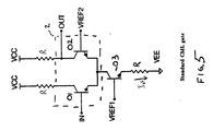
- FIG. 1 illustrates a standard ECL gate. It comprises differential pair 2 (which includes N-type bipolar transistors 01 and 02) and source follower stage 4. N-type bipolar transistors 04 and 05 are connected together so as to form the output of the gate.
- the gate's power dissipation is controlled by the VREF1 signal (VREF1 being a voltage). If transistor 03 is kept out of saturation during its operation, then current Ics (through resistor R connected to the emitter of transistor 03) is equal to (VREFl-VBE)/R.
- the VREF1 voltage controls the output voltage swing of the gate. It can be seen that the difference between the high and the low output levels of this gate is Ics*R and that this is a voltage drop across the pull-up resistor of the differential pair.
- the input trip point of this gate is set up by a VREF2 signal voltage between power supply voltage VCC and the voltage at the base of transistor 02. If the input of this ECL gate (node IN) is driven by the signal from the output of another ECL gate similar to this gate, then VREF2 has to be set at the midpoint of this output voltage swing to achieve maximum signal margin and performance. If VREF1 and VREF2 are kept at constant levels, then voltage drops on the VCC and VEE power lines will invalidate both voltage references.
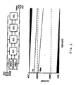
- Figure 2 illustrates the physical layout of VCC and VEE power supply pads on a chip and an associated graph.
- the pads are near each other.
- the band-gap reference circuit which produces voltages VREF1 and VREF2 is placed near the power pads and blocks of ECL circuits are placed at increasing distances away from the power pads. Resistances in the power lines are shown modeled as resistors R.
- the graph in figure 2 illustrates selected voltages vs. distance.
- the X axis gives the distance from the power pads of the corresponding ECL circuit shown above it and the Y axis shows the voltage of major signals in the ECL gates.
- the voltage drops along the VCC and VEE power lines are shown here in the graph as the dark regions.
- the ECL circuit at the end of the power lines suffers the most voltage drop.
- VREF1 and VREF2 are referenced to the power pads, they are at a constant level regardless of how far they are away from the pads. However, the current reproduced by VREF1 at the local ECL circuit is not constant. This will effect the low output voltage of ECL gates along the power lines.
- the high output of the ECL gate is also lowered by voltage drops in the VCC line. These effects severely degrade the signal margin. If the voltage drops in the power line are greater than one half of output voltage swing, this will probably result in complete chip operation failure.
- Figure 3 illustrates an example of a SRAM which is designed to fit in a standard JDEC package.
- Figure 3 also illustrates a corresponding graph of selected voltages vs. distance, a similar type of plot to that illustrated in figure 2. It has the power pads at opposite ends of the chip. The effects of the power line voltage drops are almost the same except that now the signal voltage swings are larger and may cause catastrophic failure due to the forward biasing of the next ECL stages which are receiving output signals.
- Figure 4 illustrates multiple (two) band-gap reference circuits in a configuration similar to that shown in figures 2 and 3.
- Figure 4 additionally illustrates a corresponding graph of selected voltages vs. distance.
- Two band-gap circuits are placed at each end of the package. Large layout areas are required for this scheme. Additionally, the critical location of these reference circuits reduce the effectiveness of the scheme.
- the ECL circuits farthest from the reference circuits still suffer signal degredations and still depend on how much power line voltages have dropped at their location. A similar problem arises in other circuits involving current mode logic, CML, gates.
- Figure 5 illustrates a standard CML gate comprising differential pair 2 comprising transistors 01 and 02 connected to transistor 03.
- the foregoing objects of the invention are accomplished by establishing reference voltages which are defined with respect to local power supply levels.
- the local supply levels are established through the use of a network of reference current sources.
- the reference current sources can be routed across the chip without having to give special consideration to power supply fluctuations.
- the current sources serve as inputs to analog drivers which generate the reference voltages with the respect to the local power supply levels.
- the semiconductor chip on which the invention is embodied uses a global band-gap reference circuit that operates in conjunction with current source feed back implemented with a PMOS current mirror. BiCMOS Op Amps are used as the analog drivers.
- the analog drivers convert band-gap reference outputs to the required levels and provide low impedance sources to ECL circuits for the chip.
- FIG. 7 illustrated a preferred embodiment of the invention together with a graph of selected voltages vs. chip distance.
- Each ECL circuit block has its own reference circuit VREGEN.
- the ECL circuits receive not the voltages, but the current references from a reference current generator.
- a reference current generator converts the voltage from a band-gap reference circuit to currents before sending the signal to remote locations such as ECL gates distributed on a chip. At these locations, the reference current will be converted to voltage to provide a correct reference voltage for a local circuit such as a local ECL gate.
- the invention thus substantially eliminates the previously discussed problem of voltage drop in power supply lines leading to each ECL block. As shown in the graph, VREF1 and VREF2 are correctly referenced to the local power supply levels. Maximum signal margin is restored because the I/O signals inside each ECL block are now at correct levels. Notice that the signals are only offset from block to block.
- the trip point reference level should be sent to the receiving circuit from the sender to improve the signal margin.
- Level shifter circuits at both sender or receiver will provide an effective communication but it will add some complicated circuitry.
- the simplest technique improves the ground line. Reducing the voltage drops of the VCC line (widening the VCC power line) in the ECL circuit will effectively improve the signal margin by the same amount.
- Figure 8 illustrates an embodiment of the invention similar to that shown in Figure 7.
- the VCC power line voltage drop has been minimized through allocation of more area for it in a circuit layout.
- the invention allows the circuit to tolerate the voltage drops on the VEE line much more than the standard reference techniques. If the VCC power line voltage is as shown, then all ECL I/O (input/output) signals from all blocks will be aligned.
- the invention makes the physical location of the band-gap and the current generator with respect to power pads and circuit blocks noncritical.
- a key component of the network of the invention is a BiCMOS band-gap circuit which is insensitive to the power supply variations.
- This band-gap circuit was disclosed in Serial Number 07/161,694, filed February 29, 1988.
- figure 9 illustrates a standard band-gap reference circuit.
- a current source is connected to the base of N-type bipolar transistor Q2 and the collector of N-type bipolar transistor Q1.
- the base of Q1 is connected to the collector of n-type transistor nQ3 and the bases of transistor nQ3 and transistor Q3 are connected together.
- Resistors are illustrated with their relative values displayed alongside. Voltages are displayed between arrowheads. The output of the circuit results in a reference voltage VREF.
- the reference output VREF is equal to the sum of VBE and k*delta VBE (k being the denominator of the resistor connected to the collector of transistor nQ3).
- Transistor Q1 is used as a negative feedback amplifier to keep the VREF at nearly equal to the band-gap voltage of silicon (about 1.25 volt) for maximum temperature stability.
- the variation of the load current Ia (from the current source) of this circuit has a direct effect on the VREF output.
- One of the main causes of the Ia current variation is the power supply fluctuation.
- the band-gap circuit of the invention keeps the current Ia as stable as possible. There are many existing circuit techniques to generate a stable current source for this purpose, but they are often unreliable, complicated and required a large layout area. For example, one of the most common design techniques is using another band-gap to generate the Ia current.
- FIG. 10 illustrates the BiCMOS band-gap circuit used in the invention. Unlike standard band-gap circuits, this circuit is simple and does not require a second band-gap circuit to generate the Ia current.
- This circuit uses its own band-gap output to generate a load current. This is accomplished by using the P-channel MOS transistors, P1 and P2, to mirror the current I which is generated by the output voltage VREF, from transistor Q4 through resistor R, and to the load of a feed back amplifier, transistor Q1.
- a stable voltage output VREF will provide a steady load current and vice versa by the self-feed-back.
- a start-up circuit is required to keep the circuit out of zero current mode (which produces zero feed back) due to the self-feed-back. Once the reference output is at a correct level, the start-up circuit is no longer needed and should be electrically disconnected to avoid possible ill effects. Notice that the currents flowing in the branches are kept equal for maximum tracking ability.
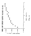
- Figure 11 shows the output of the invention's band-gap circuit versus a VCC voltage from 3 to 7 volts. Fourteen milivolts of output variation was seen across the entire range (.35%), but the circuit operates much better in a VCC range from 4 to 7 volts. The output only varied 5 milivolts in this range (.16%).
- FIG. 12 illustrates the reference current to voltage conversion circuit of the invention.
- This circuit is used at each local location of an ECL circuit block.
- the global band-gap voltage VREF is converted to a reference current IREF and then routed to a remote ECL circuit block.
- the IREF current is mirrored by P-channel transistors 13 and 15 and passed through bipolar transistor Q20 and resistor R to regenerate the VREF level that corresponds to the local VEE voltage level.
- the output from this circuit can be directly connected to ECL circuits (as shown) or can be connected to an operational amplifier (Op Amp) to provide greater current handling capability or more flexibility to regenerate different voltage reference levels.
- the VREF signal is taken from the emitter of transistor Q10 which is connected to P-channel transistor 15 and bipolar transistor Q20.
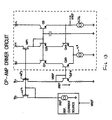
- FIG. 13 illustrates the Op Amp driver circuit discussed above.
- the Op Amp driver is shown inside the dashed box.
- the Op Amp is connected in a unity gain configuration to produce at its output the same voltage level connected to its input. It uses a P-channel current source NP1 for the load to improve the gain of the differential stage comprising bipolar transistors Q30, Q40 and current source CS.
- the cascode transistors Q11 and Q21 are used to minimize the input offset which might be caused by the difference of the VCE voltage between transistors Q30 and Q40.
- the output from the Op Amp driver circuit is taken from the emitter of transistor Q5.
- Other circuitry for implementing the connection of the Op Amp to the rest of the scheme comprises gate connected P-channel transistors MP2 and MP3. Diode configured transistor Q50 is connected to P-channel transistor MP3 and generates a reference current IREF.
- the network was implemented in a 1meg BiCMOS SRAM.
- the block diagram of the network is shown in figure 14.
- Power supply pads are at the opposite side of the chip.
- the global band-gap is placed near VCC power pad.
- Reference current is routed to the other side of the network and regenerated at local ECL circuit locations.
- BiCMoS circuits are used for global communications in this SRAM.
- the characteristics of the foregoing network include minimized power supply drop effects, maximized ECL signal margin, and improved ECL circuit performance of a VLSI BiCMOS ECL chip.
- bipolar transistor may substituted for field-effect transistors and vice-versa.
- P-type transistors may be substituted for n-type transistors and vice-versa.
- N-channel transistors may be substituted for P-channel transistors and vice-versa. It is contemplated that all such changes and additions are within the spirit and true scope of the invention as claimed below. Accordingly, the invention is intended to be limited only by the scope of the appended claims.
Landscapes
- Engineering & Computer Science (AREA)
- Microelectronics & Electronic Packaging (AREA)
- Physics & Mathematics (AREA)
- Power Engineering (AREA)
- Nonlinear Science (AREA)
- Electromagnetism (AREA)
- General Physics & Mathematics (AREA)
- Radar, Positioning & Navigation (AREA)
- Automation & Control Theory (AREA)
- Computer Hardware Design (AREA)
- Logic Circuits (AREA)
- Control Of Electrical Variables (AREA)
Applications Claiming Priority (2)
| Application Number | Priority Date | Filing Date | Title |
|---|---|---|---|
| US310800 | 1989-02-14 | ||
| US07/310,800 US5001362A (en) | 1989-02-14 | 1989-02-14 | BiCMOS reference network |
Publications (3)
| Publication Number | Publication Date |
|---|---|
| EP0383095A2 true EP0383095A2 (de) | 1990-08-22 |
| EP0383095A3 EP0383095A3 (de) | 1991-12-27 |
| EP0383095B1 EP0383095B1 (de) | 1995-06-21 |
Family
ID=23204167
Family Applications (1)
| Application Number | Title | Priority Date | Filing Date |
|---|---|---|---|
| EP90101884A Expired - Lifetime EP0383095B1 (de) | 1989-02-14 | 1990-01-31 | BICMOS-Referenznetzwerk |
Country Status (5)
| Country | Link |
|---|---|
| US (1) | US5001362A (de) |
| EP (1) | EP0383095B1 (de) |
| JP (1) | JP2912660B2 (de) |
| KR (1) | KR900013520A (de) |
| DE (1) | DE69020178T2 (de) |
Cited By (2)
| Publication number | Priority date | Publication date | Assignee | Title |
|---|---|---|---|---|
| EP0491302A3 (en) * | 1990-12-17 | 1993-01-27 | Hewlett-Packard Company | Bicmos voltage generator |
| DE10035414A1 (de) * | 2000-07-20 | 2002-02-07 | Infineon Technologies Ag | Integrierter Schaltkreis mit Referenzstromversorgung |
Families Citing this family (12)
| Publication number | Priority date | Publication date | Assignee | Title |
|---|---|---|---|---|
| US5309040A (en) * | 1989-11-07 | 1994-05-03 | Fujitsu Limited | Voltage reducing circuit |
| JP2683948B2 (ja) * | 1990-06-19 | 1997-12-03 | 三菱電機株式会社 | 半導体集積回路 |
| US5291455A (en) * | 1992-05-08 | 1994-03-01 | Motorola, Inc. | Memory having distributed reference and bias voltages |
| JPH05327463A (ja) * | 1992-05-15 | 1993-12-10 | Mitsubishi Electric Corp | 出力回路 |
| US5306964A (en) * | 1993-02-22 | 1994-04-26 | Intel Corporation | Reference generator circuit for BiCMOS ECL gate employing PMOS load devices |
| KR100316834B1 (ko) * | 1993-12-27 | 2002-04-24 | 가나이 쓰도무 | 기준전류발생회로,정전류발생회로및그것을사용한장치 |
| US5760639A (en) * | 1996-03-04 | 1998-06-02 | Motorola, Inc. | Voltage and current reference circuit with a low temperature coefficient |
| US6710586B2 (en) * | 2001-11-22 | 2004-03-23 | Denso Corporation | Band gap reference voltage circuit for outputting constant output voltage |
| US7321225B2 (en) * | 2004-03-31 | 2008-01-22 | Silicon Laboratories Inc. | Voltage reference generator circuit using low-beta effect of a CMOS bipolar transistor |
| US7224210B2 (en) * | 2004-06-25 | 2007-05-29 | Silicon Laboratories Inc. | Voltage reference generator circuit subtracting CTAT current from PTAT current |
| US7180310B2 (en) * | 2004-10-27 | 2007-02-20 | Advantest Corporation | Amplitude varying driver circuit and test apparatus |
| US7268720B1 (en) * | 2006-06-30 | 2007-09-11 | Analog Devices, Inc. | Converter networks for generation of MDAC reference signals |
Family Cites Families (10)
| Publication number | Priority date | Publication date | Assignee | Title |
|---|---|---|---|---|
| JPS60953B2 (ja) * | 1977-12-30 | 1985-01-11 | 富士通株式会社 | 半導体集積回路装置 |
| JPS5816396A (ja) * | 1981-07-20 | 1983-01-31 | パイオニア株式会社 | 電圧−電流変換回路 |
| JPS59212780A (ja) * | 1983-05-18 | 1984-12-01 | Toshiba Corp | レベル検出回路 |
| JPS6093532A (ja) * | 1983-10-27 | 1985-05-25 | Matsushita Electric Ind Co Ltd | 基準電圧回路 |
| US4588941A (en) * | 1985-02-11 | 1986-05-13 | At&T Bell Laboratories | Cascode CMOS bandgap reference |
| US4618816A (en) * | 1985-08-22 | 1986-10-21 | National Semiconductor Corporation | CMOS ΔVBE bias current generator |
| JPS62230222A (ja) * | 1986-03-31 | 1987-10-08 | Toshiba Corp | 入力回路 |
| IT1190325B (it) * | 1986-04-18 | 1988-02-16 | Sgs Microelettronica Spa | Circuito di polarizzazione per dispositivi integrati in tecnologia mos,particolarmente di tipo misto digitale-analogico |
| IT1201848B (it) * | 1986-10-02 | 1989-02-02 | Sgs Microelettronica Spa | Circuito di interfaccia logica ad alta stabilita' e bassa corrente di riposo |
| US4742292A (en) * | 1987-03-06 | 1988-05-03 | International Business Machines Corp. | CMOS Precision voltage reference generator |
-
1989
- 1989-02-14 US US07/310,800 patent/US5001362A/en not_active Expired - Lifetime
-
1990
- 1990-01-31 EP EP90101884A patent/EP0383095B1/de not_active Expired - Lifetime
- 1990-01-31 DE DE69020178T patent/DE69020178T2/de not_active Expired - Fee Related
- 1990-02-14 JP JP2033618A patent/JP2912660B2/ja not_active Expired - Lifetime
- 1990-02-14 KR KR1019900001795A patent/KR900013520A/ko not_active Abandoned
Cited By (2)
| Publication number | Priority date | Publication date | Assignee | Title |
|---|---|---|---|---|
| EP0491302A3 (en) * | 1990-12-17 | 1993-01-27 | Hewlett-Packard Company | Bicmos voltage generator |
| DE10035414A1 (de) * | 2000-07-20 | 2002-02-07 | Infineon Technologies Ag | Integrierter Schaltkreis mit Referenzstromversorgung |
Also Published As
| Publication number | Publication date |
|---|---|
| JP2912660B2 (ja) | 1999-06-28 |
| KR900013520A (ko) | 1990-09-06 |
| DE69020178D1 (de) | 1995-07-27 |
| EP0383095B1 (de) | 1995-06-21 |
| EP0383095A3 (de) | 1991-12-27 |
| US5001362A (en) | 1991-03-19 |
| JPH0315916A (ja) | 1991-01-24 |
| DE69020178T2 (de) | 1996-02-08 |
Similar Documents
| Publication | Publication Date | Title |
|---|---|---|
| KR100368982B1 (ko) | 씨모스 정전류 레퍼런스 회로 | |
| EP0905902B1 (de) | Konstantstrom-CMOS-Ausgangstreiberschaltung mit Dual-Gate-Transistoren | |
| US7259543B2 (en) | Sub-1V bandgap reference circuit | |
| EP0383095B1 (de) | BICMOS-Referenznetzwerk | |
| US5568045A (en) | Reference voltage generator of a band-gap regulator type used in CMOS transistor circuit | |
| EP0305098A2 (de) | CMOS/ECL Konverter-Ausgangspufferschaltung | |
| EP0590818A2 (de) | ECL zu BICMOS/CMOS-Umsetzer | |
| WO1998048334A9 (en) | Precision bandgap reference circuit | |
| US5563502A (en) | Constant voltage generation circuit | |
| US4453121A (en) | Reference voltage generator | |
| US4677368A (en) | Precision thermal current source | |
| EP0413228A2 (de) | Umsetzschaltung von TTL nach ECL/CML | |
| US4855624A (en) | Low-power bipolar-CMOS interface circuit | |
| CN115454190A (zh) | 一种lvds驱动电路 | |
| US5120994A (en) | Bicmos voltage generator | |
| EP0264563A1 (de) | Spannungsregler mit Präzisionsthermostromquelle | |
| US4100478A (en) | Monolithic regulator for CML devices | |
| US5225716A (en) | Semiconductor integrated circuit having means for suppressing a variation in a threshold level due to temperature variation | |
| KR20000009310A (ko) | 저전압 동작용 바이어스 전류회로 | |
| EP0326955B1 (de) | BICMOS-Spannungsreferenzgenerator | |
| JP3104509B2 (ja) | 定電流発生回路及びそれを用いた装置 | |
| US6703864B2 (en) | Buffer circuit | |
| KR950008792B1 (ko) | 온도변동으로 인한 임계치 레벨의 변화를 억제하는 수단을 갖는 반도체 집적회로 | |
| TWI915886B (zh) | 產生與溫度無關參考電壓的裝置及方法 | |
| US20250334990A1 (en) | Device and Method for Generating a Temperature-Independent Reference Voltage |
Legal Events
| Date | Code | Title | Description |
|---|---|---|---|
| PUAI | Public reference made under article 153(3) epc to a published international application that has entered the european phase |
Free format text: ORIGINAL CODE: 0009012 |
|
| AK | Designated contracting states |
Kind code of ref document: A2 Designated state(s): DE FR GB IT NL |
|
| PUAL | Search report despatched |
Free format text: ORIGINAL CODE: 0009013 |
|
| AK | Designated contracting states |
Kind code of ref document: A3 Designated state(s): DE FR GB IT NL |
|
| 17P | Request for examination filed |
Effective date: 19920525 |
|
| 17Q | First examination report despatched |
Effective date: 19940126 |
|
| GRAA | (expected) grant |
Free format text: ORIGINAL CODE: 0009210 |
|
| AK | Designated contracting states |
Kind code of ref document: B1 Designated state(s): DE FR GB IT NL |
|
| PG25 | Lapsed in a contracting state [announced via postgrant information from national office to epo] |
Ref country code: NL Free format text: LAPSE BECAUSE OF FAILURE TO SUBMIT A TRANSLATION OF THE DESCRIPTION OR TO PAY THE FEE WITHIN THE PRESCRIBED TIME-LIMIT Effective date: 19950621 |
|
| REF | Corresponds to: |
Ref document number: 69020178 Country of ref document: DE Date of ref document: 19950727 |
|
| ITF | It: translation for a ep patent filed | ||
| ET | Fr: translation filed | ||
| NLV1 | Nl: lapsed or annulled due to failure to fulfill the requirements of art. 29p and 29m of the patents act | ||
| PLBE | No opposition filed within time limit |
Free format text: ORIGINAL CODE: 0009261 |
|
| STAA | Information on the status of an ep patent application or granted ep patent |
Free format text: STATUS: NO OPPOSITION FILED WITHIN TIME LIMIT |
|
| 26N | No opposition filed | ||
| REG | Reference to a national code |
Ref country code: GB Ref legal event code: IF02 |
|
| PGFP | Annual fee paid to national office [announced via postgrant information from national office to epo] |
Ref country code: GB Payment date: 20071212 Year of fee payment: 19 |
|
| PGFP | Annual fee paid to national office [announced via postgrant information from national office to epo] |
Ref country code: DE Payment date: 20080131 Year of fee payment: 19 Ref country code: IT Payment date: 20080116 Year of fee payment: 19 |
|
| PGFP | Annual fee paid to national office [announced via postgrant information from national office to epo] |
Ref country code: FR Payment date: 20080107 Year of fee payment: 19 |
|
| GBPC | Gb: european patent ceased through non-payment of renewal fee |
Effective date: 20090131 |
|
| PG25 | Lapsed in a contracting state [announced via postgrant information from national office to epo] |
Ref country code: DE Free format text: LAPSE BECAUSE OF NON-PAYMENT OF DUE FEES Effective date: 20090801 |
|
| REG | Reference to a national code |
Ref country code: FR Ref legal event code: ST Effective date: 20091030 |
|
| PG25 | Lapsed in a contracting state [announced via postgrant information from national office to epo] |
Ref country code: GB Free format text: LAPSE BECAUSE OF NON-PAYMENT OF DUE FEES Effective date: 20090131 |
|
| PG25 | Lapsed in a contracting state [announced via postgrant information from national office to epo] |
Ref country code: FR Free format text: LAPSE BECAUSE OF NON-PAYMENT OF DUE FEES Effective date: 20090202 |
|
| PG25 | Lapsed in a contracting state [announced via postgrant information from national office to epo] |
Ref country code: IT Free format text: LAPSE BECAUSE OF NON-PAYMENT OF DUE FEES Effective date: 20090131 |