EP0386574A1 - CMOS- und Bipolar-Herstellungsverfahren durch selektives, epitaxiales Aufwachsen zur Dimensionierung unterhalb von 0,5 Mikron - Google Patents
CMOS- und Bipolar-Herstellungsverfahren durch selektives, epitaxiales Aufwachsen zur Dimensionierung unterhalb von 0,5 Mikron Download PDFInfo
- Publication number
- EP0386574A1 EP0386574A1 EP90103678A EP90103678A EP0386574A1 EP 0386574 A1 EP0386574 A1 EP 0386574A1 EP 90103678 A EP90103678 A EP 90103678A EP 90103678 A EP90103678 A EP 90103678A EP 0386574 A1 EP0386574 A1 EP 0386574A1
- Authority
- EP
- European Patent Office
- Prior art keywords
- substrate
- region
- epitaxial
- conductivity type
- regions
- Prior art date
- Legal status (The legal status is an assumption and is not a legal conclusion. Google has not performed a legal analysis and makes no representation as to the accuracy of the status listed.)
- Withdrawn
Links
Images
Classifications
-
- H—ELECTRICITY
- H10—SEMICONDUCTOR DEVICES; ELECTRIC SOLID-STATE DEVICES NOT OTHERWISE PROVIDED FOR
- H10D—INORGANIC ELECTRIC SEMICONDUCTOR DEVICES
- H10D62/00—Semiconductor bodies, or regions thereof, of devices having potential barriers
- H10D62/10—Shapes, relative sizes or dispositions of the regions of the semiconductor bodies; Shapes of the semiconductor bodies
- H10D62/113—Isolations within a component, i.e. internal isolations
- H10D62/115—Dielectric isolations, e.g. air gaps
-
- H—ELECTRICITY
- H10—SEMICONDUCTOR DEVICES; ELECTRIC SOLID-STATE DEVICES NOT OTHERWISE PROVIDED FOR
- H10D—INORGANIC ELECTRIC SEMICONDUCTOR DEVICES
- H10D62/00—Semiconductor bodies, or regions thereof, of devices having potential barriers
- H10D62/10—Shapes, relative sizes or dispositions of the regions of the semiconductor bodies; Shapes of the semiconductor bodies
- H10D62/13—Semiconductor regions connected to electrodes carrying current to be rectified, amplified or switched, e.g. source or drain regions
- H10D62/137—Collector regions of BJTs
-
- H—ELECTRICITY
- H10—SEMICONDUCTOR DEVICES; ELECTRIC SOLID-STATE DEVICES NOT OTHERWISE PROVIDED FOR
- H10D—INORGANIC ELECTRIC SEMICONDUCTOR DEVICES
- H10D84/00—Integrated devices formed in or on semiconductor substrates that comprise only semiconducting layers, e.g. on Si wafers or on GaAs-on-Si wafers
- H10D84/01—Manufacture or treatment
- H10D84/0107—Integrating at least one component covered by H10D12/00 or H10D30/00 with at least one component covered by H10D8/00, H10D10/00 or H10D18/00, e.g. integrating IGFETs with BJTs
- H10D84/0109—Integrating at least one component covered by H10D12/00 or H10D30/00 with at least one component covered by H10D8/00, H10D10/00 or H10D18/00, e.g. integrating IGFETs with BJTs the at least one component covered by H10D12/00 or H10D30/00 being a MOS device
-
- H—ELECTRICITY
- H10—SEMICONDUCTOR DEVICES; ELECTRIC SOLID-STATE DEVICES NOT OTHERWISE PROVIDED FOR
- H10D—INORGANIC ELECTRIC SEMICONDUCTOR DEVICES
- H10D84/00—Integrated devices formed in or on semiconductor substrates that comprise only semiconducting layers, e.g. on Si wafers or on GaAs-on-Si wafers
- H10D84/01—Manufacture or treatment
- H10D84/02—Manufacture or treatment characterised by using material-based technologies
- H10D84/03—Manufacture or treatment characterised by using material-based technologies using Group IV technology, e.g. silicon technology or silicon-carbide [SiC] technology
- H10D84/038—Manufacture or treatment characterised by using material-based technologies using Group IV technology, e.g. silicon technology or silicon-carbide [SiC] technology using silicon technology, e.g. SiGe
-
- H—ELECTRICITY
- H10—SEMICONDUCTOR DEVICES; ELECTRIC SOLID-STATE DEVICES NOT OTHERWISE PROVIDED FOR
- H10P—GENERIC PROCESSES OR APPARATUS FOR THE MANUFACTURE OR TREATMENT OF DEVICES COVERED BY CLASS H10
- H10P14/00—Formation of materials, e.g. in the shape of layers or pillars
- H10P14/20—Formation of materials, e.g. in the shape of layers or pillars of semiconductor materials
- H10P14/24—Formation of materials, e.g. in the shape of layers or pillars of semiconductor materials using chemical vapour deposition [CVD]
-
- H—ELECTRICITY
- H10—SEMICONDUCTOR DEVICES; ELECTRIC SOLID-STATE DEVICES NOT OTHERWISE PROVIDED FOR
- H10P—GENERIC PROCESSES OR APPARATUS FOR THE MANUFACTURE OR TREATMENT OF DEVICES COVERED BY CLASS H10
- H10P14/00—Formation of materials, e.g. in the shape of layers or pillars
- H10P14/20—Formation of materials, e.g. in the shape of layers or pillars of semiconductor materials
- H10P14/27—Formation of materials, e.g. in the shape of layers or pillars of semiconductor materials using selective deposition, e.g. simultaneous growth of monocrystalline and non-monocrystalline semiconductor materials
- H10P14/271—Formation of materials, e.g. in the shape of layers or pillars of semiconductor materials using selective deposition, e.g. simultaneous growth of monocrystalline and non-monocrystalline semiconductor materials characterised by the preparation of substrate for selective deposition
-
- H—ELECTRICITY
- H10—SEMICONDUCTOR DEVICES; ELECTRIC SOLID-STATE DEVICES NOT OTHERWISE PROVIDED FOR
- H10P—GENERIC PROCESSES OR APPARATUS FOR THE MANUFACTURE OR TREATMENT OF DEVICES COVERED BY CLASS H10
- H10P14/00—Formation of materials, e.g. in the shape of layers or pillars
- H10P14/20—Formation of materials, e.g. in the shape of layers or pillars of semiconductor materials
- H10P14/29—Formation of materials, e.g. in the shape of layers or pillars of semiconductor materials characterised by the substrates
- H10P14/2901—Materials
- H10P14/2902—Materials being Group IVA materials
- H10P14/2905—Silicon, silicon germanium or germanium
-
- H—ELECTRICITY
- H10—SEMICONDUCTOR DEVICES; ELECTRIC SOLID-STATE DEVICES NOT OTHERWISE PROVIDED FOR
- H10P—GENERIC PROCESSES OR APPARATUS FOR THE MANUFACTURE OR TREATMENT OF DEVICES COVERED BY CLASS H10
- H10P14/00—Formation of materials, e.g. in the shape of layers or pillars
- H10P14/20—Formation of materials, e.g. in the shape of layers or pillars of semiconductor materials
- H10P14/34—Deposited materials, e.g. layers
- H10P14/3402—Deposited materials, e.g. layers characterised by the chemical composition
- H10P14/3404—Deposited materials, e.g. layers characterised by the chemical composition being Group IVA materials
- H10P14/3411—Silicon, silicon germanium or germanium
-
- H—ELECTRICITY
- H10—SEMICONDUCTOR DEVICES; ELECTRIC SOLID-STATE DEVICES NOT OTHERWISE PROVIDED FOR
- H10W—GENERIC PACKAGES, INTERCONNECTIONS, CONNECTORS OR OTHER CONSTRUCTIONAL DETAILS OF DEVICES COVERED BY CLASS H10
- H10W10/00—Isolation regions in semiconductor bodies between components of integrated devices
- H10W10/01—Manufacture or treatment
- H10W10/011—Manufacture or treatment of isolation regions comprising dielectric materials
- H10W10/018—Manufacture or treatment of isolation regions comprising dielectric materials using selective deposition of crystalline silicon, e.g. using epitaxial growth of silicon
-
- H—ELECTRICITY
- H10—SEMICONDUCTOR DEVICES; ELECTRIC SOLID-STATE DEVICES NOT OTHERWISE PROVIDED FOR
- H10W—GENERIC PACKAGES, INTERCONNECTIONS, CONNECTORS OR OTHER CONSTRUCTIONAL DETAILS OF DEVICES COVERED BY CLASS H10
- H10W10/00—Isolation regions in semiconductor bodies between components of integrated devices
- H10W10/10—Isolation regions comprising dielectric materials
-
- H—ELECTRICITY
- H10—SEMICONDUCTOR DEVICES; ELECTRIC SOLID-STATE DEVICES NOT OTHERWISE PROVIDED FOR
- H10W—GENERIC PACKAGES, INTERCONNECTIONS, CONNECTORS OR OTHER CONSTRUCTIONAL DETAILS OF DEVICES COVERED BY CLASS H10
- H10W15/00—Highly-doped buried regions of integrated devices
-
- H—ELECTRICITY
- H10—SEMICONDUCTOR DEVICES; ELECTRIC SOLID-STATE DEVICES NOT OTHERWISE PROVIDED FOR
- H10W—GENERIC PACKAGES, INTERCONNECTIONS, CONNECTORS OR OTHER CONSTRUCTIONAL DETAILS OF DEVICES COVERED BY CLASS H10
- H10W15/00—Highly-doped buried regions of integrated devices
- H10W15/01—Manufacture or treatment
-
- Y—GENERAL TAGGING OF NEW TECHNOLOGICAL DEVELOPMENTS; GENERAL TAGGING OF CROSS-SECTIONAL TECHNOLOGIES SPANNING OVER SEVERAL SECTIONS OF THE IPC; TECHNICAL SUBJECTS COVERED BY FORMER USPC CROSS-REFERENCE ART COLLECTIONS [XRACs] AND DIGESTS
- Y10—TECHNICAL SUBJECTS COVERED BY FORMER USPC
- Y10S—TECHNICAL SUBJECTS COVERED BY FORMER USPC CROSS-REFERENCE ART COLLECTIONS [XRACs] AND DIGESTS
- Y10S148/00—Metal treatment
- Y10S148/011—Bipolar transistors
-
- Y—GENERAL TAGGING OF NEW TECHNOLOGICAL DEVELOPMENTS; GENERAL TAGGING OF CROSS-SECTIONAL TECHNOLOGIES SPANNING OVER SEVERAL SECTIONS OF THE IPC; TECHNICAL SUBJECTS COVERED BY FORMER USPC CROSS-REFERENCE ART COLLECTIONS [XRACs] AND DIGESTS
- Y10—TECHNICAL SUBJECTS COVERED BY FORMER USPC
- Y10S—TECHNICAL SUBJECTS COVERED BY FORMER USPC CROSS-REFERENCE ART COLLECTIONS [XRACs] AND DIGESTS
- Y10S148/00—Metal treatment
- Y10S148/026—Deposition thru hole in mask
-
- Y—GENERAL TAGGING OF NEW TECHNOLOGICAL DEVELOPMENTS; GENERAL TAGGING OF CROSS-SECTIONAL TECHNOLOGIES SPANNING OVER SEVERAL SECTIONS OF THE IPC; TECHNICAL SUBJECTS COVERED BY FORMER USPC CROSS-REFERENCE ART COLLECTIONS [XRACs] AND DIGESTS
- Y10—TECHNICAL SUBJECTS COVERED BY FORMER USPC
- Y10S—TECHNICAL SUBJECTS COVERED BY FORMER USPC CROSS-REFERENCE ART COLLECTIONS [XRACs] AND DIGESTS
- Y10S148/00—Metal treatment
- Y10S148/031—Diffusion at an edge
Definitions
- This invention relates to semiconductor device fabrication methods and, more particularly, to a CMOS and bipolar fabrication process using selective epitaxial growth.
- LOCOS isoplanar
- latch-up considerations in CMOS prevent putting opposite type devices in very close proximity unless more complex processing is added.
- CMOS isolation Current state-of-the-art one to two micron level approaches to CMOS isolation include the use of trenches and epitaxial buried layers.
- Trench isolation has the disadvantage of requiring very complex and costly processing, and it requires some other type of oxide isolation for the majority of the chip's surface (typically LOCOS).
- MOS transistors cannot be set directly against a trench wall because of degradation of device characteristics, thus increasing the area consumed by one transistor.
- Epitaxial buried layer isolation while somewhat effective, still has a lower limit of approximately 2.5 micrometers for PMOS to NMOS spacing due to junction breakdown and punch-through.
- CMOS isolation by selective epitaxial growth has been proposed.
- SEG selective epitaxial growth
- a silicon substrate is etched to form openings in the substrate, and insulators are formed on the side walls of the openings. Thereafter, the substrate is masked and doped to a chosen conductivity type, and an epitaxial layer is grown to fill the openings. A final LOCOS isolation then is performed.
- the disadvantages of this method are the requirement of etching into the silicon surface and the requirement of LOCOS isolation with the inherent bird's beak encroachment.
- a silicon dioxide layer is formed over a silicon substrate, and the silicon dioxide layer is etched for forming openings extending to the substrate.
- the openings are filled by growing epitaxial layers having a selected conductivity type (e.g. , N-type) on the substrate.
- a selected conductivity type e.g. , N-type
- the wells then are covered by thin thermal oxide layers to protect them from later process steps.
- the process then is repeated to form wells having an opposite conductivity type (e.g. , P-type). Thereafter, the thin oxide layers over the previously formed wells are stripped.
- this method does not require LOCOS isolation, it must be implemented with multiple SEG steps.
- the present invention is directed to a relatively simple front-end process for isolating semiconductor devices wherein the process requires only one SEG step, provides twin buried layers which may be controlled independently, and uses a simple thermal oxidation step for isolation between devices. Active P and N regions are separately formed with self-aligned implants, and with fewer masking steps than conventional techniques. Unlike devices isolated by trenches, the isolation width can be any dimension above the resolution of the patterning tool for MOS devices of the same type, and the resolution of the patterning tool plus one registration tolerance for opposite type devices. Thus, if 0.5 micron is the resolution of the patterning tool, 0.5 micron isolation between same-type devices is achieved, and the process is scalable well into the submicron region. At submicron levels, no other presently known technique can provide a minimum device pitch of twice the resolution of the patterning tool with a planarized surface without substantially more complex processing.
- the method according to the present invention minimizes collector-base capacitance through the use of oxide isolated collectors while also using a bipolar buried layer, whereas the independent P+ and N+ buried layers minimize the collector-to-substrate capacitance. Punch-through problems are eliminated because of full oxide isolation between devices. Finally, the front end of this process is compatible with the most advanced CMOS and bipolar backend device fabrication processes, such as silicided source-drain-gate areas and contacts/posts overlapping on field oxide for MOS devices, and a poly-emitter or a poly-base and emitter for bipolar devices.
- a silicon dioxide layer is formed over a silicon substrate.
- the silicon dioxide layer is etched for forming separate collector and base/emitter regions for a bipolar device, and PMOS and NMOS regions for corresponding PMOS and NMOS devices. Buried layer implants are performed, and an epitaxial layer is grown over the exposed portions of the silicon substrate.
- the silicon dioxide walls between the devices provide full dielectric isolation between the devices as well as between the collector and base/emitter regions of the bipolar device. Nonetheless, the oxide wall between the collector and base/emitter of the bipolar device is sufficiently small to allow the buried layer implants to join under the wall for forming a conventional buried layer for the bipolar device. Because of the oxide walls, the minimum distance between devices may be 0.5 microns or less.
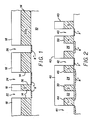
- Figs. 1-5 illustrate the method according to the present invention for forming CMOS and bipolar devices using selective epitaxial growth.
- Fig. 1 shows one embodiment of a silicon substrate 10 after undergoing preliminary processing according to the present invention.
- the substrate material is P-type 100 with 100 flat orientation and resistivity greater than 10 ohm-cm.
- the flat orientation is preferable to achieve the best selectively grown epitaxial layers with minimal faceting and stress.
- the orientation also helps to reduce fixed charges along the vertical sidewalls of the oxide isolation regions.
- a silicon dioxide layer 14 is thermally grown to a thickness of from approximately 0.8 to 1.5 microns by placing substrate 10 in an oxygen environment at 1000°C for approximately 300 minutes, making certain that the oxidation cycle includes conventional denuded zone formation steps. This ensures that the selectively grown epitaxial layer will not have stacking faults along the horizontal surface.
- a photoresist layer 18 is deposited and developed for forming the openings shown. The portions of silicon dioxide layer 14 beneath the openings in photoresist layer 18 then are etched vertically to the surface of substrate 10 by Reactive Ion Etching (RIE) to form openings 22, 24, and 26. Openings 22 and 24, together with an oxide wall 30 therebetween, define a bipolar region, and opening 26 defines a PMOS region.
- RIE Reactive Ion Etching
- arsenic or arsenic and phosphorous ions are implanted in succession without tilting the wafers in the implanter.
- all implants prior to epitaxial growth are performed without wafer tilt.
- the self-aligned implant in openings 22 and 24 is used to form a buried layer and an N-well for the bipolar device.
- Opening 22 is used for constructing the collector of the bipolar device, and opening 24 is used to construct the base and emitter of the bipolar device.
- the self-aligned implant in opening 26 is used to form a buried layer and an N-well for the PMOS device.
- the concentration of arsenic is approximately 5 x 10¹⁵ to 1 x 10¹⁶ atoms/cm2, and it is implanted with an energy of approximately 100 KeV.
- the concentration of phosphorous is approximately 5 x 10¹³ to 5 x 10¹⁴ atoms/cm2, and it is implanted with an energy of approximately 150 KeV.
- the arsenic impoant ensures low resistance of the implanted regions, whereas the faster diffusing phosphorous species ensures formation of the N-wells for the PMOS and bipolar devices.
- oxide wall 30 has a width of 0.5 microns (e.g., definable by E-beam) or less. If oxide wall 30 is wider, a longer arsenic diffusion may be required prior to epitaxial growth to ensure that the doped regions beneath openings 22 and 24 join.
- arsenic and phosphorous implants An alternative to successive arsenic and phosphorous implants is to implant the arsenic, remove photoresist layer 18, anneal and diffuse the arsenic, and then implant phosphorous, taking advantage of the masking of silicon dioxide layer 14 to selectively implant only in the exposed silicon regions.
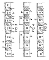
- a photoresist layer 40 is deposited and developed.
- the exposed portions of silicon dioxide layer 14 beneath the openings in photoresist layer 40 are vertically etched to the surface of substrate 10 by RIE to form openings 41, 42, and 43.
- boron is implanted to a dose of approximately 2 x 10¹³ to 2 x 10¹⁴ atoms/cm2 at an energy of approximately 120 KeV and photoresist layer 40 is removed.
- the implant in openings 41 and 42 is used to form a guard ring around the bipolar device.
- the bipolar device is separated from the guard ring by oxide walls 44 and 45.
- the implant in opening 43 is used to ensure a continuous P-well for an NMOS structure after the process is complete.
- the PMOS device is isolated from the NMOS device by an oxide wall 50, thus providing full dielectric isolation between opposite type MOS transistors.
- An added benefit of the boron implant is the lowering of substrate resistance R S which is beneficial in latch-up suppression.
- the P and N regions are separately formed, only two masking steps have been required. This eliminates one masking step from conventional techniques wherein a mask is required for active region definition and for each implant. Additionally, the process according to the present invention avoids the necessity of dealing with a photoresist mask in peaks and valleys of the active regions.
- the minimum distance between two adjacent NMOS devices is 0.5 microns or the resolution of the patterning tool.
- the distance between two adjacent PMOS devices is also 0.5 microns, since they can share the same N-well.
- wall 45 preferably is wider by 0.4 to 0.6 microns than wall 30 to ensure isolation of the PMOS or the second bipolar device from the adjacent bipolar device.
- the minimum width for oxide wall 50, which forms the isolation region between the NMOS and PMOS devices is the larger of a) the minimum resolution of the patterning tool plus one registration tolerance, or b) two registration tolerances.
- the bipolar collector-substrate capacitance is substantially reduced.
- the adjustment of this capacitance is by boron and phosphorous implant doses, the width of oxide wall 44, and total heat treatment included in the process.
- this capacitance can be the absolute minimum.
- some designs may not require an NPN bipolar device next to an NMOS device, thus ensuring a low collector-to-substrate capacitance.
- undoped epitaxial silicon is selectively grown to the thickness of the remaining portions of silicon dioxide layer 14, 24, 26, 41, 42, and 43. This may be accomplished by a five minute in situ hydrogen bake at 1000°C and 25 torr, followed by SEG deposition at 850° - 950°C and 25 torr in a hydrogen dichlorosilane and hydrogen chloride ambient to minimize faceting. This forms a collector region 51 in opening 22, a base/emitter region 52 in opening 24, a guard ring region 53 in opening 41 and 42, a PMOS region 54 in opening 26, and an NMOS region 55 in opening 43.
- guard ring region 53 is shown as separate regions in cross section, it is actually a continuous region encircling collector region 51 and base/emitter region 52. Thereafter, a thin silicon dioxide layer 48 is grown to a thickness of approximately 200-300 angstroms to alleviate the stress at the epi-isolation oxide interface. Oxide layer 48 also is used as a sacrificial oxide for gate oxide integrity improvement.
- a photoresist layer (not shown) is deposited and developed for exposing collector region 51, base/emitter region 52, and PMOS region 54.
- the exposed regions then are implanted with phosphorous to a concentration of approximately 1 x 10¹² to 4 x 10¹² atoms/cm2 at an energy of 150 KeV for setting the N-well impurity profile at the surfaces of the P-channel devices and bipolar devices if necessary.
- the photoresist layer is removed, and a new photoresist layer 56 is deposited and developed to expose guard ring region 53 and NMOS region 55.
- the exposed regions then are implanted with boron for setting the impurity profile for the bipolar guard ring and the P-well for the N-channel devices.
- photoresist layer 56 may not be necessary, and a blanket V T implant may be all that is required to set the correct P-channel and N-channel threshold voltages and to dope the bipolar guard rings.
- substrate 10 is placed in an inert environment at 1050°C for approximately 60 minutes so that the substrate buried layers join with their respective N-well and P-well surface implants.
- a V T implant is performed with BF2 to a concentration of 1 x 10¹² to 3 x 10¹² atoms/cm2.
- the thin sacrificial oxide layer 48 then is removed, and a gate oxide layer 60 having a thickness of 120-150 angstroms is grown, as shown in Fig. 5.
- This thin oxidation is the only oxidation step that the impurities will see, and thus segregation and depletion of boron on the sidewalls of isolation regions are minimized. No birds-beak encroachment is encountered in this process; thus, defined active and isolation dimensions will be the true electrical dimensions of the device and can be 0.5 micron or even less.
- the gate material can be polysilicon, silicide, or a combination of the two.
- P+ polysilicon for P-channels and N+ polysilicon for N-channels are desirable. This is accomplished by doping the polysilicon at the time of the source/drain implants.
- the two types of polysilicon can be shorted by a silicide or a metal strap.
- contacts to the N-well and substrate can be implemented, although they are not shown in these figures. These contacts are presumed to be in planes perpendicular to the plane of the cross sections. Sidewall spacers on gates are formed, and source-drain-gate silicidation is performed. Posts or unguarded contacts can be used for minimizing the interconnect real estate.
- a guard ring should he formed for each bipolar transistor, but the precision of the present process allows the guard ring to be accurately spaced to provide very high performance.
- the base is implanted, and base/emitter contacts (e.g., polysilicon buried contacts) are formed.
- base/emitter contacts e.g., polysilicon buried contacts
- gate oxide layer 60 is grown, and before the N-well mask and implant, a collector sink mask, phosphorous implant (in collector region 5) to a concentration of 1 x 10¹⁵ to 1 x 10¹⁶ atoms/cm2, and a drive-in may be performed for performance improvement.
Landscapes
- Metal-Oxide And Bipolar Metal-Oxide Semiconductor Integrated Circuits (AREA)
- Bipolar Transistors (AREA)
Applications Claiming Priority (2)
| Application Number | Priority Date | Filing Date | Title |
|---|---|---|---|
| US07/320,011 US5010034A (en) | 1989-03-07 | 1989-03-07 | CMOS and bipolar fabrication process using selective epitaxial growth scalable to below 0.5 micron |
| US320011 | 1989-03-07 |
Publications (1)
| Publication Number | Publication Date |
|---|---|
| EP0386574A1 true EP0386574A1 (de) | 1990-09-12 |
Family
ID=23244490
Family Applications (1)
| Application Number | Title | Priority Date | Filing Date |
|---|---|---|---|
| EP90103678A Withdrawn EP0386574A1 (de) | 1989-03-07 | 1990-02-26 | CMOS- und Bipolar-Herstellungsverfahren durch selektives, epitaxiales Aufwachsen zur Dimensionierung unterhalb von 0,5 Mikron |
Country Status (3)
| Country | Link |
|---|---|
| US (1) | US5010034A (de) |
| EP (1) | EP0386574A1 (de) |
| JP (1) | JPH02278761A (de) |
Cited By (1)
| Publication number | Priority date | Publication date | Assignee | Title |
|---|---|---|---|---|
| EP0933801A1 (de) * | 1998-01-30 | 1999-08-04 | STMicroelectronics S.A. | Verfahren zur Abscheidung eines Gebietes aus monokristallinem Silizium |
Families Citing this family (9)
| Publication number | Priority date | Publication date | Assignee | Title |
|---|---|---|---|---|
| JPH0671073B2 (ja) * | 1989-08-29 | 1994-09-07 | 株式会社東芝 | 半導体装置及びその製造方法 |
| US5554562A (en) * | 1995-04-06 | 1996-09-10 | Advanced Micro Devices, Inc. | Advanced isolation scheme for deep submicron technology |
| US5795809A (en) * | 1995-05-25 | 1998-08-18 | Advanced Micro Devices, Inc. | Semiconductor wafer fabrication process including gettering utilizing a combined oxidation technique |
| US6143073A (en) * | 1998-11-19 | 2000-11-07 | Heraeus Shin-Etsu America | Methods and apparatus for minimizing white point defects in quartz glass crucibles |
| KR100275962B1 (ko) | 1998-12-30 | 2001-02-01 | 김영환 | 반도체장치 및 그의 제조방법_ |
| KR100355034B1 (ko) * | 1999-07-15 | 2002-10-05 | 삼성전자 주식회사 | 선택적 에피택셜 성장층을 가진 반도체 장치 및 그 소자분리방법 |
| FR2855650B1 (fr) * | 2003-05-30 | 2006-03-03 | Soitec Silicon On Insulator | Substrats pour systemes contraints et procede de croissance cristalline sur un tel substrat |
| US20050104156A1 (en) * | 2003-11-13 | 2005-05-19 | Texas Instruments Incorporated | Forming a semiconductor structure in manufacturing a semiconductor device using one or more epitaxial growth processes |
| CN102751229B (zh) | 2011-04-20 | 2015-09-30 | 中国科学院微电子研究所 | 浅沟槽隔离结构、其制作方法及基于该结构的器件 |
Citations (4)
| Publication number | Priority date | Publication date | Assignee | Title |
|---|---|---|---|---|
| US4101350A (en) * | 1975-03-06 | 1978-07-18 | Texas Instruments Incorporated | Self-aligned epitaxial method for the fabrication of semiconductor devices |
| EP0134504A1 (de) * | 1983-07-15 | 1985-03-20 | Kabushiki Kaisha Toshiba | CMOS-Vorrichtung und Verfahren zu ihrer Herstellung |
| US4547231A (en) * | 1983-07-08 | 1985-10-15 | Mitsubishi Denki Kabushiki Kaisha | Method of manufacturing semiconductor device utilizing selective epitaxial growth under reduced pressure |
| FR2631741A1 (fr) * | 1988-05-20 | 1989-11-24 | Samsung Electronics Co Ltd | Formation de murs d'isolation entre les regions actives d'un circuit integre |
Family Cites Families (11)
| Publication number | Priority date | Publication date | Assignee | Title |
|---|---|---|---|---|
| US3305913A (en) * | 1964-09-11 | 1967-02-28 | Northern Electric Co | Method for making a semiconductor device by diffusing impurities through spaced-apart holes in a non-conducting coating to form an overlapped diffused region by means oftransverse diffusion underneath the coating |
| FR1569872A (de) * | 1968-04-10 | 1969-06-06 | ||
| DE1811136A1 (de) * | 1968-11-27 | 1970-11-05 | Telefunken Patent | Verfahren zum Herstellen eines Planartransistors |
| DE2007627B2 (de) * | 1970-02-19 | 1973-03-22 | Licentia Patent-Verwaltungs-Gmbh, 6000 Frankfurt | Verfahren zum herstellen einer integrierten halbleiterschaltung |
| US4099998A (en) * | 1975-11-03 | 1978-07-11 | General Electric Company | Method of making zener diodes with selectively variable breakdown voltages |
| US4004954A (en) * | 1976-02-25 | 1977-01-25 | Rca Corporation | Method of selective growth of microcrystalline silicon |
| US4177095A (en) * | 1977-02-25 | 1979-12-04 | National Semiconductor Corporation | Process for fabricating an integrated circuit subsurface zener diode utilizing conventional processing steps |
| JPS5848968A (ja) * | 1981-09-18 | 1983-03-23 | Fujitsu Ltd | 半導体装置の製造方法 |
| JPS58131748A (ja) * | 1982-01-29 | 1983-08-05 | Fujitsu Ltd | 半導体装置の製造方法 |
| US4551909A (en) * | 1984-03-29 | 1985-11-12 | Gte Laboratories Incorporated | Method of fabricating junction field effect transistors |
| JPS62204576A (ja) * | 1986-03-04 | 1987-09-09 | Nec Corp | 縦型トランジスタの製造方法 |
-
1989
- 1989-03-07 US US07/320,011 patent/US5010034A/en not_active Expired - Lifetime
-
1990
- 1990-02-26 EP EP90103678A patent/EP0386574A1/de not_active Withdrawn
- 1990-03-07 JP JP2053869A patent/JPH02278761A/ja active Pending
Patent Citations (4)
| Publication number | Priority date | Publication date | Assignee | Title |
|---|---|---|---|---|
| US4101350A (en) * | 1975-03-06 | 1978-07-18 | Texas Instruments Incorporated | Self-aligned epitaxial method for the fabrication of semiconductor devices |
| US4547231A (en) * | 1983-07-08 | 1985-10-15 | Mitsubishi Denki Kabushiki Kaisha | Method of manufacturing semiconductor device utilizing selective epitaxial growth under reduced pressure |
| EP0134504A1 (de) * | 1983-07-15 | 1985-03-20 | Kabushiki Kaisha Toshiba | CMOS-Vorrichtung und Verfahren zu ihrer Herstellung |
| FR2631741A1 (fr) * | 1988-05-20 | 1989-11-24 | Samsung Electronics Co Ltd | Formation de murs d'isolation entre les regions actives d'un circuit integre |
Non-Patent Citations (5)
| Title |
|---|
| Extended Abstracts, Vol. 87-1, No. 1, Spring 1987, page 215, Philadelphia, PA, US; N. ENDO et al.: "Selective epitaxial technology for scaled CMOS", whole document. * |
| IBM Technical Disclosure Bulletin, Vol. 22, No. 7, December 1979, pages 2946,2947, New York, US; W.P. DUMKE: "Bipolar isolation technique", whole document. * |
| IEEE Transactions on Electron Devices, Vol. ED-33, No. 11, November 1986, pages 1738-1744, New York, US; S. NAGAO et al.: "Application of Selective Silicon Epitaxial Growth for CMOS Technology", page 1739; figure 2. * |
| International Electron Devices Meeting, Technical Digest, 5-7th December 1983, pages 31-34, New York, US; N. ENDO et al.: "CMOS technology using SEG isolation technique", page 32, left column; figures 3,4b. * |
| International Electron Devices Meeting, Technical Digest, 6-9th December 1987, pages 20-23, New York, US; J. MANOLIU et al.: "A submicron dual buried layer twin well CMOS SEG process", page 20, process description; figure 1. * |
Cited By (2)
| Publication number | Priority date | Publication date | Assignee | Title |
|---|---|---|---|---|
| EP0933801A1 (de) * | 1998-01-30 | 1999-08-04 | STMicroelectronics S.A. | Verfahren zur Abscheidung eines Gebietes aus monokristallinem Silizium |
| FR2774509A1 (fr) * | 1998-01-30 | 1999-08-06 | Sgs Thomson Microelectronics | Procede de depot d'une region de silicium monocristallin |
Also Published As
| Publication number | Publication date |
|---|---|
| JPH02278761A (ja) | 1990-11-15 |
| US5010034A (en) | 1991-04-23 |
Similar Documents
| Publication | Publication Date | Title |
|---|---|---|
| US5424572A (en) | Spacer formation in a semiconductor structure | |
| US5169794A (en) | Method of fabrication of pnp structure in a common substrate containing npn or MOS structures | |
| US5455189A (en) | Method of forming BICMOS structures | |
| EP0375585B1 (de) | Verfahren zum Herstellen einer BICMOS-Anordnung | |
| CA1267444A (en) | Bicmos process having narrow bipolar emitter and implanted aluminum isolation | |
| EP1030363B1 (de) | Integration bipolarer und CMOS Bauelemente für 0.1 Mikrometer Transistoren | |
| JPH04226066A (ja) | Bicmos装置及びその製造方法 | |
| US5082796A (en) | Use of polysilicon layer for local interconnect in a CMOS or BiCMOS technology incorporating sidewall spacers | |
| EP0450375B1 (de) | Kontaktierung und deren Herstellungsverfahren für Halbleiterbauelemente | |
| KR100196483B1 (ko) | 고 성능 bicmos 회로를 제조하는 방법 | |
| US6943413B2 (en) | BI-CMOS integrated circuit | |
| US5010034A (en) | CMOS and bipolar fabrication process using selective epitaxial growth scalable to below 0.5 micron | |
| US5443994A (en) | Method of fabricating a semiconductor device having a borosilicate glass spacer | |
| US5422290A (en) | Method of fabricating BiCMOS structures | |
| US5081518A (en) | Use of a polysilicon layer for local interconnect in a CMOS or BICMOS technology incorporating sidewall spacers | |
| KR100227872B1 (ko) | 반도체장치 및 그 제조 방법 | |
| US6011283A (en) | Pillar emitter for BiCMOS devices | |
| US5227654A (en) | Semiconductor device with improved collector structure | |
| US6080612A (en) | Method of forming an ultra-thin SOI electrostatic discharge protection device | |
| US5970347A (en) | High performance mosfet transistor fabrication technique | |
| EP0398247B1 (de) | Halbleitervorrichtung und Verfahren zu seiner Herstellung | |
| EP0961316A2 (de) | Verfahren zur Herstellung eines integrierten, vertikalen Bipolartransistors | |
| JP2889246B2 (ja) | 半導体装置 | |
| JPH1065033A (ja) | BiCMOS集積回路およびその製造方法 | |
| EP0849791A1 (de) | Verbesserungen an oder in Bezug auf Halbleiteranordnungen |
Legal Events
| Date | Code | Title | Description |
|---|---|---|---|
| PUAI | Public reference made under article 153(3) epc to a published international application that has entered the european phase |
Free format text: ORIGINAL CODE: 0009012 |
|
| AK | Designated contracting states |
Kind code of ref document: A1 Designated state(s): DE FR GB IT NL |
|
| 17P | Request for examination filed |
Effective date: 19910117 |
|
| 17Q | First examination report despatched |
Effective date: 19930614 |
|
| STAA | Information on the status of an ep patent application or granted ep patent |
Free format text: STATUS: THE APPLICATION IS DEEMED TO BE WITHDRAWN |
|
| 18D | Application deemed to be withdrawn |
Effective date: 19961120 |