EP0388891A2 - Dispositif semi-conducteur - Google Patents
Dispositif semi-conducteur Download PDFInfo
- Publication number
- EP0388891A2 EP0388891A2 EP90105245A EP90105245A EP0388891A2 EP 0388891 A2 EP0388891 A2 EP 0388891A2 EP 90105245 A EP90105245 A EP 90105245A EP 90105245 A EP90105245 A EP 90105245A EP 0388891 A2 EP0388891 A2 EP 0388891A2
- Authority
- EP
- European Patent Office
- Prior art keywords
- semiconductor device
- wiring
- wiring pattern
- semiconductor
- insulating layer
- Prior art date
- Legal status (The legal status is an assumption and is not a legal conclusion. Google has not performed a legal analysis and makes no representation as to the accuracy of the status listed.)
- Granted
Links
Images


Classifications
-
- H—ELECTRICITY
- H10—SEMICONDUCTOR DEVICES; ELECTRIC SOLID-STATE DEVICES NOT OTHERWISE PROVIDED FOR
- H10B—ELECTRONIC MEMORY DEVICES
- H10B20/00—Read-only memory [ROM] devices
-
- H—ELECTRICITY
- H10—SEMICONDUCTOR DEVICES; ELECTRIC SOLID-STATE DEVICES NOT OTHERWISE PROVIDED FOR
- H10B—ELECTRONIC MEMORY DEVICES
- H10B20/00—Read-only memory [ROM] devices
- H10B20/27—ROM only
- H10B20/30—ROM only having the source region and the drain region on the same level, e.g. lateral transistors
- H10B20/34—Source electrode or drain electrode programmed
-
- H—ELECTRICITY
- H10—SEMICONDUCTOR DEVICES; ELECTRIC SOLID-STATE DEVICES NOT OTHERWISE PROVIDED FOR
- H10W—GENERIC PACKAGES, INTERCONNECTIONS, CONNECTORS OR OTHER CONSTRUCTIONAL DETAILS OF DEVICES COVERED BY CLASS H10
- H10W20/00—Interconnections in chips, wafers or substrates
- H10W20/01—Manufacture or treatment
- H10W20/031—Manufacture or treatment of conductive parts of the interconnections
- H10W20/056—Manufacture or treatment of conductive parts of the interconnections by filling conductive material into holes, grooves or trenches
-
- H—ELECTRICITY
- H10—SEMICONDUCTOR DEVICES; ELECTRIC SOLID-STATE DEVICES NOT OTHERWISE PROVIDED FOR
- H10W—GENERIC PACKAGES, INTERCONNECTIONS, CONNECTORS OR OTHER CONSTRUCTIONAL DETAILS OF DEVICES COVERED BY CLASS H10
- H10W20/00—Interconnections in chips, wafers or substrates
- H10W20/01—Manufacture or treatment
- H10W20/071—Manufacture or treatment of dielectric parts thereof
- H10W20/081—Manufacture or treatment of dielectric parts thereof by forming openings in the dielectric parts
Definitions
- This invention relates to a semiconductor device, and more specifically to a semiconductor device to be customized with a use of wirings.
- a custom product is a semiconductor memory device which is programmed by the manufacturer himself; for example, a mask ROM.
- a typical mask ROM comprises a plurality of memory cells each of which is constituted by, for example, an MOS transistor, each MOS transistor having a gate connected so as to receive a reading voltage, a source connected to a reference potential terminal, and a drain selectively connected to a data output line, in accordance with data "1" or "0" in the programming.
- the data output line is connected to the power source potential terminal via a load circuit.
- the reading voltage is applied to one of the MOS transistors during the reading operation, so that the MOS transistor is in an ON state.
- the data output line is set at a potential equal to that of the reference potential terminal if the drain of the MOS transistor is connected to the data output line, and at a potential equal to that of the power source potential terminal if the drain is open.
- Semiconductor memory devices such as that described above are often incorporated in equipment which is in temporary demand. Consequently, the volume of sales of such equipment may well depend on the speed at which the semiconductor memory device in question can be delivered. Therefore, it is necessary that such a semiconductor memory device be able to be delivered within a much shorter period of time than standard custom products.
- the conventional custom semiconductor memory device requires a relatively large number of manufacturing steps following the reception of an order; i.e., the step of depositing an aluminum layer on the semiconductor structure including memory cells; patterning the aluminum layer to form a wiring pattern including wiring lines for connecting memory cells storing data "1" to the data output line; forming a passivation layer which covers the wiring lines; forming openings in the passivation layer so that part of the wiring pattern can be used as a bonding pad. Because of the number of the steps involved, it is therefore difficult to deliver a conventional semiconductor memory device to the customer within a relatively short period of time.
- the object of the present invention is to provide a semiconductor device which, upon receipt of an order, can be customized in a small number of manufacturing steps.
- a semiconductor device comprising: a semiconductor substrate; semiconductor elements formed in the semiconductor substrate; a wiring pattern formed on the semiconductor substrate, for wiring the semiconductor elements; and an insulating layer covering the wiring pattern, wherein the wiring pattern includes a plurality of connecting sections each selectively set to a conductive state by conductive material filled in an opening formed in the insulating layer.
- the semiconductor device thus arranged is customized by forming the openings in the insulating layer and supplying conductive material into the openings after receipt of an order. Since the wiring pattern and the insulating layer are formed beforehand, it is therefore not necessary to perform the steps of depositing a conductive layer on the substrate, patterning the conductive layer as wiring, and forming an insulating layer which covers the patterned conductive layer. Hence, the semiconductor device of the present invention can be delivered within a short period of time following the receipt of an order therefor.
- Fig. 1 is a schematic diagram showing the circuit structure of the semiconductor memory device
- Fig. 2 is a plan view showing part of the wiring pattern of the semiconductor memory device
- Fig. 3 is a cross sectional view showing the semiconductor memory device taken along the line I-I in Fig. 2.
- the semiconductor memory device of the present invention has a plurality of n-channel MOS transistors MC arranged in a matrix fashion and each serving as a memory cell, a plurality of word lines WL extending in row directions, and a plurality of bit lines BL extending in column directions.
- the semiconductor memory device is in a programmed state.
- the MOS transistors MC connected to the word line WL are turned on.
- the potential of each bit line BL depends on whether or not the drain of a corresponding MOS transistor MC is connected to the bit line BL. If the MOS transistor MC is connected to the bit line BL, the potential of the bit line BL is set at the ground level, whereas if the MOS transistor MC is not connected to the bit line BL, the potential thereof is set at the power source level.
- the source and drain of the MOS transistor MC are constituted by n-type semiconductor regions 11 and 12 formed in the surface region of p-type semiconductor substrate 10, respectively.
- the gate of the MOS transistor MC is constituted by a gate electrode layer 13 formed on and insulated from that portion of substrate 10 which is located between semiconductor regions 11 and 12.
- the semiconductor memory device has an aluminum wiring pattern PT formed on SiO2 insulating layer 14 covering the semiconductor regions 11 and 12 and the gate electrode 13.
- the wiring pattern PT includes lines serving as source electrode SL, word line WL, drain electrode DL, and bit lines BL, as shown in Fig. 2.
- the source electrodes SL, the word lines WL, and the drain electrodes DL are respectively connected to the semiconductor region 11, the gate electrode 13, and the semiconductor region 12 via contact holes formed in the insulating layer 14.
- Each of the lines in the Al wiring pattern PT is 0.8 ⁇ m thick, in 0.7 ⁇ m width, with the interval between the lines also being 0.7 ⁇ m. Similarly, the interval between the drain electrode DL and the bit line BL is 0.7 ⁇ m.
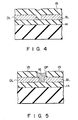
- a passivation layer 15 is accumulated on the Al wiring pattern PT by means of an ordinary CVD method or a vacuum CVD method, so as to have a thickness of 1.2 ⁇ m.
- the passivation layer 15 has a double-layer structure including, for example, a PSG layer and a plasma SiN layer.
- the passivation layer 15 is etched by isotropic etching or anisotropic etching, so that openings OP are formed over the memory cells selected by the customer order.
- the size of the openings OP is set larger than 0.7 ⁇ m, i.e. the interval between the drain electrode DL and the bit line BL; for example, at 1 ⁇ m ⁇ 1 ⁇ m. For this reason, the end portions of the drain electrode DL and the bit line BL are exposed via the opening OP.
- a mask alignment error may often occur.
- the size of the opening OP is set sufficiently large in consideration of such error, to ensure that the end portions of the drain electrode DL and the bit line BL are exposed.
- a contact layer 16 is formed in the opening OP to connect the drain electrode DL and the bit line BL.
- the contact layer 16 is formed by means of a selective CVD method utilizing the reaction between WF and H or WF and SiH, in which W is selectively deposited to the exposed portion of the drain electrode DL and the bit line BL. In this step, W is deposited at the same rate both on the end surface of the drain electrode DL and the end surface of the bit line BL. This causes a W layer to grow in a direction from the inner surface of the opening OP toward the center thereof.
- the W layer is formed 0.6 ⁇ m thick.
- metal material such as Ni may be selectively deposited on the Al layer by means of electroless plating.
- the metal material is not accumulated on passivation layer 15. Hence, a reliable contact can be obtained between the drain electrode DL and the bit line BL.
- the opening OP may be formed in the same manufacturing step as that for forming opening OP2 for exposing bonding pad PD covered by the passivation layer 15. Therefore, an additional manufacturing step is not required to form the opening OP.
- an opening OP is formed to expose portions of the drain electrode DL and the bit line BL.
- an opening may be formed to expose portions of any two wiring lines which are selectively connected to each other, upon receipt of customer,s order.
- the distance between the exposed portions of the wiring lines it is set as shorter as possible since the deposition of the conductive material must be continued until the wiring lines are connected to each other.
- the distance is set less than the thickness of the passivation layer, the contact layer formed by the deposition can be prevented from spreading out from the opening OP.
- the opening is set small in accordance with the distance between the wiring lines, it is possible to connecting the wiring layer without forming any gap within the contact layer, which may increase the contact resistance between the wiring lines. Therefore, the distance between the wiring lines and the size of the opening OP must be determined according to a design rule for the wiring lines.
- a semiconductor memory device is manufactured in a full-custom manner.
- the present invention can be applied to a semiconductor memory device manufactured in a semi-custom manner, which uses a gate array, a sea of gates, or the like.
- Fig.8 shows an example in which a gate array is used.
- the semiconductor memory device has a multi-layered structure. That is, the drain electrode DL is constituted by first layer DL1 and second layer DL2, which are connected via contact hole VH formed in interlayer insulating layer 20.
- the wiring pattern includes pairs of wiring lines (i.e., drain electrode DL and bit line BL) which are kept unconnected, the passivation layer is formed to cover this wiring pattern.
- the opening OP is formed to expose portions of the wiring line pair selected according to data "1", for example, and metal material 16 is deposited on and connects the exposed portions of the paired wiring lines.
Landscapes
- Semiconductor Memories (AREA)
- Internal Circuitry In Semiconductor Integrated Circuit Devices (AREA)
- Design And Manufacture Of Integrated Circuits (AREA)
Applications Claiming Priority (3)
| Application Number | Priority Date | Filing Date | Title |
|---|---|---|---|
| JP1068826A JP2647188B2 (ja) | 1989-03-20 | 1989-03-20 | 半導体装置の製造方法 |
| JP68826/89 | 1989-03-20 | ||
| JP6882689 | 1989-03-20 |
Publications (3)
| Publication Number | Publication Date |
|---|---|
| EP0388891A2 true EP0388891A2 (fr) | 1990-09-26 |
| EP0388891A3 EP0388891A3 (fr) | 1991-11-21 |
| EP0388891B1 EP0388891B1 (fr) | 2001-09-12 |
Family
ID=13384901
Family Applications (1)
| Application Number | Title | Priority Date | Filing Date |
|---|---|---|---|
| EP90105245A Expired - Lifetime EP0388891B1 (fr) | 1989-03-20 | 1990-03-20 | Dispositif semi-conducteur |
Country Status (5)
| Country | Link |
|---|---|
| US (1) | US5164814A (fr) |
| EP (1) | EP0388891B1 (fr) |
| JP (1) | JP2647188B2 (fr) |
| KR (1) | KR930009018B1 (fr) |
| DE (1) | DE69033794T2 (fr) |
Cited By (2)
| Publication number | Priority date | Publication date | Assignee | Title |
|---|---|---|---|---|
| EP0666599A3 (fr) * | 1994-02-04 | 1998-07-01 | Advanced Micro Devices, Inc. | Matrice de transistors programmée par métal |
| WO2001091185A3 (fr) * | 2000-05-19 | 2002-03-28 | Motorola Inc | Memoire rom a programmation ultra tardive et procede de fabrication |
Families Citing this family (9)
| Publication number | Priority date | Publication date | Assignee | Title |
|---|---|---|---|---|
| JP2911980B2 (ja) * | 1990-08-18 | 1999-06-28 | 日本電気株式会社 | 半導体集積回路装置 |
| JP2681427B2 (ja) * | 1992-01-06 | 1997-11-26 | 三菱電機株式会社 | 半導体装置 |
| US5455461A (en) * | 1992-09-21 | 1995-10-03 | Fujitsu Limited | Semiconductor device having reformed pad |
| US5244299A (en) * | 1992-12-04 | 1993-09-14 | Chu Wei Y | Apparatus used in writing and massaging alternatively |
| JPH06333944A (ja) * | 1993-05-25 | 1994-12-02 | Nippondenso Co Ltd | 半導体装置 |
| US5985717A (en) * | 1996-05-06 | 1999-11-16 | United Microelectronics Corp. | Method of fabricating a semiconductor device |
| US6111756A (en) * | 1998-09-11 | 2000-08-29 | Fujitsu Limited | Universal multichip interconnect systems |
| US6570235B2 (en) * | 2001-03-20 | 2003-05-27 | Macronix International Co., Ltd. | Cells array of mask read only memory |
| US7053447B2 (en) * | 2004-09-14 | 2006-05-30 | Infineon Technologies Ag | Charge-trapping semiconductor memory device |
Family Cites Families (9)
| Publication number | Priority date | Publication date | Assignee | Title |
|---|---|---|---|---|
| JPS59198733A (ja) * | 1983-04-26 | 1984-11-10 | Mitsubishi Electric Corp | 半導体集積回路装置 |
| JPS62260340A (ja) * | 1986-05-06 | 1987-11-12 | Toshiba Corp | 半導体装置の製造方法 |
| JPS62263653A (ja) * | 1986-05-12 | 1987-11-16 | Hitachi Ltd | 半導体集積回路装置の製造方法 |
| JPH084089B2 (ja) * | 1986-12-22 | 1996-01-17 | 株式会社日立製作所 | Ic素子並びにic素子における配線接続方法 |
| JPS6317543A (ja) * | 1986-07-10 | 1988-01-25 | Nec Corp | 配線修正方法 |
| JPS6370440A (ja) * | 1986-09-11 | 1988-03-30 | Mitsubishi Electric Corp | 半導体集積回路装置 |
| JPS6371538U (fr) * | 1986-10-30 | 1988-05-13 | ||
| JPS63278256A (ja) * | 1987-05-09 | 1988-11-15 | Mitsubishi Electric Corp | 半導体装置およびその製造方法 |
| JP2527183B2 (ja) * | 1987-05-20 | 1996-08-21 | 株式会社日立製作所 | 処理方法及び半導体装置の配線修正方法 |
-
1989
- 1989-03-20 JP JP1068826A patent/JP2647188B2/ja not_active Expired - Fee Related
-
1990
- 1990-03-20 DE DE69033794T patent/DE69033794T2/de not_active Expired - Fee Related
- 1990-03-20 KR KR1019900003731A patent/KR930009018B1/ko not_active Expired - Fee Related
- 1990-03-20 EP EP90105245A patent/EP0388891B1/fr not_active Expired - Lifetime
-
1991
- 1991-09-04 US US07/759,818 patent/US5164814A/en not_active Expired - Lifetime
Cited By (3)
| Publication number | Priority date | Publication date | Assignee | Title |
|---|---|---|---|---|
| EP0666599A3 (fr) * | 1994-02-04 | 1998-07-01 | Advanced Micro Devices, Inc. | Matrice de transistors programmée par métal |
| WO2001091185A3 (fr) * | 2000-05-19 | 2002-03-28 | Motorola Inc | Memoire rom a programmation ultra tardive et procede de fabrication |
| US6498066B2 (en) | 2000-05-19 | 2002-12-24 | Motorola, Inc. | Ultra-late programming ROM and method of manufacture |
Also Published As
| Publication number | Publication date |
|---|---|
| JPH02246364A (ja) | 1990-10-02 |
| DE69033794T2 (de) | 2002-05-02 |
| US5164814A (en) | 1992-11-17 |
| EP0388891A3 (fr) | 1991-11-21 |
| KR930009018B1 (ko) | 1993-09-18 |
| EP0388891B1 (fr) | 2001-09-12 |
| KR900015301A (ko) | 1990-10-26 |
| JP2647188B2 (ja) | 1997-08-27 |
| DE69033794D1 (de) | 2001-10-18 |
Similar Documents
| Publication | Publication Date | Title |
|---|---|---|
| US6635918B1 (en) | Semiconductor integrated circuit device and method for manufacturing the same | |
| KR100201182B1 (ko) | 반도체집적회로장치 | |
| US5237187A (en) | Semiconductor memory circuit device and method for fabricating same | |
| US6423992B2 (en) | Semiconductor integrated circuit device | |
| US20020155662A1 (en) | Method of manufacturing a semiconductor integrated circuit device having a memory cell array and a peripheral circuit region | |
| US5521860A (en) | CMOS static memory | |
| JPH0661442A (ja) | プログラマブル・ゲート・アレー及びその製造方法 | |
| EP0388891A2 (fr) | Dispositif semi-conducteur | |
| US5128744A (en) | Semiconductor integrated circuit and method of manufacturing same | |
| US6078074A (en) | Semiconductor device having multilayer metal interconnection | |
| US5358886A (en) | Method of making integrated circuit structure with programmable conductive electrode/interconnect material | |
| EP0482556A1 (fr) | Elément de résistance en polysilicium et dispositif à semi-conducteur l'utilisant | |
| US7601630B2 (en) | Semiconductor device and method for fabricating the same | |
| US6384449B2 (en) | Nonvolatile memory and method for fabricating the same | |
| US5824579A (en) | Method of forming shared contact structure | |
| US5303186A (en) | Semiconductor memory and process for manufacturing the same | |
| US6303422B1 (en) | Semiconductor memory and manufacturing method thereof | |
| US6174764B1 (en) | Process for manufacturing integrated circuit SRAM | |
| US5285110A (en) | Interconnection structure in semiconductor device | |
| JPH0821638B2 (ja) | 不揮発性半導体記憶装置およびその製造方法 | |
| JP3279263B2 (ja) | 不揮発性半導体記憶装置の製造方法 | |
| US20020025611A1 (en) | MasK ROM and method for fabricating the same | |
| JPH10247691A (ja) | 半導体記憶装置 | |
| US6355982B2 (en) | Semiconductor memory device having pairs of bit lines arranged on both sides of memory cells | |
| US5027175A (en) | Integrated circuit semiconductor device having improved wiring structure |
Legal Events
| Date | Code | Title | Description |
|---|---|---|---|
| PUAI | Public reference made under article 153(3) epc to a published international application that has entered the european phase |
Free format text: ORIGINAL CODE: 0009012 |
|
| 17P | Request for examination filed |
Effective date: 19900320 |
|
| AK | Designated contracting states |
Kind code of ref document: A2 Designated state(s): DE FR GB |
|
| PUAL | Search report despatched |
Free format text: ORIGINAL CODE: 0009013 |
|
| AK | Designated contracting states |
Kind code of ref document: A3 Designated state(s): DE FR GB |
|
| 17Q | First examination report despatched |
Effective date: 19930507 |
|
| APAD | Appeal reference recorded |
Free format text: ORIGINAL CODE: EPIDOS REFNE |
|
| APAB | Appeal dossier modified |
Free format text: ORIGINAL CODE: EPIDOS NOAPE |
|
| GRAG | Despatch of communication of intention to grant |
Free format text: ORIGINAL CODE: EPIDOS AGRA |
|
| GRAG | Despatch of communication of intention to grant |
Free format text: ORIGINAL CODE: EPIDOS AGRA |
|
| GRAH | Despatch of communication of intention to grant a patent |
Free format text: ORIGINAL CODE: EPIDOS IGRA |
|
| GRAH | Despatch of communication of intention to grant a patent |
Free format text: ORIGINAL CODE: EPIDOS IGRA |
|
| GRAA | (expected) grant |
Free format text: ORIGINAL CODE: 0009210 |
|
| AK | Designated contracting states |
Kind code of ref document: B1 Designated state(s): DE FR GB |
|
| REF | Corresponds to: |
Ref document number: 69033794 Country of ref document: DE Date of ref document: 20011018 |
|
| REG | Reference to a national code |
Ref country code: GB Ref legal event code: IF02 |
|
| ET | Fr: translation filed | ||
| PLBE | No opposition filed within time limit |
Free format text: ORIGINAL CODE: 0009261 |
|
| STAA | Information on the status of an ep patent application or granted ep patent |
Free format text: STATUS: NO OPPOSITION FILED WITHIN TIME LIMIT |
|
| 26N | No opposition filed | ||
| APAH | Appeal reference modified |
Free format text: ORIGINAL CODE: EPIDOSCREFNO |
|
| PGFP | Annual fee paid to national office [announced via postgrant information from national office to epo] |
Ref country code: FR Payment date: 20060308 Year of fee payment: 17 |
|
| PGFP | Annual fee paid to national office [announced via postgrant information from national office to epo] |
Ref country code: GB Payment date: 20060315 Year of fee payment: 17 |
|
| PGFP | Annual fee paid to national office [announced via postgrant information from national office to epo] |
Ref country code: DE Payment date: 20060316 Year of fee payment: 17 |
|
| GBPC | Gb: european patent ceased through non-payment of renewal fee |
Effective date: 20070320 |
|
| REG | Reference to a national code |
Ref country code: FR Ref legal event code: ST Effective date: 20071130 |
|
| PG25 | Lapsed in a contracting state [announced via postgrant information from national office to epo] |
Ref country code: DE Free format text: LAPSE BECAUSE OF NON-PAYMENT OF DUE FEES Effective date: 20071002 |
|
| PG25 | Lapsed in a contracting state [announced via postgrant information from national office to epo] |
Ref country code: GB Free format text: LAPSE BECAUSE OF NON-PAYMENT OF DUE FEES Effective date: 20070320 |
|
| PG25 | Lapsed in a contracting state [announced via postgrant information from national office to epo] |
Ref country code: FR Free format text: LAPSE BECAUSE OF NON-PAYMENT OF DUE FEES Effective date: 20070402 |